PD - 94083A
IRG4BC15UD-S
IRG4BC15UD-L
INSULATED GATE BIPOLAR TRANSISTOR WITH
ULTRAFAST SOFT RECOVERY DIODE
UltraFast CoPack IGBT
C
Features
• UltraFast: Optimized for high frequencies from10 to
30 kHz in hard switching
• IGBT Co-packaged with ultra-soft-recovery
antiparallel diode
• Industry standard D2Pak & TO-262 packages
VCES = 600V
VCE(on) typ. = 2.02V
G
@VGE = 15V, IC = 7.8A
E
n-ch an nel
Benefits
• Best Value for Appliance and Industrial Applications
• High noise immune "Positive Only" gate driveNegative bias gate drive not necessary
• For Low EMI designs- requires little or no snubbing
• Single Package switch for bridge circuit applications
• Compatible with high voltage Gate Driver IC's
• Allows simpler gate drive
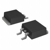
D2Pak
IRG4BC15UD-S
TO-262
IRG4BC15UD-L
Absolute Maximum Ratings
Parameter
VCES
IC @ TC = 25°C
IC @ TC = 100°C
ICM
ILM
IF @ TC = 100°C
IFM
VGE
PD @ TC = 25°C
PD @ TC = 100°C
TJ
TSTG
Collector-to-Emitter Voltage
Continuous Collector Current
Continuous Collector Current
Pulsed Collector Current�Q
Clamped Inductive Load Current R
Diode Continuous Forward Current
Diode Maximum Forward Current
Gate-to-Emitter Voltage
Maximum Power Dissipation
Maximum Power Dissipation
Operating Junction and
Storage Temperature Range
Soldering Temperature, for 10 sec.
Max.
Units
600
14
7.8
42
42
4.0
16
± 20
49
19
-55 to +150
V
A
V
W
°C
300 (0.063 in. (1.6mm) from case)
Thermal Resistance
Parameter
RθJC
RθJC
RθCS
RθJA
RθJA
Wt
www.irf.com
Junction-to-Case - IGBT
Junction-to-Case - Diode
Case-to-Sink, flat, greased surface
Junction-to-Ambient, typical socket mount U
Junction-to-Ambient (PCB Mount, steady state)V
Weight
Min.
Typ.
Max.
–––
–––
–––
–––
–––
–––
–––
–––
0.50
–––
–––
2 (0.07)
2.7
7.0
–––
80
40
–––
Units
°C/W
g (oz)
1
06/12/01
�IRG4BC15UD-S/L
Electrical Characteristics @ TJ = 25°C (unless otherwise specified)
Parameter
Collector-to-Emitter Breakdown VoltageS
∆V(BR)CES/∆TJ Temperature Coeff. of Breakdown Voltage
VCE(on)
Collector-to-Emitter Saturation Voltage
V(BR)CES
VGE(th)
∆VGE(th)/∆TJ
gfe
ICES
VFM
IGES
Min.
600
–––
–––
–––
–––
Gate Threshold Voltage
3.0
Temperature Coeff. of Threshold Voltage –––
Forward Transconductance�T
4.1
Zero Gate Voltage Collector Current
–––
–––
Diode Forward Voltage Drop
–––
–––
Gate-to-Emitter Leakage Current
–––
Typ.
–––
0.63
2.02
2.56
2.21
–––
-10
6.2
–––
–––
1.5
1.4
–––
Max. Units
Conditions
–––
V
VGE = 0V, IC = 250µA
––– V/°C VGE = 0V, IC = 1.0mA
2.4
IC = 7.8A
VGE = 15V
–––
V
IC = 14A
–––
IC = 7.8A, TJ = 150°C
6.0
VCE = VGE, IC = 250µA
––– mV/°C VCE = VGE, IC = 250µA
–––
S
VCE = 100V, IC = 7.8A
250
µA
VGE = 0V, VCE = 600V
1400
VGE = 0V, VCE = 600V, TJ = 150°C
1.8
V
IC = 4.0A
1.7
IC = 4.0A, TJ = 150°C
±100 nA
VGE = ±20V
Switching Characteristics @ TJ = 25°C (unless otherwise specified)
Qg
Qge
Qgc
td(on)
tr
td(off)
tf
Eon
Eoff
Ets
td(on)
tr
td(off)
tf
Ets
LE
Cies
Coes
Cres
trr
Parameter
Total Gate Charge (turn-on)
Gate - Emitter Charge (turn-on)
Gate - Collector Charge (turn-on)
Turn-On Delay Time
Rise Time
Turn-Off Delay Time
Fall Time
Turn-On Switching Loss
Turn-Off Switching Loss
Total Switching Loss
Turn-On Delay Time
Rise Time
Turn-Off Delay Time
Fall Time
Total Switching Loss
Internal Emitter Inductance
Input Capacitance
Output Capacitance
Reverse Transfer Capacitance
Diode Reverse Recovery Time
Irr
Diode Peak Reverse Recovery Current
Qrr
Diode Reverse Recovery Charge
di(rec)M/dt
Diode Peak Rate of Fall of Recovery
During tb
Min.
–––
–––
–––
–––
–––
–––
–––
–––
–––
–––
–––
–––
–––
–––
–––
–––
–––
–––
–––
–––
–––
–––
–––
–––
–––
–––
–––
Typ.
23
4.0
9.6
17
20
160
83
0.24
0.26
0.50
16
21
180
220
0.76
7.5
410
37
5.3
28
38
2.9
3.7
40
70
280
240
Max. Units
Conditions
35
IC = 7.8A
6.0
nC
VCC = 400V
14
VGE = 15V
–––
TJ = 25°C
–––
ns
IC = 7.8A, VCC = 480V
240
VGE = 15V, R G = 75Ω
120
Energy losses include "tail" and
–––
diode reverse recovery.
–––
mJ
0.63
–––
TJ = 150°C,
–––
ns
IC = 7.8A, VCC = 480V
–––
VGE = 15V, R G = 75Ω
–––
Energy losses include "tail" and
–––
mJ diode reverse recovery.
–––
nH
Measured 5mm from package
–––
VGE = 0V
–––
pF
VCC = 30V
–––
ƒ = 1.0MHz
42
ns
TJ = 25°C
57
TJ = 125°C
IF = 4.0A
5.2
A
TJ = 25°C
6.7
TJ = 125°C
VR = 200V
60
nC
TJ = 25°C
110
TJ = 125°C
di/dt 200A/µs
––– A/µs TJ = 25°C
–––
TJ = 125°C
�IRG4BC15UD-S/L
12.00
Duty cycle : 50%
Tj = 125°C
Tsink = 90°C Ta = 55°C
Gate drive as specified
Turn-on losses include effects of
reverse recovery
Power Dissipation = 11W for Heatsink Mount
Power Dissipation = 1.8W for typical
PCB socket Mount
Load Current ( A )
10.00
8.00
60% of rated
voltage
6.00
Ideal diodes
4.00
2.00
0.00
0.1
1
10
100
f , Frequency ( kHz )
Fig. 1 - Typical Load Current vs. Frequency
(Load Current = IRMS of fundamental)
I C , Collector-to-Emitter Current (A)
10
TJ = 150 °C
�
1
TJ = 25 °C
�
V
= 15V
�
20µs PULSE WIDTH
GE
0.1
0.1
1
VCE , Collector-to-Emitter Voltage (V)
Fig. 2 - Typical Output Characteristics
10
I C , Collector-to-Emitter Current (A)
100
100
TJ = 150 °C
�
10
1
TJ = 25 °C
�
V
= 50V
�
5µs PULSE WIDTH
CC
0.1
5.0
10.0
15.0
20.0
VGE , Gate-to-Emitter Voltage (V)
Fig. 3 - Typical Transfer Characteristics
�IRG4BC15UD-S/L
14
VCE , Collector-to Emitter Voltage (V)
4.0
Maximum DC Collector Current(A)
12
10
8
6
4
2
VGE = 15V
80µs PULSE WIDTH
IC = 14A
3.0
IC = 7.8A
2.0
IC = 3.9A
1.0
0
25
50
75
100
125
150
-60 -40 -20
TC , Case Temperature ( °C)
0
20
40
60
80 100 120 140
T J , Junction Temperature (°C)
Fig. 4 - Maximum Collector Current vs. Case
Temperature
Fig. 5 - Typical Collector-to-Emitter Voltage
vs. Junction Temperature
Thermal Response (Z thJC )
10
D = 0.50
1
0.20
�
0.10
0.05
0.1
0.01
0.00001
0.02
0.01
P DM
t1
�
SINGLE PULSE
(THERMAL RESPONSE)
t2
�
Notes:
1. Duty factor D = t 1 / t 2
2. Peak TJ = PDM x Z thJC + TC
0.0001
0.001
0.01
0.1
t1 , Rectangular Pulse Duration (sec)
Fig. 6 - Maximum Effective Transient Thermal Impedance, Junction-to-Case
1
�IRG4BC15UD-S/L
�
20
VGE = 0V,
f = 1MHz
Cies = Cge + Cgc , Cce SHORTED
Cres = Cgc
Coes = Cce + Cgc
600
VGE, Gate-to-Emitter Voltage (V)
C, Capacitance (pF)
800
C ies
�
400
C�
oes
200
C res
�
VCC = 400V
I C = 7.8A
16
12
8
4
0
0
1
10
0
100
5
10
15
20
25
QG , Total Gate Charge (nC)
VCE , Collector-to-Emitter Voltage (V)
Fig. 7 - Typical Capacitance vs.
Collector-to-Emitter Voltage
Fig. 8 - Typical Gate Charge vs.
Gate-to-Emitter Voltage
0.48
10
VCC = 480V
VGE = 15V
TJ = 25°C
I C = 7.8A
Total Switching Losses (mJ)
Total Switching Losses (mJ)
�
0.46
0.44
0.42
RG = 75Ω
VGE = 15V
VCC = 480V
IC = 14A
1
IC = 7.8A
IC = 3.9A
0.1
0
10
20
30
40
R G, Gate Resistance ( Ω )
Fig. 9 - Typical Switching Losses vs. Gate
Resistance
50
-60 -40 -20
0
20
40
60
80 100 120 140 160
T J, Junction Temperature (°C)
Fig. 10 - Typical Switching Losses vs.
Junction Temperature
�IRG4BC15UD-S/L
100
VGE = 20V
TJ = 125°
RG = 75Ω
TJ = 150°C
VGE = 15V
1.6
VCC = 480V
C, Capacitance(pF)
Total Switching Losses (mJ)
2.0
1.2
0.8
SAFE OPERATING AREA
10
0.4
0.0
1
2
4
6
8
10
12
14
16
1
10
IC , Collector Current (A)
100
VDS , Drain-to-Source Voltage (V)
Fig. 11 - Typical Switching Losses vs.
Collector-to-Emitter Current
Fig. 12 - Turn-Off SOA
100
TJ = 150°C
10
TJ = 125°C
T = 25°C
J
1
0.1
0.0
1.0
2.0
3.0
4.0
5.0
6.0
F orward V oltage D rop - V F M(V )
Fig. 13 - Maximum Forward Voltage Drop vs. Instantaneous Forward Current
1000
�IRG4BC15UD-S/L
50
14
I F = 8.0A
45
12
I F = 4.0A
VR = 20 0V
T J = 1 25 °C
T J = 2 5°C
I F = 8.0A
10
I F = 4.0A
Irr- ( A)
trr- (nC)
40
35
8
6
30
4
25
2
VR = 2 00 V
T J = 1 2 5°C
T J = 2 5 °C
20
100
di f /dt - (A/µ s)
0
100
1000
1000
di f /dt - (A/µ s)
Fig. 15 - Typical Recovery Current vs. dif/dt
Fig. 14 - Typical Reverse Recovery vs. dif/dt
200
1000
VR = 2 00 V
T J = 1 25°C
T J = 2 5°C
VR = 20 0V
T J = 1 25 °C
T J = 2 5°C
160
I F = 8.0A
di (rec) M/dt- (A /µs)
I F = 4.0A
Qrr- (nC)
120
I F = 8.0A
80
I F = 4.0A
40
0
100
di f /dt - (A/µ s)
1000
Fig. 16 - Typical Stored Charge vs. dif/dt
A
100
100
1000
di f /dt - (A/µ s )
Fig. 17 - Typical di(rec)M/dt vs. dif/dt,
�IRG4BC15UD-S/L
90% Vge
Same ty pe
device as
D .U.T.
+Vge
V ce
430µF
80%
of Vce
D .U .T.
Ic
9 0 % Ic
10% Vce
Ic
5 % Ic
td (o ff)
tf
E o ff =
Fig. 18a - Test Circuit for Measurement of
ILM, Eon, Eoff(diode), trr, Qrr, Irr, td(on), tr, td(off), tf
t1
∫
t1 + 5 µ S
V c e icIcd tdt
Vce
t1
t2
Fig. 18b - Test Waveforms for Circuit of Fig. 18a, Defining
Eoff, td(off), tf
G A T E V O L T A G E D .U .T .
1 0 % +V g
trr
Q rr =
Ic
∫
trr
id
t
Icddt
tx
+Vg
tx
10% Vcc
1 0 % Irr
V cc
D UT VO LTAG E
AN D CU RRE NT
Vce
V pk
Irr
Vcc
1 0 % Ic
Ip k
9 0 % Ic
Ic
D IO D E R E C O V E R Y
W A V E FO R M S
tr
td (o n )
5% Vce
t1
∫
t2
ce ieIcd t dt
E o n = VVce
t1
t2
E re c =
D IO D E R E V E R S E
REC OVERY ENER GY
t3
Fig. 18c - Test Waveforms for Circuit of Fig. 18a,
Defining Eon, td(on), tr
∫
t4
VVd
d idIc
d t dt
t3
t4
Fig. 18d - Test Waveforms for Circuit of Fig. 18a,
Defining Erec, trr, Qrr, Irr
�IRG4BC15UD-S/L
V g G AT E SIG NA L
DE VIC E U ND E R T E ST
CU R RE NT D .U .T.
VO L TA G E IN D.U .T.
CU R RE NT IN D 1
t0
t1
t2
Figure 18e. Macro Waveforms for Figure 18a's Test Circuit
D.U.T.
L
1000V
Vc*
RL=
480V
4 X I C @25°C
0 - 480V
50V
600 0µF
100V
Figure 19. Clamped Inductive Load Test Circuit
Figure 20. Pulsed Collector Current
Test Circuit
�IRG4BC15UD-S/L
D2Pak Package Outline
1 0.54 (.4 15)
1 0.29 (.4 05)
1.4 0 (.055 )
M AX.
-A-
1.3 2 (.05 2)
1.2 2 (.04 8)
2
1.7 8 (.07 0)
1.2 7 (.05 0)
1
1 0.16 (.4 00 )
RE F.
-B -
4.69 (.1 85)
4.20 (.1 65)
6.47 (.2 55 )
6.18 (.2 43 )
15 .4 9 (.6 10)
14 .7 3 (.5 80)
3
2.7 9 (.110 )
2.2 9 (.090 )
2.61 (.1 03 )
2.32 (.0 91 )
5 .28 (.20 8)
4 .78 (.18 8)
3X
1.40 (.0 55)
1.14 (.0 45)
3X
5 .08 (.20 0)
0.5 5 (.022 )
0.4 6 (.018 )
0 .93 (.03 7 )
0 .69 (.02 7 )
0 .25 (.01 0 )
M
8.8 9 (.3 50 )
R E F.
1.3 9 (.0 5 5)
1.1 4 (.0 4 5)
B A M
M IN IM U M R E CO M M E ND E D F O O TP R IN T
1 1.43 (.4 50 )
NO TE S:
1 D IM EN S IO N S A FTER SO L D ER D IP.
2 D IM EN S IO N IN G & TO LE RA N C IN G PE R A N S I Y1 4.5M , 198 2.
3 C O N TRO L LIN G D IM EN SIO N : IN C H .
4 H E ATSINK & L EA D D IM EN S IO N S D O N O T IN C LU D E B UR R S.
LE A D A SS IG N M E N TS
1 - G A TE
2 - D R AIN
3 - S O U RC E
8.89 (.3 50 )
17 .78 (.70 0)
3 .8 1 (.15 0)
2 .08 (.08 2)
2X
D2Pak Part Marking Information
IN TE R N A TIO N A L
R E C T IF IE R
LO G O
A S S E M B LY
LO T C O D E
A
PART NUM BER
F530S
9 24 6
9B
1M
DATE CODE
(Y YW W )
YY = Y E A R
W W = W EEK
2.5 4 (.100 )
2X
�IRG4BC15UD-S/L
TO-262 Package Outline
TO-262 Part Marking Information
�IRG4BC15UD-S/L
D2Pak Tape & Reel Information
TR R
1 .6 0 (.0 6 3 )
1 .5 0 (.0 5 9 )
4.1 0 (.1 6 1 )
3.9 0 (.1 5 3 )
F E ED D IR E C TIO N 1 .8 5 (.0 73 )
1 .6 5 (.0 65 )
1 .6 0 (.06 3)
1 .5 0 (.05 9)
1 1.6 0 (.45 7)
1 1.4 0 (.44 9)
0.3 68 (.01 45 )
0.3 42 (.01 35 )
15.4 2 (.60 9)
15.2 2 (.60 1)
2 4.30 (.9 5 7)
2 3.90 (.9 4 1)
TR L
1 0.90 (.42 9)
1 0.70 (.42 1)
1.75 (.06 9)
1.25 (.04 9)
4.72 (.1 3 6)
4.52 (.1 7 8)
16 .10 (.63 4)
15 .90 (.62 6)
F E E D D IR E C TIO N
13.50 (.532)
12.80 (.504)
2 7.40 (1.079)
2 3.90 (.941)
4
330 .00
(14.173)
M AX .
60.00 (2.3 62)
MIN .
NO T ES :
1. C OM F OR MS TO EIA-418.
2. C ON TR O LLING DIM ENS IO N: M ILLIM ETER .
3. D IME NSIO N M EAS URE D @ HUB .
4. IN CLU DE S F LAN GE DISTO RT IO N @ O U TER E DG E.
Notes:
Q Repetitive rating: VGE=20V; pulse width limited
by maximum junction temperature.
R VCC=80%(VCES), VGE=20V, L=10µH, RG = 75Ω
26 .40 (1.039)
24 .40 (.961)
30.40 (1.197)
M AX.
4
3
V This applies to D2Pak, when mounted on 1" square PCB
( FR-4 or G-10 Material ). For recommended footprint and
soldering techniques refer to application note #AN-994.
S Pulse width ≤ 80µs; duty factor ≤ 0.1%.
T Pulse width 5.0µs, single shot.
U This only applies to TO-262 package.
Data and specifications subject to change without notice.
This product has been designed and qualified for the Industrial market.
Qualification Standards can be found on IR’s Web site.
IR WORLD HEADQUARTERS: 233 Kansas St., El Segundo, California 90245, USA Tel: (310) 252-7105
TAC Fax: (310) 252-7903
Visit us at www.irf.com for sales contact information.06/01
�Note: For the most current drawings please refer to the IR website at:
http://www.irf.com/package/
�