PD -95965
IRG4BC20FD-SPbF
INSULATED GATE BIPOLAR TRANSISTOR WITH
ULTRAFAST SOFT RECOVERY DIODE
Fast CoPack IGBT
Features
• Fast: Optimized for medium operating
frequencies ( 1-5 kHz in hard switching, >20
kHz in resonant mode).
• Generation 4 IGBT design provides tighter
parameter distribution and higher efficiency than
Generation 3
• IGBT co-packaged with HEXFREDTM ultrafast,
ultra-soft-recovery anti-parallel diodes for use
in bridge configurations
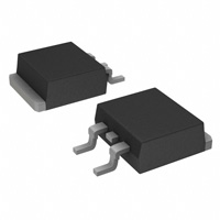
• Industry standard D2Pak package
• Lead-Free
C
VCES = 600V
VCE(on) typ. = 1.66V
G
@VGE = 15V, IC = 9.0A
E
n-channel
Benefits
• Generation 4 IGBTs offer highest efficiencies
available
• IGBTs optimized for specific application conditions
• HEXFRED diodes optimized for performance with
IGBTs . Minimized recovery characteristics require
less/no snubbing
• Designed to be a "drop-in" replacement for equivalent
industry-standard Generation 3 IR IGBTs
D 2 Pak
Absolute Maximum Ratings
Parameter
VCES
IC @ TC = 25°C
IC @ TC = 100°C
ICM
ILM
IF @ TC = 100°C
IFM
VGE
PD @ TC = 25°C
PD @ TC = 100°C
TJ
TSTG
Collector-to-Emitter Voltage
Continuous Collector Current
Continuous Collector Current
Pulsed Collector Current
Clamped Inductive Load Current
Diode Continuous Forward Current
Diode Maximum Forward Current
Gate-to-Emitter Voltage
Maximum Power Dissipation
Maximum Power Dissipation
Operating Junction and
Storage Temperature Range
Max.
Units
600
16
9.0
64
64
8.0
60
± 20
60
24
-55 to +150
V
A
V
W
°C
Thermal Resistance
Parameter
RθJC
RθJC
RθJA
Wt
Junction-to-Case - IGBT
Junction-to-Case - Diode
Junction-to-Ambient ( PCB Mounted,steady-state)*
Weight
Typ.
Max.
–––
–––
–––
1.44
2.1
3.5
80
–––
Units
°C/W
g (oz)
* When mounted on 1" square PCB (FR-4 or G-10 Material ). For recommended footprint and soldering techniques
refer to application note #AN-994.
www.irf.com
1
11/19/04
�IRG4BC20FD-SPbF
Electrical Characteristics @ TJ = 25°C (unless otherwise specified)
Parameter
Min. Typ.
Collector-to-Emitter Breakdown Voltage 600
—
∆V(BR)CES/∆TJ Temperature Coeff. of Breakdown Voltage —
0.72
VCE(on)
Collector-to-Emitter Saturation Voltage
— 1.66
— 2.06
— 1.76
Gate Threshold Voltage
3.0
—
VGE(th)
∆VGE(th)/∆TJ Temperature Coeff. of Threshold Voltage
—
-11
gfe
Forward Transconductance
2.9 5.1
Zero Gate Voltage Collector Current
—
—
ICES
—
—
VFM
Diode Forward Voltage Drop
—
1.4
—
1.3
IGES
Gate-to-Emitter Leakage Current
—
—
V(BR)CES
Max. Units
Conditions
—
V
VGE = 0V, IC = 250µA
—
V/°C VGE = 0V, I C = 1.0mA
2.0
IC = 9.0A
VGE = 15V
—
V
IC = 16A
See Fig. 2, 5
—
IC = 9.0A, TJ = 150°C
6.0
VCE = VGE, IC = 250µA
— mV/°C VCE = VGE, IC = 250µA
—
S
VCE = 100V, IC = 9.0A
250
µA
VGE = 0V, VCE = 600V
1700
VGE = 0V, VCE = 600V, TJ = 150°C
1.7
V
IC = 8.0A
See Fig. 13
1.6
IC = 8.0A, TJ = 150°C
±100 nA
VGE = ±20V
Switching Characteristics @ TJ = 25°C (unless otherwise specified)
Qg
Qge
Qgc
td(on)
tr
td(off)
tf
Eon
Eoff
Ets
td(on)
tr
td(off)
tf
Ets
LE
Cies
Coes
Cres
t rr
I rr
Q rr
di(rec)M/dt
2
Parameter
Total Gate Charge (turn-on)
Gate - Emitter Charge (turn-on)
Gate - Collector Charge (turn-on)
Turn-On Delay Time
Rise Time
Turn-Off Delay Time
Fall Time
Turn-On Switching Loss
Turn-Off Switching Loss
Total Switching Loss
Turn-On Delay Time
Rise Time
Turn-Off Delay Time
Fall Time
Total Switching Loss
Internal Emitter Inductance
Input Capacitance
Output Capacitance
Reverse Transfer Capacitance
Diode Reverse Recovery Time
Min.
—
—
—
—
—
—
—
—
—
—
—
—
—
—
—
—
—
—
—
—
—
Diode Peak Reverse Recovery Current —
—
Diode Reverse Recovery Charge
—
—
Diode Peak Rate of Fall of Recovery
—
During tb
—
Typ.
27
4.2
9.9
43
20
240
150
0.25
0.64
0.89
41
22
320
290
1.35
7.5
540
37
7.0
37
55
3.5
4.5
65
124
240
210
Max. Units
Conditions
40
IC = 9.0A
6.2
nC VCC = 400V
See Fig. 8
15
VGE = 15V
—
TJ = 25°C
—
ns
IC = 9.0A, VCC = 480V
360
VGE = 15V, RG = 50Ω
220
Energy losses include "tail" and
—
diode reverse recovery.
—
mJ See Fig. 9, 10, 18
1.3
—
TJ = 150°C, See Fig. 10, 11, 18
—
ns
IC = 9.0A, VCC = 480V
—
VGE = 15V, RG = 50Ω
—
Energy losses include "tail" and
—
mJ diode reverse recovery.
—
nH Measured 5mm from package
—
VGE = 0V
—
pF
VCC = 30V
See Fig. 7
—
ƒ = 1.0MHz
55
ns
TJ = 25°C See Fig.
90
TJ = 125°C
14
IF = 8.0A
5.0
A
TJ = 25°C See Fig.
8.0
TJ = 125°C
15
VR = 200V
138
nC TJ = 25°C See Fig.
360
TJ = 125°C
16
di/dt = 200A/µs
—
A/µs TJ = 25°C See Fig.
—
TJ = 125°C
17
www.irf.com
�IRG4BC20FD-SPbF
3.0
LOAD CURRENT (A)
For both: Mounted on PCB
Duty cycle: 50%
TJ = 125°C
55°C
Tsink = 90°C
Gate drive as specified
Power Dissipation = 1.75W
2.0
Square wave:
60% of rated
voltage
1.0
I
Ideal diodes
0.0
0.1
1
10
100
f, Frequency (KHz)
Fig. 1 - Typical Load Current vs. Frequency
(Load Current = IRMS of fundamental)
100
TJ = 25 o C
TJ = 150 o C
10
V GE = 15V
20µs PULSE WIDTH
1
1
10
VCE , Collector-to-Emitter Voltage (V)
Fig. 2 - Typical Output Characteristics
www.irf.com
I C, Collector-to-Emitter Current (A)
I C , Collector-to-Emitter Current (A)
100
TJ = 150 o C
10
TJ = 25 oC
V CC = 50V
5µs PULSE WIDTH
1
5
6
7
8
9
10
11
12
13
14
VGE , Gate-to-Emitter Voltage (V)
Fig. 3 - Typical Transfer Characteristics
3
�IRG4BC20FD-SPbF
3.0
VCE , Collector-to-Emitter Voltage(V)
Maximum DC Collector Current(A)
16
12
8
4
0
25
50
75
100
125
150
VGE = 15V
80 us PULSE WIDTH
IC = 18 A
2.0
A
IC = 9.0
9A
IC = 4.5 A
1.0
-60 -40 -20
TC , Case Temperature ( ° C)
0
20
40
60
80 100 120 140 160
TJ , Junction Temperature ( ° C)
Fig. 4 - Maximum Collector Current vs. Case
Temperature
Fig. 5 - Typical Collector-to-Emitter Voltage
vs. Junction Temperature
Thermal Response (Z thJC )
10
1
0.50
0.20
0.10
PDM
0.05
0.1
0.02
0.01
0.01
0.00001
t1
SINGLE PULSE
(THERMAL RESPONSE)
t2
Notes:
1. Duty factor D = t 1 / t 2
2. Peak TJ = PDM x Z thJC + TC
0.0001
0.001
0.01
0.1
1
t1 , Rectangular Pulse Duration (sec)
Fig. 6 - Maximum Effective Transient Thermal Impedance, Junction-to-Case
4
www.irf.com
�IRG4BC20FD-SPbF
1000
600
VGE , Gate-to-Emitter Voltage (V)
800
C, Capacitance (pF)
20
VGE = 0V,
f = 1MHz
Cies = Cge + Cgc , Cce SHORTED
Cres = Cgc
Coes = Cce + Cgc
Cies
400
200
Coes
VCC = 400V
I C = 9.0A
16
12
8
4
Cres
0
1
10
0
100
0
VCE , Collector-to-Emitter Voltage (V)
Total Switching Losses (mJ)
Total Switching Losses (mJ)
10
V CC = 480V
V GE = 15V
TJ = 25 ° C
0.88
I C = 9.0A
0.86
0.84
0.82
0.80
0.78
20
30
40
Ω
RG , Gate Resistance (Ohm)
Fig. 9 - Typical Switching Losses vs. Gate
Resistance
www.irf.com
15
20
25
30
Fig. 8 - Typical Gate Charge vs.
Gate-to-Emitter Voltage
0.90
10
10
QG , Total Gate Charge (nC)
Fig. 7 - Typical Capacitance vs.
Collector-to-Emitter Voltage
0
5
50
Ω
RG = 50Ohm
VGE = 15V
VCC = 480V
IC = 18 A
IC = 9.09 A
1
IC = 4.5 A
0.1
-60 -40 -20
0
20
40
60
80 100 120 140 160
TJ , Junction Temperature ( °C )
Fig. 10 - Typical Switching Losses vs.
Junction Temperature
5
�IRG4BC20FD-SPbF
100
= 50Ohm
Ω
= 150 ° C
= 480V
= 15V
I C , Collector-to-Emitter Current (A)
RG
TJ
VCC
2.5
VGE
2.0
1.5
1.0
0.5
VGE = 20V
T J = 125 oC
10
SAFE OPERATING AREA
1
0.0
0
4
8
12
16
20
1
10
100
1000
VCE , Collector-to-Emitter Voltage (V)
I C , Collector-to-emitter Current (A)
Fig. 11 - Typical Switching Losses vs.
Collector-to-Emitter Current
Fig. 12 - Turn-Off SOA
100
Instantaneous Forward Current - I F (A)
Total Switching Losses (mJ)
3.0
10
TJ = 150°C
TJ = 125°C
TJ = 25°C
1
0.1
0.4
0.8
1.2
1.6
2.0
2.4
2.8
3.2
Forward Voltage Drop - V FM (V)
Fig. 13 - Maximum Forward Voltage Drop vs. Instantaneous Forward Current
6
www.irf.com
�IRG4BC20FD-SPbF
100
100
VR = 200V
TJ = 125°C
TJ = 25°C
VR = 200V
TJ = 125°C
TJ = 25°C
80
60
I F = 8.0A
I IRRM - (A)
t rr - (ns)
IF = 16A
I F = 16A
10
IF = 8.0A
40
I F = 4.0A
I F = 4.0A
20
0
100
1
100
1000
di f /dt - (A/µs)
Fig. 14 - Typical Reverse Recovery vs. dif/dt
di f /dt - (A/µs)
1000
Fig. 15 - Typical Recovery Current vs. dif/dt
500
10000
VR = 200V
TJ = 125°C
TJ = 25°C
VR = 200V
TJ = 125°C
TJ = 25°C
di(rec)M/dt - (A/µs)
Q RR - (nC)
400
300
I F = 16A
200
I F = 8.0A
IF = 4.0A
1000
IF = 8.0A
I F = 16A
100
IF = 4.0A
0
100
di f /dt - (A/µs)
Fig. 16 - Typical Stored Charge vs. dif/dt
www.irf.com
1000
100
100
di f /dt - (A/µs)
1000
Fig. 17 - Typical di(rec)M/dt vs. dif/dt
7
�IRG4BC20FD-SPbF
Same type
device as
D.U.T.
430µF
80%
of Vce
90%
D.U.T.
10%
Vge
VC
90%
td(off)
10%
IC 5%
Fig. 18a - Test Circuit for Measurement of
tf
tr
ILM, Eon, Eoff(diode), trr, Qrr, Irr, td(on), tr, td(off), tf
t d(on)
t=5µs
Eon
Eoff
Ets= (Eon +Eoff )
Fig. 18b - Test Waveforms for Circuit of Fig. 18a, Defining
Eoff, td(off), tf
GATE VOLTAGE D.U.T.
10% +Vg
trr
Qrr =
Ic
∫
trr
id
Ic dtdt
tx
+Vg
tx
10% Irr
10% Vcc
Vcc
DUT VOLTAGE
AND CURRENT
Vce
Vpk
Irr
Vcc
10% Ic
90% Ic
Ipk
Ic
DIODE RECOVERY
WAVEFORMS
tr
td(on)
5% Vce
t1
∫
t2
VceieIcdt dt
Eon = Vce
t1
t2
DIODE REVERSE
RECOVERY ENERGY
t3
Fig. 18c - Test Waveforms for Circuit of Fig. 18a,
Defining Eon, td(on), tr
8
∫
t4
Erec = Vd
VdidIcdt dt
t3
t4
Fig. 18d - Test Waveforms for Circuit of Fig. 18a,
Defining Erec, trr, Qrr, Irr
www.irf.com
�IRG4BC20FD-SPbF
Vg GATE SIGNAL
DEVICE UNDER TEST
CURRENT D.U.T.
VOLTAGE IN D.U.T.
CURRENT IN D1
t0
t1
t2
Figure 18e. Macro Waveforms for Figure 18a's Test Circuit
D.U.T.
L
1000V
Vc*
RL=
0 - 480V
480V
4 X IC @25°C
50V
6000µF
100V
Figure 19. Clamped Inductive Load Test Circuit
www.irf.com
Figure 20. Pulsed Collector Current
Test Circuit
9
�IRG4BC20FD-SPbF
D2Pak Package Outline
Dimensions are shown in millimeters (inches)
D2Pak Part Marking Information
T HIS IS AN IRF530S WIT H
LOT CODE 8024
AS S EMBLED ON WW 02, 2000
IN T HE AS S EMBLY LINE "L"
INT ERNATIONAL
RECTIF IER
LOGO
Note: "P" in ass embly line
pos ition indicates "Lead-F ree"
PART NUMBER
F530S
AS S EMBLY
LOT CODE
OR
INTERNATIONAL
RECT IFIER
LOGO
ASS EMBLY
LOT CODE
10
DAT E CODE
YEAR 0 = 2000
WEEK 02
LINE L
PART NUMBER
F530S
DATE CODE
P = DESIGNATES LEAD-FREE
PRODUCT (OPT IONAL)
YEAR 0 = 2000
WEEK 02
A = AS SEMB LY S IT E CODE
www.irf.com
�IRG4BC20FD-SPbF
D2Pak Tape & Reel Information
Dimensions are shown in millimeters (inches)
TRR
1.60 (.063)
1.50 (.059)
4.10 (.161)
3.90 (.153)
FEED DIRECTION 1.85 (.073)
1.65 (.065)
1.60 (.063)
1.50 (.059)
11.60 (.457)
11.40 (.449)
0.368 (.0145)
0.342 (.0135)
15.42 (.609)
15.22 (.601)
24.30 (.957)
23.90 (.941)
TRL
10.90 (.429)
10.70 (.421)
1.75 (.069)
1.25 (.049)
4.72 (.136)
4.52 (.178)
16.10 (.634)
15.90 (.626)
FEED DIRECTION
13.50 (.532)
12.80 (.504)
27.40 (1.079)
23.90 (.941)
4
330.00
(14.173)
MAX.
60.00 (2.362)
MIN.
NOTES :
1. COMFORMS TO EIA-418.
2. CONTROLLING DIMENSION: MILLIMETER.
3. DIMENSION MEASURED @ HUB.
4. INCLUDES FLANGE DISTORTION @ OUTER EDGE.
26.40 (1.039)
24.40 (.961)
3
30.40 (1.197)
MAX.
4
Notes:
Repetitive rating: VGE=20V; pulse width limited by maximum junction temperature (figure
20)
VCC=80%(VCES), VGE=20V, L=10µH, RG = 50Ω (figure 19)
Pulse width ≤ 80µs; duty factor ≤ 0.1%.
Pulse width 5.0µs, single shot.
Data and specifications subject to change without notice.
IR WORLD HEADQUARTERS: 233 Kansas St., El Segundo, California 90245, USA Tel: (310) 252-7105
TAC Fax: (310) 252-7903
Visit us at www.irf.com for sales contact information. 11/04
www.irf.com
11
�Note: For the most current drawings please refer to the IR website at:
http://www.irf.com/package/
�