PD -95564A
IRG4BC20MD-SPbF
INSULATED GATE BIPOLAR TRANSISTOR WITH
ULTRAFAST SOFT RECOVERY DIODE
Features
• Rugged: 10µsec short circuit capable at VGS=15V
• Low VCE(on) for 4 to 10kHz applications
• IGBT Co-packaged with ultra-soft-recovery
antiparallel diode
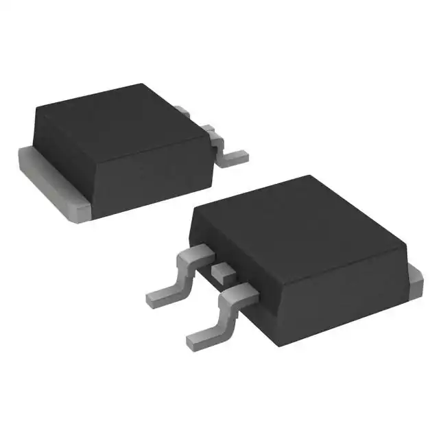
• Industry standard D2Pak package
• Lead-Free
C
VCES = 600V
VCE(on) typ. = 1.85V
G
Benefits
• Offers highest efficiency and short circuit
capability for intermediate applications
• Provides best efficiency for the mid range frequency
(4 to 10kHz)
• Optimized for Appliance Motor Drives, Industrial (Short
Circuit Proof) Drives and Intermediate Frequency
Range Drives
• High noise immune "Positive Only" gate driveNegative bias gate drive not necessary
• For Low EMI designs- requires little or no snubbing
• Single Package switch for bridge circuit applications
• Compatible with high voltage Gate Driver IC's
• Allows simpler gate drive
Short Circuit Rated
Fast IGBT
@VGE = 15V, IC = 11A
E
n-channel
D2 Pak
Absolute Maximum Ratings
Parameter
VCES
IC @ TC = 25°C
IC @ TC = 100°C
ICM
ILM
IF @ TC = 100°C
tsc
IFM
VGE
PD @ TC = 25°C
PD @ TC = 100°C
TJ
TSTG
Collector-to-Emitter Voltage
Continuous Collector Current
Continuous Collector Current
Pulsed Collector Current
Clamped Inductive Load Current
Diode Continuous Forward Current
Short Circuit Withstand Time
Diode Maximum Forward Current
Gate-to-Emitter Voltage
Maximum Power Dissipation
Maximum Power Dissipation
Operating Junction and
Storage Temperature Range
Soldering Temperature, for 10 sec.
Mounting Torque, 6-32 or M3 Screw.
Thermal Resistance
Parameter
RθJC
RθJC
RθCS
RθJA
Wt
www.irf.com
Junction-to-Case - IGBT
Junction-to-Case - Diode
Case-to-Sink, flat, greased surface
Junction-to-Ambient, typical socket mount
Weight
Max.
Units
600
18
11
36
36
7.0
10
36
± 20
60
24
-55 to +150
V
A
µs
A
V
W
°C
300 (0.063 in. (1.6mm) from case)
10 lbf•in (1.1 N•m)
Min.
Typ.
Max.
-------------------------
----------0.50
----2 (0.07)
2.1
2.5
-----80
------
Units
°C/W
g (oz)
1
01/19/10
�IRG4BC20MD-SPbF
Electrical Characteristics @ TJ = 25°C (unless otherwise specified)
Parameter
Min.
Collector-to-Emitter Breakdown Voltage 600
∆V(BR)CES/∆TJ Temperature Coeff. of Breakdown Voltage ---VCE(on)
Collector-to-Emitter Saturation Voltage ---------Gate Threshold Voltage
4.0
VGE(th)
∆VGE(th)/∆TJ Temperature Coeff. of Threshold Voltage ---gfe
Forward Transconductance
3.0
Zero Gate Voltage Collector Current
---ICES
---VFM
Diode Forward Voltage Drop
------IGES
Gate-to-Emitter Leakage Current
---V(BR)CES
Typ.
---0.67
1.85
2.46
2.07
----11
3.6
------1.4
1.3
----
Max. Units
Conditions
---V
VGE = 0V, IC = 250µA
---- V/°C VGE = 0V, I C = 1.0mA
2.1
IC = 11A
VGE = 15V
---V
IC = 18A
See Fig. 2, 5
---IC = 11A, TJ = 150°C
6.5
VCE = VGE, IC = 250µA
---- mV/°C VCE = VGE, IC = 250µA
---S
VCE = 100V, IC = 11A
250
µA
VGE = 0V, VCE = 600V
2500
VGE = 0V, VCE = 600V, TJ = 150°C
1.7
V
IC = 8.0A
See Fig. 13
1.6
IC = 8.0A, TJ = 150°C
±100 nA
VGE = ±20V
Switching Characteristics @ TJ = 25°C (unless otherwise specified)
Qg
Qge
Qgc
td(on)
tr
td(off)
tf
Eon
Eoff
Ets
td(on)
tr
td(off)
tf
Ets
LE
Cies
Coes
Cres
trr
Irr
Q rr
di(rec)M/dt
2
Parameter
Total Gate Charge (turn-on)
Gate - Emitter Charge (turn-on)
Gate - Collector Charge (turn-on)
Turn-On Delay Time
Rise Time
Turn-Off Delay Time
Fall Time
Turn-On Switching Loss
Turn-Off Switching Loss
Total Switching Loss
Turn-On Delay Time
Rise Time
Turn-Off Delay Time
Fall Time
Total Switching Loss
Internal Emitter Inductance
Input Capacitance
Output Capacitance
Reverse Transfer Capacitance
Diode Reverse Recovery Time
Min.
---------------------------------------------------------------Diode Peak Reverse Recovery Current ------Diode Reverse Recovery Charge
------Diode Peak Rate of Fall of Recovery
---During tb
----
Typ.
39
5.3
20
21
37
463
340
0.41
2.03
2.44
19
41
590
600
3.49
7.5
460
54
14
37
55
3.5
4.5
65
124
240
210
Max. Units
Conditions
59
IC = 11A
8.0
nC VCC = 400V
See Fig. 8
30
VGE = 15V
---TJ = 25°C
---ns
IC = 11A, VCC = 480V
690
VGE = 15V, RG = 50Ω
510
Energy losses include "tail" and
---diode reverse recovery.
---mJ See Fig. 9, 10, 11, 18
3.7
---TJ = 150°C, See Fig. 9, 10, 11, 18
---ns
IC = 6.5A, VCC = 480V
---VGE = 15V, RG = 50Ω
---Energy losses include "tail" and
---mJ diode reverse recovery.
---nH Measured 5mm from package
---VGE = 0V
---pF
VCC = 30V
See Fig. 7
---ƒ = 1.0MHz
55
ns
TJ = 25°C See Fig.
90
TJ = 125°C
14
IF = 8.0A
5.0
A
TJ = 25°C See Fig.
8.0
TJ = 125°C
15
VR = 200V
138
nC TJ = 25°C See Fig.
360
TJ = 125°C
16
di/dt 200A/µs
---- A/µs TJ = 25°C See Fig.
---TJ = 125°C
17
www.irf.com
�IRG4BC20MD-SPbF
Load Current ( A )
1.5
Duty cycle : 50%
Tj = 125°C
Tsink = 90°C
Gate drive as specified
Turn-on losses include effects of
reverse recovery
Power Dissipation = 13W
1.0
60% of rated
voltage
0.5
Ideal diodes
0.0
0.1
1
10
100
f , Frequency ( kHz )
Fig. 1 - Typical Load Current vs. Frequency
(Load Current = IRMS of fundamental)
IC , Collector-to Emitter Current (A)
10
1
T J = 150°C
TJ = 25°C
VGE= 15V
20µs PULSE WIDTH
0.1
0.1
1.0
VCE , Collector-to-Emitter Voltage (V)
Fig. 2 - Typical Output Characteristics
www.irf.com
10.0
I C , Collector-to-Emitter Current (A)
100
100
TJ = 150 °C
10
TJ = 25 °C
1
0.1
V CC = 50V
5µs PULSE WIDTH
6
8
10
12
14
16
VGE , Gate-to-Emitter Voltage (V)
Fig. 3 - Typical Transfer Characteristics
3
�IRG4BC20MD-SPbF
4.0
VCE , Collector-to Emitter Voltage (V)
Maximum DC Collector Current(A)
20
15
10
5
0
VGE = 15V
80µs PULSE WIDTH
IC = 22A
3.0
IC = 11A
2.0
IC = 5.5A
1.0
25
50
75
100
125
150
-60 -40 -20
TC , Case Temperature ( °C)
0
20
40
60
80 100 120 140
TJ , Junction Temperature (°C)
Fig. 4 - Maximum Collector Current vs.
Case Temperature
Fig. 5 - Typical Collector-to-Emitter Voltage
vs. Junction Temperature
Thermal Response (Z thJC )
10
1
D = 0.50
0.20
0.10
PDM
0.05
0.1
0.02
0.01
0.01
0.00001
t1
SINGLE PULSE
(THERMAL RESPONSE)
t2
Notes:
1. Duty factor D =t 1 / t2
2. Peak TJ = PDM x Z thJC + TC
0.0001
0.001
0.01
0.1
1
t1 , Rectangular Pulse Duration (sec)
Fig. 6 - Maximum IGBT Effective Transient Thermal Impedance, Junction-to-Case
4
www.irf.com
�IRG4BC20MD-SPbF
20
VGE = 0V,
f = 1MHz
Cies = Cge + Cgc , Cce SHORTED
Cres = Cgc
Coes = Cce + Cgc
VGE , Gate-to-Emitter Voltage (V)
C, Capacitance (pF)
800
600
Cies
400
200
Coes
VCC = 400V
I C = 11A
16
12
8
4
Cres
0
1
10
0
100
VCE , Collector-to-Emitter Voltage (V)
10
20
30
40
QG , Total Gate Charge (nC)
Fig. 7 - Typical Capacitance vs.
Collector-to-Emitter Voltage
Fig. 8 - Typical Gate Charge vs.
Gate-to-Emitter Voltage
2.5
100
VCC = 480V
VGE = 15V
TJ = 25°C
I C = 11A
Total Switching Losses (mJ)
Total Switching Losses (mJ)
0
2.4
2.3
RG = 50Ω
VGE = 15V
VCC = 480V
IC = 22A
10
IC = 11A
IC = 5.5A
1
0.1
0
10
20
30
40
RG, Gate Resistance (Ω)
Fig. 9 - Typical Switching Losses vs. Gate
Resistance
www.irf.com
50
-60 -40 -20
0
20
40
60
80 100 120 140 160
T J, Junction Temperature (°C)
Fig. 10 - Typical Switching Losses vs.
Junction Temperature
5
�IRG4BC20MD-SPbF
100
10.0
8.0
VCC = 480V
C, Capacitance(pF)
Total Switching Losses (mJ)
VGE = 20V
T J = 125°
RG = 50Ω
TJ = 150°C
VGE = 15V
6.0
4.0
SAFE OPERATING AREA
10
2.0
0.0
5
10
15
20
1
25
1
IC , Collector Current (A)
10
100
1000
VDS, Drain-to-Source Voltage (V)
Fig. 11 - Typical Switching Losses vs.
Collector-to-Emitter Current
Fig. 12 - Turn-Off SOA
Instantaneous Forward Current - I F (A)
100
10
TJ = 150°C
TJ = 125°C
TJ = 25°C
1
0.1
0.4
0.8
1.2
1.6
2.0
2.4
2.8
3.2
Forward Voltage Drop - V FM (V)
Fig. 13 - Maximum Forward Voltage Drop vs. Instantaneous Forward Current
6
www.irf.com
�IRG4BC20MD-SPbF
100
100
VR = 200V
TJ = 125°C
TJ = 25°C
VR = 200V
TJ = 125°C
TJ = 25°C
80
I F = 8.0A
I IRRM - (A)
t rr - (ns)
IF = 16A
60
I F = 16A
10
IF = 8.0A
40
I F = 4.0A
I F = 4.0A
20
0
100
1
100
1000
di f /dt - (A/µs)
Fig. 14 - Typical Reverse Recovery vs. dif/dt
di f /dt - (A/µs)
1000
Fig. 15 - Typical Recovery Current vs. dif/dt
500
10000
VR = 200V
TJ = 125°C
TJ = 25°C
VR = 200V
TJ = 125°C
TJ = 25°C
di(rec)M/dt - (A/µs)
Q RR - (nC)
400
300
I F = 16A
200
I F = 8.0A
1000
IF = 4.0A
IF = 8.0A
I F = 16A
100
IF = 4.0A
0
100
di f /dt - (A/µs)
Fig. 16 - Typical Stored Charge vs. dif/dt
www.irf.com
1000
100
100
di f /dt - (A/µs)
1000
Fig. 17 - Typical di(rec)M/dt vs. dif/dt
7
�IRG4BC20MD-SPbF
90% Vge
+Vge
Same type
device as
D.U.T.
Vce
Ic
90% Ic
10% Vce
Ic
5% Ic
430µF
80%
of Vce
D.U.T.
td(off)
tf
Eoff =
∫
t1+5µS
Vce ic dt
t1
Fig. 18a - Test Circuit for Measurement of
ILM, Eon, Eoff(diode), trr, Qrr, Irr, td(on), tr, td(off), tf
t1
t2
Fig. 18b - Test Waveforms for Circuit of Fig. 18a, Defining
Eoff, td(off), tf
GATE VOLTAGE D.U.T.
10% +Vg
trr
Ic
Qrr =
tx
DUT VOLTAGE
AND CURRENT
Vce
10% Ic
90% Ic
tr
td(on)
10% Irr
Ipk
Vpk
Vcc
Irr
Ic
DIODE RECOVERY
WAVEFORMS
5% Vce
t1
∫
t2
Eon = Vce ie dt
t1
t2
DIODE REVERSE
RECOVERY ENERGY
t3
Fig. 18c - Test Waveforms for Circuit of Fig. 18a,
Defining Eon, td(on), tr
8
∫
+Vg
10% Vcc
Vcc
trr
id dt
tx
∫
t4
Erec = Vd id dt
t3
t4
Fig. 18d - Test Waveforms for Circuit of Fig. 18a,
Defining Erec, trr, Qrr, Irr
www.irf.com
�IRG4BC20MD-SPbF
Vg GATE SIGNAL
DEVICE UNDER TEST
CURRENT D.U.T.
VOLTAGE IN D.U.T.
CURRENT IN D1
t0
t1
t2
Figure 18e. Macro Waveforms for Figure 18a's Test Circuit
RL = VCC
ICM
D.U.T.
L
1000V
Vc*
50V
6000µF
100V
0 - VCC
480µF
Pulsed Collector Current
Test Circuit
Figure 19. Clamped Inductive Load Test
Circuit
www.irf.com
Figure 20. Pulsed Collector Current
Test Circuit
9
�IRG4BC20MD-SPbF
D2Pak Package Outline
Dimensions are shown in millimeters (inches)
D2Pak Part Marking Information
7+,6�,6�$1�,5)���6�:,7+
3$57�180%(5
/27�&2' (�����
,17(51$7,21$/
$66(0%/('�21�::���������
5(& 7,),(5
)���6
/2*2
,1�7+(�$66( 0%/