PD - 95788B
IRG4BC40WSPbF
IRG4BC40WLPbF
INSULATED GATE BIPOLAR TRANSISTOR
Features
Designed expressly for Switch-Mode Power
Supply and PFC (power factor correction)
applications
Industry-benchmark switching losses improve
efficiency of all power supply topologies
50% reduction of Eoff parameter
Low IGBT conduction losses
Latest-generation IGBT design and construction offers
tighter parameters distribution, exceptional reliability
Lead-Free
C
VCES = 600V
VCE(on) typ. = 2.05V
G
@VGE = 15V, IC = 20A
E
n-channel
Benefits
Lower switching losses allow more cost-effective
operation than power MOSFETs up to 150 kHz
("hard switched" mode)
Of particular benefit to single-ended converters and
boost PFC topologies 150W and higher
Low conduction losses and minimal minority-carrier
recombination make these an excellent option for
resonant mode switching as well (up to >>300 kHz)
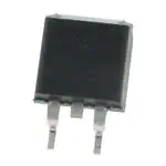
D2 Pak
IRG4BC40WSPbF
TO-262
IRG4BC40WLPbF
Absolute Maximum Ratings
VCES
IC @ TC = 25°C
IC @ TC = 100°C
ICM
ILM
VGE
EARV
PD @ TC = 25°C
PD @ TC = 100°C
TJ
TSTG
Parameter
Max.
Units
Collector-to-Emitter Breakdown Voltage
Continuous Collector Current
Continuous Collector Current
Pulsed Collector Current
Clamped Inductive Load Current
Gate-to-Emitter Voltage
Reverse Voltage Avalanche Energy
Maximum Power Dissipation
Maximum Power Dissipation
Operating Junction and
Storage Temperature Range
Soldering Temperature, for 10 seconds
600
40
20
160
160
± 20
160
160
65
-55 to + 150
V
A
V
mJ
W
300 (0.063 in. (1.6mm) from case )
°C
Thermal Resistance
Parameter
RθJC
RθCS
RθJA
Wt
www.irf.com
Junction-to-Case
Case-to-Sink, Flat, Greased Surface
Junction-to-Ambient (PCB Mounted steady-state)
Weight
Typ.
Max.
0.5
2.0 (0.07)
0.77
40
Units
°C/W
g (oz)
1
02/19/10
�IRG4BC40WS/LPbF
Electrical Characteristics @ TJ = 25°C (unless otherwise specified)
V(BR)CES
V(BR)ECS
∆V(BR)CES/∆TJ
VCE(ON)
VGE(th)
∆VGE(th)/∆TJ
gfe
ICES
IGES
Parameter
Min. Typ. Max. Units
Conditions
Collector-to-Emitter Breakdown Voltage
600
V
VGE = 0V, IC = 250µA
Emitter-to-Collector Breakdown Voltage 18
V
VGE = 0V, IC = 1.0A
Temperature Coeff. of Breakdown Voltage 0.44
V/°C VGE = 0V, IC = 1.0mA
2.05 2.5
IC = 20A
VGE = 15V
Collector-to-Emitter Saturation Voltage
2.36
IC = 40A
See Fig.2, 5
V
1.90
IC = 20A , TJ = 150°C
Gate Threshold Voltage
3.0
6.0
VCE = VGE, IC = 250µA
Temperature Coeff. of Threshold Voltage
13
mV/°C VCE = VGE, IC = 250µA
Forward Transconductance
18
28
S
VCE = 100 V, IC =20A
250
VGE = 0V, VCE = 600V
Zero Gate Voltage Collector Current
µA
2.0
VGE = 0V, VCE = 10V, TJ = 25°C
2500
VGE = 0V, VCE = 600V, TJ = 150°C
Gate-to-Emitter Leakage Current
±100
nA VGE = ±20V
Switching Characteristics @ TJ = 25°C (unless otherwise specified)
Qg
Qge
Qgc
t d(on)
tr
td(off)
tf
Eon
Eoff
E ts
td(on)
tr
t d(off)
tf
E ts
LE
Cies
Coes
Cres
Parameter
Total Gate Charge (turn-on)
Gate - Emitter Charge (turn-on)
Gate - Collector Charge (turn-on)
Turn-On Delay Time
Rise Time
Turn-Off Delay Time
Fall Time
Turn-On Switching Loss
Turn-Off Switching Loss
Total Switching Loss
Turn-On Delay Time
Rise Time
Turn-Off Delay Time
Fall Time
Total Switching Loss
Internal Emitter Inductance
Input Capacitance
Output Capacitance
Reverse Transfer Capacitance
Min.
Typ.
98
12
36
27
22
100
74
0.11
0.23
0.34
25
23
170
124
0.85
7.5
1900
140
35
Max. Units
Conditions
147
IC =20A
18
nC
VCC = 400V
See Fig.8
54
VGE = 15V
TJ = 25°C
ns
150
IC = 20A, VCC = 480V
110
VGE = 15V, RG = 10Ω
Energy losses include "tail"
mJ See Fig. 9,10, 14
0.45
TJ = 150°C,
IC = 20A, VCC = 480V
ns
VGE = 15V, RG = 10Ω
Energy losses include "tail"
mJ See Fig. 10,11, 14
nH
Measured 5mm from package
VGE = 0V
pF
VCC = 30V
See Fig. 7
= 1.0MHz
Notes:
Repetitive rating; VGE = 20V, pulse width limited by
max. junction temperature. ( See fig. 13b )
VCC = 80%(VCES), VGE = 20V, L = 10µH, RG = 10Ω,
(See fig. 13a)
Pulse width ≤ 80µs; duty factor ≤ 0.1%.
Pulse width 5.0µs, single shot.
Repetitive rating; pulse width limited by maximum
junction temperature.
2
www.irf.com
�IRG4BC40WS/LPbF
50
For both:
40
Load Current ( A )
Triangular wave:
Duty cycle: 50%
TJ = 125°C
Tsink = 90°C
Gate drive as specified
Power Dissipation = 28W
Clamp voltage:
80% of rated
30
Square wave:
60% of rated
voltage
20
10
Ideal diodes
A
0
0.1
1
10
100
1000
f, Frequency (kHz)
Fig. 1 - Typical Load Current vs. Frequency
(Load Current = IRMS of fundamental)
1000
TJ = 25 ° C
100
I C , Collector-to-Emitter Current (A)
I C , Collector-to-Emitter Current (A)
1000
100
TJ = 150 °C
10
V GE = 15V
80µs PULSE WIDTH
1
1.0
2.0
3.0
4.0
VCE , Collector-to-Emitter Voltage (V)
Fig. 2 - Typical Output Characteristics
www.irf.com
5.0
TJ = 150 °C
10
1
TJ = 25 °C
V CC = 50V
5µs PULSE WIDTH
5
7
9
11
VGE , Gate-to-Emitter Voltage (V)
Fig. 3 - Typical Transfer Characteristics
3
�IRG4BC40WS/LPbF
3.0
VCE , Collector-to-Emitter Voltage(V)
Maximum DC Collector Current(A)
50
40
30
20
10
0
25
50
75
100
125
150
TC , Case Temperature ( °C)
VGE = 15V
80 us PULSE WIDTH
IC = 40 A
2.5
IC = 20 A
2.0
IC = 10 A
1.5
1.0
-60 -40 -20
0
20
40
60
80 100 120 140 160
TJ , Junction Temperature ( ° C)
Fig. 4 - Maximum Collector Current vs. Case
Temperature
Fig. 5 - Typical Collector-to-Emitter Voltage
vs. Junction Temperature
Thermal Response (Z thJC )
1
D = 0.50
0.20
0.1
0.10
PDM
0.05
t1
0.02
0.01
0.01
0.00001
t2
SINGLE PULSE
(THERMAL RESPONSE)
0.0001
Notes:
1. Duty factor D = t 1 / t 2
2. Peak TJ = PDM x Z thJC + TC
0.001
0.01
0.1
1
t1 , Rectangular Pulse Duration (sec)
Fig. 6 - Maximum Effective Transient Thermal Impedance, Junction-to-Case
4
www.irf.com
�IRG4BC40WS/LPbF
VGE = 0V,
f = 1MHz
Cies = Cge + Cgc , Cce SHORTED
Cres = Cgc
Coes = Cce + Cgc
3000
Cies
2000
Coes
1000
0
Cres
1
10
20
VGE , Gate-to-Emitter Voltage (V)
C, Capacitance (pF)
4000
16
12
8
4
0
100
VCE , Collector-to-Emitter Voltage (V)
Total Switching Losses (mJ)
Total Switching Losses (mJ)
10
V CC = 480V
V GE = 15V
0.9 TJ = 25 °C
I C = 20A
0.8
0.7
0.6
0.5
0.4
20
30
40
50
RG , Gate Resistance (Ω)
(Ohm)
Fig. 9 - Typical Switching Losses vs. Gate
Resistance
www.irf.com
20
40
60
80
100
Fig. 8 - Typical Gate Charge vs.
Gate-to-Emitter Voltage
1.0
10
0
QG , Total Gate Charge (nC)
Fig. 7 - Typical Capacitance vs.
Collector-to-Emitter Voltage
0.3
VCC = 400V
I C = 20A
60
RG = 10
10Ohm
Ω
VGE = 15V
VCC = 480V
IC = 40 A
1
IC = 20 A
IC = 10 A
0.1
-60 -40 -20
0
20
40
60
80 100 120 140 160
TJ , Junction Temperature ( °C )
Fig. 10 - Typical Switching Losses vs.
Junction Temperature
5
�IRG4BC40WS/LPbF
RG
TJ
VCC
VGE
1000
Ω
= 10
10Ohm
= 150 ° C
= 480V
= 15V
I C , Collector-to-Emitter Current (A)
Total Switching Losses (mJ)
2.0
1.5
1.0
100
0.5
0.0
5
15
25
35
I C , Collector-to-emitter Current (A)
Fig. 11 - Typical Switching Losses vs.
Collector-to-Emitter Current
6
VGE = 20V
T J = 125 oC
45
10
SAFE OPERATING AREA
1
10
100
1000
VCE , Collector-to-Emitter Voltage (V)
Fig. 12 - Turn-Off SOA
www.irf.com
�IRG4BC40WS/LPbF
RL = VCC
ICM
L
D.U.T.
VC *
50V
1000V
0 - VCC
c
480µF
d
* Driver same type as D.U.T.; Vc = 80% of Vce(max)
* Note: Due to the 50V power supply, pulse width and inductor
will increase to obtain rated Id.
Pulsed Collector Current
Test Circuit
Fig. 13a - Clamped Inductive
Fig. 13b - Pulsed Collector
Load Test Circuit
Current Test Circuit
IC
L
Driver*
D.U.T.
VC
Test Circuit
50V
1000V
c�
Fig. 14a - Switching Loss
d
e
* Driver same type
as D.U.T., VC = 480V
c
d
90%
e
VC
10%
90%
Fig. 14b - Switching Loss
t d(off)
10%
I C 5%
Waveforms
tf
tr
t d(on)
t=5µs
E on
E off
E ts = (Eon +Eoff )
www.irf.com
7
�IRG4BC40WS/LPbF
D2Pak Package Outline
Dimensions are shown in millimeters (inches)
D2Pak Part Marking Information
7+,6�,6�$1�,5)���6�:,7+
/27�&2'(�����
$66(0%/('�21�::���������
,1�7+(�$66(0%/