PD 91735A
IRG4RC10K
Short Circuit Rated
UltraFast IGBT
INSULATED GATE BIPOLAR TRANSISTOR
Features
C
• Short Circuit Rated UltraFast: Optimized for high
operating frequencies >5.0 kHz , and Short Circuit
Rated to 10µs @ 125°C, VGE = 15V
• Generation 4 IGBT design provides higher efficiency
than Generation 3
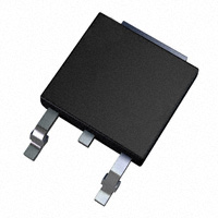
• Industry standard TO-252AA package
VCES = 600V
VCE(on) typ. = 2.39V
G
@VGE = 15V, IC = 5.0A
E
n-channel
Benefits
• Generation 4 IGBT's offer highest efficiency available
• IGBT's optimized for specified application conditions
D-PAK
TO-252AA
Absolute Maximum Ratings
VCES
IC @ TC = 25°C
IC @ TC = 100°C
ICM
ILM
tsc
VGE
EARV
PD @ T C = 25°C
PD @ T C = 100°C
TJ
TSTG
Parameter
Max.
Units
Collector-to-Emitter Breakdown Voltage
Continuous Collector Current
Continuous Collector Current
Pulsed Collector Current�Q
Clamped Inductive Load Current�R
Short Circuit Withstand Time
Gate-to-Emitter Voltage
Reverse Voltage Avalanche Energy S
Maximum Power Dissipation
Maximum Power Dissipation
Operating Junction and
Storage Temperature Range
Soldering Temperature, for 10 seconds
600
9.0
5.0
18
18
10
± 20
34
38
15
-55 to + 150
V
A
µs
V
mJ
W
°C
300 (0.063 in. (1.6mm) from case )
Thermal Resistance
Parameter
RθJC
RθJA
Wt
Junction-to-Case
Junction-to-Ambient (PCB mount)*
Weight
Typ.
Max.
–––
–––
0.3 (0.01)
3.3
50
–––
Units
°C/W
g (oz)
* When mounted on 1" square PCB (FR-4 or G-10 Material).
For recommended footprint and soldering techniques refer to application note #AN-994
www.irf.com
1
12/30/00
�IRG4RC10K
Electrical Characteristics @ TJ = 25°C (unless otherwise specified)
V(BR)CES
V(BR)ECS
∆V(BR)CES/∆TJ
VCE(ON)
VGE(th)
∆VGE(th)/∆TJ
gfe
ICES
IGES
Parameter
Min. Typ.
Collector-to-Emitter Breakdown Voltage
600
—
Emitter-to-Collector Breakdown Voltage T 18
—
Temperature Coeff. of Breakdown Voltage — 0.58
— 2.39
Collector-to-Emitter Saturation Voltage
— 3.25
— 2.63
Gate Threshold Voltage
3.0
—
Temperature Coeff. of Threshold Voltage
—
-11
Forward Transconductance U
1.2
1.8
—
—
Zero Gate Voltage Collector Current
—
—
—
—
Gate-to-Emitter Leakage Current
—
—
Max. Units
Conditions
—
V
VGE = 0V, IC = 250µA
—
V
VGE = 0V, IC = 1.0A
—
V/°C VGE = 0V, IC = 1.0mA
VGE = 15V
2.62
IC = 5.0A
—
IC = 9.0A
See Fig.2, 5
V
—
IC = 5.0A , TJ = 150°C
6.5
VCE = VGE, IC = 250µA
— mV/°C VCE = VGE, IC = 250µA
—
S
VCE = 50 V, IC = 5.0A
250
VGE = 0V, VCE = 600V
µA
2.0
VGE = 0V, VCE = 10V, TJ = 25°C
1000
VGE = 0V, VCE = 600V, TJ = 150°C
±100
nA
VGE = ±20V
Switching Characteristics @ TJ = 25°C (unless otherwise specified)
Qg
Qge
Qgc
td(on)
tr
td(off)
tf
Eon
Eoff
Ets
tsc
td(on)
tr
td(off)
tf
Ets
LE
Cies
Coes
Cres
Notes:
Parameter
Total Gate Charge (turn-on)
Gate - Emitter Charge (turn-on)
Gate - Collector Charge (turn-on)
Turn-On Delay Time
Rise Time
Turn-Off Delay Time
Fall Time
Turn-On Switching Loss
Turn-Off Switching Loss
Total Switching Loss
Short Circuit Withstand Time
Min.
—
—
—
—
—
—
—
—
—
—
10
Turn-On Delay Time
Rise Time
Turn-Off Delay Time
Fall Time
Total Switching Loss
Internal Emitter Inductance
Input Capacitance
Output Capacitance
Reverse Transfer Capacitance
Q Repetitive rating; VGE = 20V, pulse width limited by
max. junction temperature. ( See fig. 13b )
R VCC = 80%(VCES), VGE = 20V, L = 10µH, RG = 100Ω,
(See fig. 13a)
2
—
—
—
—
—
—
—
—
—
Typ. Max. Units
Conditions
19
29
IC = 5.0A
2.9 4.3
nC
VCC = 400V
See Fig.8
9.8
15
VGE = 15V
11
—
24
—
TJ = 25°C
ns
51
77
IC = 5.0A, VCC = 480V
190 290
VGE = 15V, R G = 100Ω
0.16 —
Energy losses include "tail"
0.10 —
mJ See Fig. 9,10,14
0.26 0.32
—
—
µs
VCC = 400V, TJ = 125°C
VGE = 15V, R G = 100Ω , VCPK < 500V
11
—
TJ = 150°C,
27
—
IC = 5.0A, VCC = 480V
ns
67
—
VGE = 15V, R G = 100Ω
350
—
Energy losses include "tail"
0.47 —
mJ See Fig. 10,11,14
7.5
—
nH
Measured 5mm from package
220
—
VGE = 0V
29
—
pF
VCC = 30V
See Fig. 7
7.5
—
ƒ = 1.0MHz
S Repetitive rating; pulse width limited by maximum
junction temperature.
T Pulse width ≤ 80µs; duty factor ≤ 0.1%.
U Pulse width 5.0µs, single shot.
www.irf.com
�IRG4RC10K
4
For both:
3
Loa d C urre nt (A )
Triangular wave:
Duty cycle: 50%
TJ = 125°C
Tsink = 55°C
Gate drive as specified
Power Dissipation = 1.4W
Clamp voltage:
80% of rated
Square wave:
2
60% of rated
voltage
1
Ideal diodes
A
0
0.1
1
10
100
f, F re q u e n c y (k H z)
Fig. 1 - Typical Load Current vs. Frequency
(Load Current = IRMS of fundamental)
100
TJ = 25 °C
�
10
TJ = 150 °C
�
V
= 15V
�
20µs PULSE WIDTH
I C , Collector-to-Emitter Current (A)
I C , Collector Current (A)
100
10
TJ = 150 °C
�
TJ = 25 °C
�
GE
1
1.0
2.0
3.0
4.0
5.0
6.0
7.0
VCE , Collector-to-Emitter Voltage (V)
Fig. 2 - Typical Output Characteristics
www.irf.com
1
5
10
V
= 50V
�
5µs PULSE WIDTH
CC
15
20
VGE , Gate-to-Emitter Voltage (V)
Fig. 3 - Typical Transfer Characteristics
5µs PULSE WIDTH
3
�IRG4RC10K
5.0
V
= 15V
�
80 us PULSE WIDTH
GE
VCE , Collector-to-Emitter Voltage(V)
Maximum DC Collector Current(A)
10
8
6
4
2
0
25
50
75
100
125
150
�
I C = 10 A
4.0
3.0
�
IC = 5 A
�
I C = 2.5 A
2.0
1.0
-60 -40 -20
0
20
40
60
80 100 120 140 160
TJ , Junction Temperature ( ° C)
TC , Case Temperature ( °C)
Fig. 4 - Maximum Collector Current vs. Case
Temperature
Fig. 5 - Typical Collector-to-Emitter Voltage
vs. Junction Temperature
Thermal Response (Z thJC )
10
D = 0.50
1
0.20
0.10
�
0.05
0.1
0.01
0.00001
0.02
0.01
P DM
SINGLE PULSE
�
(THERMAL RESPONSE)
t1
t2
�
Notes:
1. Duty factor D = t 1 / t 2
2. Peak TJ = PDM x Z thJC + TC
0.0001
0.001
0.01
0.1
1
t1 , Rectangular Pulse Duration (sec)
Fig. 6 - Maximum Effective Transient Thermal Impedance, Junction-to-Case
4
www.irf.com
�IRG4RC10K
VGE = 0V,
f = 1MHz
Cies = Cge + Cgc , Cce SHORTED
Cres = Cgc
Coes = Cce + Cgc
C, Capacitance (pF)
300
Cies
�
200
100
C�
oes
20
VGE , Gate-to-Emitter Voltage (V)
�
400
�
VCC = 400V
I C = 5.0A
16
12
8
4
Cres
�
0
1
10
0
100
0
VCE , Collector-to-Emitter Voltage (V)
�
10
VCC = 480V
VGE = 15V
TJ = 25 °C
I C = 5A
Total Switching Losses (mJ)
Total Switching Losses (mJ)
0.26
0.24
0.22
0.20
0
20
40
60
80
RG , Gate Resistance ( Ω )
Fig. 9 - Typical Switching Losses vs. Gate
Resistance
www.irf.com
8
12
16
20
Fig. 8 - Typical Gate Charge vs.
Gate-to-Emitter Voltage
Fig. 7 - Typical Capacitance vs.
Collector-to-Emitter Voltage
0.28
4
QG , Total Gate Charge (nC)
100
�
100Ω
RG = Ohm
VGE = 15V
VCC = 480V
�
IC = 10 A
1
�
IC = 5 A
�
IC = 2.5 A
0.1
-60 -40 -20
0
20
40
60
80 100 120 140 160
TJ , Junction Temperature ( °C )
Fig. 10 - Typical Switching Losses vs.
Junction Temperature
5
�IRG4RC10K
�
RG
TJ
VCC
1.0 VGE
�
100
= 100
OhmΩ
= 150 ° C
= 480V
= 15V
I C , Collector Current (A)
Total Switching Losses (mJ)
1.2
0.8
0.6
VGE = 20V
T J = 125 oC
10
0.4
�SAFE OPERATING AREA
1
0.2
2
4
6
8
1
10
10
Fig. 11 - Typical Switching Losses vs.
Collector Current
L
1000
Fig. 12 - Turn-Off SOA
D .U .T.
VC *
50V
100
VCE , Collector-to-Emitter Voltage (V)
I C , Collector Current (A)
RL =
0 - 480V
10 0 0V
480V
4 X I C@25°C
480µF
960V
Q
R
* Driver s am e ty pe a s D .U .T .; V c = 80 % of Vc e(m ax )
* Note: Due to the 5 0V pow e r supply, puls e w idth and inductor
w ill incre as e to obta in rated Id.
Fig. 13a - Clamped Inductive
Fig. 13b - Pulsed Collector
Load Test Circuit
Current Test Circuit
IC
L
D river*
D .U .T.
VC
Fig. 14a - Switching Loss
Test Circuit
50V
1000V
Q�
* Driver same type
as D.U.T., VC = 480V
R
6
S
www.irf.com
�IRG4RC10K
Q
R
90 %
10 %
S
VC
90 %
Fig. 14b - Switching Loss
t d (o ff)
1 0%
IC 5%
Waveforms
tf
tr
t d (o n )
t=5µ s
Eon
E o ff
E ts = (E o n +E o ff )
Package Outline
TO-252AA Outline
Dimensions are shown in millimeters (inches)
2 .3 8 (.09 4)
2 .1 9 (.08 6)
6.73 (.2 65)
6.35 (.2 50)
-A1.2 7 (.050 )
0.8 8 (.035 )
5.46 (.2 15 )
5.21 (.2 05 )
1.14 (.0 45)
0.89 (.0 35)
0.5 8 (.02 3)
0.4 6 (.01 8)
4
6.45 (.2 45 )
5.68 (.2 24 )
6.2 2 (.245 )
5.9 7 (.235 )
1.02 (.0 40)
1.64 (.0 25)
1
2
1 0.42 (.4 10 )
9 .4 0 (.37 0)
0.51 (.0 20 )
M IN.
-B1.5 2 (.0 60 )
1.1 5 (.0 45 )
3X
1 .1 4 (.04 5)
2 X 0 .7 6 (.03 0)
0.8 9 (.035 )
0.6 4 (.025 )
0 .25 (.01 0)
2 .28 (.09 0)
4.5 7 (.1 80 )
www.irf.com
LEAD ASSIGNMENTS
3
M A M B
LE AD A1SS
IG N M E NTS
- GATE
1 - G ATE
2 - COLLECTOR
2 - D RA IN
3 - EMITTER
3 - SO U R C E
COLLECTOR
44
- D- RA
IN
0 .58 (.0 23)
0 .46 (.0 18)
N O TE S:
1 D IM EN S IO N IN G & TO LE R AN C IN G PE R A N SI Y 14 .5M , 1 982 .
2 C O N TR O LLING D IM EN S IO N : INC H .
3 C O N FO R M S TO JED E C O U TLIN E TO -25 2A A.
4 D IM EN S IO N S S H O W N AR E B EF O RE SO L D ER D IP,
SO L D ER D IP M AX. +0 .16 (.00 6).
7
�IRG4RC10K
Tape & Reel Information
TO-252AA
TR
TRR
1 6.3 ( .641 )
1 5.7 ( .619 )
12 .1 ( .4 76 )
11 .9 ( .4 69 )
F E E D D IR E C T IO N
TRL
16 .3 ( .641 )
15 .7 ( .619 )
8.1 ( .318 )
7.9 ( .312 )
F E E D D IR E C T IO N
NO T ES :
1. C O N T R O LL IN G D IM E N S IO N : M ILLIM E T E R .
2. A LL D IM E N S IO N S A R E S H O W N IN M ILL IM E T E R S ( IN C H E S ).
3. O U T L IN E C O N F O R M S T O E IA -4 81 & E IA -54 1.
13 IN C H
16 m m
NOTES :
1. O U T LIN E C O N F O R M S T O E IA -481 .
IR WORLD HEADQUARTERS: 233 Kansas St., El Segundo, California 90245, USA Tel: (310) 252-7105
TAC Fax: (310) 252-7903
Visit us at www.irf.com for sales contact information.
Data and specifications subject to change without notice. 12/00
8
www.irf.com
�Note: For the most current drawings please refer to the IR website at:
http://www.irf.com/package/
�