IRG7PH28UD1PbF
IRG7PH28UD1MPbF
INSULATED GATE BIPOLAR TRANSISTOR WITH ULTRA-LOW VF DIODE
FOR INDUCTION HEATING AND SOFT SWITCHING APPLICATIONS
Features
Low VCE (ON) trench IGBT technology
Low switching losses
Square RBSOA
Ultra-low VF diode
1300Vpk repetitive transient capacity
100% of the parts tested for ILM
Positive VCE (ON) temperature co-efficient
Tight parameter distribution
Lead-free package
Package Type
IRG7PH28UD1PbF
IRG7PH28UD1MPbF
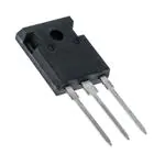
TO-247AC
TO-247AD
1
www.irf.com
© 2012 International Rectifier
TJ(MAX) = 150°C
VCE(ON) typ. = 1.95V
E
n-channel
G
G
C
G
IRG7PH28UD1PbF
TO-247AC
G
Gate
Tube
Tube
E
C
G
25
25
E
IRG7PH28UD1MPbF
TO-247AD
C
Collector
Standard Pack
Form
Quantity
Parameter
Collector-to-Emitter Voltage
Repetitive Transient Collector-to-Emitter Voltage
Continuous Collector Current
Continuous Collector Current
Pulse Collector Current, VGE = 15V
Clamped Inductive Load Current, VGE = 20V
Diode Continuous Forward Current
Diode Continuous Forward Current
Diode Maximum Forward Current
Continuous Gate-to-Emitter Voltage
Maximum Power Dissipation
Maximum Power Dissipation
Operating Junction and
Storage Temperature Range
Soldering Temperature, for 10 sec.
Mounting Torque, 6-32 or M3 Screw
VCES = 1200V
G
Absolute Maximum Ratings
VCES
V(BR) Transient
IC @ TC = 25°C
IC @ TC = 100°C
ICM
ILM
IF @ TC = 25°C
IF @ TC = 100°C
IFM
VGE
PD @ TC = 25°C
PD @ TC = 100°C
TJ
TSTG
IC = 15A, TC = 100°C
Benefits
Device optimized for induction heating and soft switching
applications
High efficiency due to low VCE(ON), low switching losses and
ultra-low VF
Rugged transient performance for increased reliability
Excellent current sharing in parallel operation
Low EMI
Base part number
C
E
Emitter
Orderable Part Number
IRG7PH28UD1PbF
IRG7PH28UD1MPbF
Max.
1200
1300
30
15
100
60
30
15
60
±30
115
46
-55 to +150
Units
V
A
V
W
°C
300
(0.063 in.(1.6mm) from case)
10 lbf·in (1.1 N·m)
January 8, 2013
�IRG7PH28UD1PbF/IRG7PH28UD1MPbF
Thermal Resistance
Parameter
Min.
–––
–––
–––
–––
RθJC (IGBT) Junction-to-Case (IGBT)
RθJC (Diode) Junction-to-Case (Diode)
RθCS
Case-to-Sink (flat, greased surface)
Junction-to-Ambient (typical socket mount)
RθJA
Electrical Characteristics @ TJ = 25°C (unless otherwise specified)
Parameter
Min.
Typ.
Collector-to-Emitter Breakdown Voltage
1200
—
V(BR)CES
—
1.4
V(BR)CES/TJ Temperature Coeff. of Breakdown Voltage
VCE(on)
Collector-to-Emitter Saturation Voltage
—
1.95
—
2.4
VGE(th)
Gate Threshold Voltage
3.0
—
gfe
Forward Transconductance
—
13
ICES
Collector-to-Emitter Leakage Current
—
1.0
—
100
VFM
Diode Forward Voltage Drop
—
1.1
—
1.0
IGES
Gate-to-Emitter Leakage Current
—
—
Switching Characteristics @ TJ = 25°C (unless otherwise specified)
Parameter
Min.
Typ.
Total Gate Charge (turn-on)
—
60
Qg
Qge
Gate-to-Emitter Charge (turn-on)
—
10
Gate-to-Collector Charge (turn-on)
—
27
Qgc
Turn-Off Switching Loss
—
543
Eoff
td(off)
tf
Eoff
Turn-Off delay time
Fall time
Turn-Off Switching Loss
—
—
—
td(off)
tf
Cies
Coes
Cres
Turn-Off delay time
Fall time
Input Capacitance
Output Capacitance
Reverse Transfer Capacitance
—
—
—
—
—
RBSOA
Reverse Bias Safe Operating Area
Max. Units
—
V
—
V/°C
2.30
V
—
6.0
V
—
S
100
µA
—
1.2
V
—
±100
nA
Typ.
–––
–––
0.24
–––
Max.
1.09
1.35
–––
40
Units
°C/W
Conditions
VGE = 0V, IC = 100µA
VGE = 0V, IC = 1mA (25°C-150°C)
IC = 15A, VGE = 15V, TJ = 25°C
IC = 15A, VGE = 15V, TJ = 150°C
VCE = VGE, IC = 350µA
VCE = 50V, IC = 15A, PW = 20µs
VGE = 0V, VCE = 1200V
VGE = 0V, VCE = 1200V, TJ = 150°C
IF = 15A
IF = 15A, TJ = 150°C
VGE = ±30V
Max. Units
Conditions
90
IC = 15A
nC VGE = 15V
15
VCC = 600V
40
766
µJ
IC = 15A, VCC = 600V, VGE = 15V
RG = 22, L = 1.0mH, TJ = 25°C
229
—
ns Energy losses include tail & diode
reverse recovery
62
—
939
—
µJ
IC = 15A, VCC = 600V, VGE=15V
RG = 22, L = 1.0mH, TJ = 150°C
Energy losses include tail & diode
272
—
ns
reverse recovery
167
—
1160
—
VGE = 0V
pF VCC = 30V
55
—
f = 1.0Mhz
30
—
TJ = 150°C, IC = 60A
FULL SQUARE
VCC = 960V, Vp ≤ 1200V
Rg = 22, VGE = +20V to 0V
Notes:
VCC = 80% (VCES), VGE = 20V, L = 25µH, RG = 22.
Pulse width limited by max. junction temperature.
Refer to AN-1086 for guidelines for measuring V(BR)CES safely.
R is measured at TJ of approximately 90°C.
FBSOA operating conditions only.
VGE = 0V, TJ = 75°C, PW ≤ 10µs.
2
www.irf.com
© 2012 International Rectifier
January 8, 2013
�IRG7PH28UD1PbF/IRG7PH28UD1MPbF
30
120
25
100
20
80
Ptot (W)
IC (A)
15
60
10
40
5
20
0
0
25
50
75
100
125
25
150
50
75
4.2
100
IC = 350µA
4.0
3.8
3.6
IC (A)
V GE(th), Gate Threshold Voltage
150
Fig. 2 - Power Dissipation vs.
Case Temperature
Fig. 1 - Maximum DC Collector Current vs.
Case Temperature
3.4
10
3.2
3.0
2.8
2.6
1
25
50
75
100
125
10
150
100
60
60
50
50
ICE (A)
V GE = 15V
V GE = 12V
V GE = 10V
20
V GE = 18V
40
V GE = 18V
30
10000
Fig. 4 - Reverse Bias SOA
TJ = 150°C; VGE = 20V
Fig. 3 - Typical Gate Threshold Voltage
vs. Junction Temperature
40
1000
V CE (V)
TJ , Temperature (°C)
ICE (A)
125
TC (°C)
TC (°C)
V GE = 15V
V GE = 12V
30
V GE = 10V
V GE = 8.0V
20
V GE = 8.0V
10
10
0
0
0
3
100
2
4
6
8
10
0
2
4
6
8
10
V CE (V)
V CE (V)
Fig. 5 - Typ. IGBT Output Characteristics
TJ = -40°C; tp = 20µs
Fig. 6 - Typ. IGBT Output Characteristics
TJ = 25°C; tp = 20µs
www.irf.com
© 2012 International Rectifier
January 8, 2013
�IRG7PH28UD1PbF/IRG7PH28UD1MPbF
60
100
V GE = 18V
V GE = 15V
50
V GE = 12V
40
V GE = 10V
10
IF (A)
ICE (A)
V GE = 8.0V
30
20
1
25°C
150°C
10
0
0.1
0
2
4
6
8
10
0.2
0.4
0.6
0.8
V CE (V)
12
10
10
ICE = 7.5A
ICE = 15A
V CE (V)
V CE (V)
8
ICE = 30A
1.8
ICE = 30A
4
2
2
0
5
10
15
20
5
10
Fig. 9 - Typical VCE vs. VGE
TJ = -40°C
70
10
60
ICE = 7.5A
ICE = 15A
50
ICE = 30A
40
ICE (A)
6
20
Fig. 10 - Typical VCE vs. VGE
TJ = 25°C
12
8
15
V GE (V)
V GE (V)
V CE (V)
1.6
ICE = 7.5A
ICE = 15A
6
4
0
4
30
TJ = 150°C
20
2
TJ = 25°C
10
0
0
5
4
1.4
Fig. 8 - Typ. Diode Forward Voltage Drop
Characteristics
12
6
1.2
VF (V)
Fig. 7 - Typ. IGBT Output Characteristics
TJ = 150°C; tp = 20µs
8
1.0
10
15
20
4
5
6
7
8
9
10
11
12
V GE (V)
V GE (V)
Fig. 11 - Typical VCE vs. VGE
TJ = 150°C
Fig. 12 - Typ. Transfer Characteristics
VCE = 50V; tp = 20µs
www.irf.com
© 2012 International Rectifier
January 8, 2013
�IRG7PH28UD1PbF/IRG7PH28UD1MPbF
1000
2000
tdOFF
Swiching Time (ns)
Energy (µJ)
1600
EOFF
1200
800
tF
100
400
10
0
0
5
10
15
20
25
0
30
5
10
15
IC (A)
Fig. 13 - Typ. Energy Loss vs. IC
TJ = 150°C; L = 1.0mH; VCE = 600V, RG = 22; VGE = 15V
25
30
Fig. 14 - Typ. Switching Time vs. IC
TJ = 150°C; L = 1.0mH; VCE = 600V, RG = 22; VGE = 15V
1000
1800
tdOFF
1600
Swiching Time (ns)
EOFF
1400
Energy (µJ)
20
IC (A)
1200
tF
100
1000
10
800
0
20
40
60
80
0
100
20
40
Fig. 15 - Typ. Energy Loss vs. RG
TJ =
100
Fig. 16 - Typ. Switching Time vs. RG
TJ = 150°C; L = 1.0mH; VCE = 600V, ICE = 15A; VGE = 15V
10000
V GE, Gate-to-Emitter Voltage (V)
16
Cies
1000
Capacitance (pF)
80
RG ( )
Rg ()
100
Coes
Cres
10
14
V CES = 600V
12
V CES = 400V
10
8
6
4
2
0
1
0
5
60
100
200
300
400
500
600
0
10
20
30
40
50
60
70
V CE (V)
Q G, Total Gate Charge (nC)
Fig. 17 - Typ. Capacitance vs. VCE
VGE= 0V; f = 1MHz
Fig. 18 - Typical Gate Charge vs. VGE
ICE = 15A
www.irf.com
© 2012 International Rectifier
January 8, 2013
�IRG7PH28UD1PbF/IRG7PH28UD1MPbF
Thermal Response ( Z thJC )
10
1
D = 0.50
0.20
0.1
0.01
0.10
0.05
0.02
0.01
J
0.0001
1E-006
1E-005
J
1
R2
R2
R3
R3
R4
R4
C
2
1
2
3
4
3
C
4
Ci= iRi
Ci= iRi
SINGLE PULSE
( THERMAL RESPONSE )
0.001
R1
R1
Ri (°C/W)
i (sec)
0.015352
0.000008
0.360775
0.000223
0.431394
0.002475
0.282479
0.01715
Notes:
1. Duty Factor D = t1/t2
2. Peak Tj = P dm x Zthjc + Tc
0.0001
0.001
0.01
0.1
1
t1 , Rectangular Pulse Duration (sec)
Fig. 19 - Maximum Transient Thermal Impedance, Junction-to-Case (IGBT)
Thermal Response ( Z thJC )
10
1
D = 0.50
0.20
0.10
0.1
0.05
J
0.02
0.01
R1
R1
J
1
R2
R2
R3
R3
R4
R4
C
2
1
2
3
4
3
Ci= iRi
Ci= iRi
0.01
1E-005
0.0001
i (sec)
0.00756
0.000005
0.56517
0.000677
0.54552
0.003514
0.25085
0.019551
Notes:
1. Duty Factor D = t1/t2
2. Peak Tj = P dm x Zthjc + Tc
SINGLE PULSE
( THERMAL RESPONSE )
0.001
1E-006
4
C
Ri (°C/W)
0.001
0.01
0.1
1
t1 , Rectangular Pulse Duration (sec)
Fig. 20 - Maximum Transient Thermal Impedance, Junction-to-Case (DIODE)
6
www.irf.com
© 2012 International Rectifier
January 8, 2013
�IRG7PH28UD1PbF/IRG7PH28UD1MPbF
L
L
0
80 V +
VCC
DUT
-
DUT
1K
VCC
Rg
Fig.C.T.2 - RBSOA Circuit
Fig.C.T.1 - Gate Charge Circuit (turn-off)
diode clamp /
DUT
C force
L
100K
D1
-5V
22K
C sense
DUT /
DRIVER
VCC
DUT
G force
0.0075µF
Rg
E sense
E force
Switching Loss
Fig.C.T.3 - Switching Loss Circuit
Fig.C.T.4 - BVCES Filter Circuit
40
800
tf
700
35
30
600
VCE (V)
90% ICE
400
20
300
15
200
10
100
5% ICE
5
5% VCE
0
0
Eoff Loss
-100
-0.5
ICE (A)
25
500
0
0.5
-5
1
time(µs)
Fig. WF1 - Typ. Turn-off Loss Waveform
@ TJ = 150°C using Fig. CT.3
7
www.irf.com
© 2012 International Rectifier
January 8, 2013
�IRG7PH28UD1PbF/IRG7PH28UD1MPbF
TO-247AC Package Outline
Dimensions are shown in millimeters (inches)
TO-247AC Part Marking Information
Notes: This part marking information applies to devices produced after 02/26/2001
EXAMPLE: THIS IS AN IRFPE30
WITH ASSEMBLY
LOT CODE 5657
ASSEMBLED ON WW 35, 2001
IN THE ASSEMBLY LINE "H"
Note: "P" in assembly line position
indicates "Lead-Free"
INTERNATIONAL
RECTIFIER
LOGO
PART NUMBER
IRFPE30
56
135H
57
ASSEMBLY
LOT CODE
DATE CODE
YEAR 1 = 2001
WEEK 35
LINE H
TO-247AC package is not recommended for Surface Mount Application.
Note: For the most current drawing please refer to IR website at http://www.irf.com/package/
8
www.irf.com
© 2012 International Rectifier
January 8, 2013
�IRG7PH28UD1PbF/IRG7PH28UD1MPbF
TO-247AD Package Outline
Dimensions are shown in millimeters (inches)
E
Q
A
A
E2/2
"A"
A2
E2
2X
D
B
L1
"A"
L
SEE
VIEW "B"
2x b2
3x b
Ø .010
B A
c
b4
e
A1
2x
LEAD TIP
ØP
Ø .010
B A
-A-
S
D1
VIEW: "B"
THERMAL PAD
PLATING
BASE METAL
E1
Ø .010
(c)
B A
VIEW: "A" - "A"
(b, b2, b4)
SECTION: C-C, D-D, E-E
TO-247AD Part Marking Information
E X A M P L E : T H IS IS A N IR G P 3 0 B 1 2 0 K D - E
W IT H A S S E M B L Y
LO T C O D E 5657
ASSEM BLED O N W W 35, 2000
IN T H E A S S E M B L Y L IN E "H "
N o te : "P " in a s s e m b ly lin e p o s itio n
in d ic a te s "L e a d - F r e e "
PART NUM BER
IN T E R N A T IO N A L
R E C T IF IE R
LO G O
56
035H
57
ASSEM BLY
LO T CO DE
DATE CO D E
YEAR 0 = 2000
W EEK 35
L IN E H
TO-247AD package is not recommended for Surface Mount Application.
Note: For the most current drawing please refer to IR website at http://www.irf.com/package/
9
www.irf.com
© 2012 International Rectifier
January 8, 2013
�IRG7PH28UD1PbF/IRG7PH28UD1MPbF
Qualification Information†
Industrial†
Qualification Level
Moisture Sensitivity Level
TO-247AC
(per JEDEC JESD47F) ††
N/A
TO-247AD
N/A
Yes
RoHS Compliant
†
Qualification standards can be found at International Rectifier’s web site: http://www.irf.com/product-info/reliability/
††
Applicable version of JEDEC standard at the time of product release.
IR WORLD HEADQUARTERS: 101 N. Sepulveda Blvd., El Segundo, California 90245, USA
To contact International Rectifier, please visit http://www.irf.com/whoto-call/
10
www.irf.com
© 2012 International Rectifier
January 8, 2013
�