PD-95882
IRGP4050
PDP Switch
Features
§
§
§
§
§
§
Key parameters optimized for PDP sustain &
Energy recovery applications
104A continuous collector current
rating reduces component count
High pulse current rating makes it ideal for
capacitive load circuits
Low temperature co-efficient of VCE (ON) ensures
reduced power dissipation at operating junction
temperatures
Reverse voltage avalanche rating improves the
robustness in sustain driver application
Short fall & rise times for fast switching
C
VCES = 250V
VCE(on) typ. = 1.64V
G
@VGE = 15V, IC = 30A
E
n-channel
Description
This IGBT is specifically designed for sustain & energy recovery application
in plasma display panels. This IGBT features low V CE (ON) and fast switching
times to improve circuit efficiency and reliability. Low temperature co-efficient
of VCE (ON) makes this IGBT an ideal device for PDP sustain driver application.
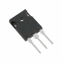
TO-247AC
Absolute Maximum Ratings
Parameter
VCES
IC @ TC = 25°C
IC @ TC = 100°C
ICM
ILM
VGE
EARV
PD @ TC = 25°C
PD @ TC = 100°C
TJ
TSTG
Collector-to-Emitter Voltage
Continuous Collector Current
Continuous Collector Current
Pulse Collector Current
Clamped Inductive Load current
�c
d
Gate-to-Emitter Voltage
Reverse Voltage Avalanche Energy
e
Maximum Power Dissipation
Maximum Power Dissipation
Operating Junction and
Storage Temperature Range
Solder Temperature Range, for 10 sec.
Max.
Units
250
104*
56
208
290
±20
1240
330
130
-55 to +150
V
A
V
mJ
W
°C
300 (0.063 in. (1.6mm) from case)
Thermal / Mechanical Characteristics
Min.
Typ.
Max.
Units
RθJC
RθCS
RθJA
Junction-to-Case- IGBT
Case-to-Sink, flat, greased surface
Junction-to-Ambient, typical socket mount
Parameter
–––
–––
–––
–––
0.24
–––
0.38
–––
40
°C/W
Wt
Weight
–––
6 (0.21)
–––
g (oz.)
*Package limited to 60A.
1
www.irf.com
07/05/04
�IRGP4050
Electrical Characteristics @ TJ = 25°C (unless otherwise specified)
Parameter
Min. Typ. Max. Units
Collector-to-Emitter Breakdown Voltage
V(BR)CES
V(BR)ECS
Emitter-to-Collector Breakdown Voltage
∆V(BR)CES/∆TJ Temperature Coeff. of Breakdown Voltage
f�
VCE(on)
Collector-to-Emitter Saturation Voltage
VGE(th)
∆VGE(th)/∆TJ
Gate Threshold Voltage
Threshold Voltage temp. coefficient
gfe
ICES
Forward Transconductance
Zero Gate Voltage Collector Current
IGES
Gate-to-Emitter Leakage Current
g�
250
18
—
—
—
—
3.0
—
34
—
—
—
—
Conditions
—
—
V VGE = 0V, IC = 250µA
—
—
V VGE = 0V, IC = 1.0A
8.2
— mV/°C VGE = 0V, IC = 1mA
IC = 30A
1.64 1.90
IC = 56A
VGE = 15V
2.04 —
V
IC = 104A, TJ = 150°C See Fig. 2, 5
2.60 —
VCE = VGE, IC = 250µA
—
6.0
-11
— mV/°C VCE = VGE, IC = 0.25mA
51
—
S VCE = 100V, IC = 56A
VGE = 0V, VCE = 250V
—
250
—
2.0
µA VGE = 0V, VCE = 10V
VGE = 0V, VCE = 250V, TJ = 150°C
— 5000
— ±100 nA VGE = ±20V
Switching Characteristics @ TJ = 25°C (unless otherwise specified)
Parameter
Qg
Qge
Qgc
td(on)
tr
td(off)
tf
Eon
Eoff
ETS
td(on)
tr
td(off)
tf
ETS
LE
Cies
Coes
Cres
Total Gate Charge (turn-on)
Gate-to-Emitter Charge (turn-on)
Gate-to-Collector Charge (turn-on)
Turn-On delay time
Rise time
Turn-Off delay time
Fall time
Turn-On Switching Loss
Turn-Off Switching Loss
Total Switching Loss
Turn-On delay time
Rise time
Turn-Off delay time
Fall time
Total Switching Loss
Internal Emitter Inductance
Input Capacitance
Output Capacitance
Reverse Transfer Capacitance
Min. Typ. Max. Units
—
—
—
—
—
—
—
—
—
—
—
—
—
—
—
—
—
—
—
230
37
78
37
35
120
59
45
125
170
35
35
130
120
280
13
4650
480
92
350
56
120
—
—
180
89
—
—
—
—
—
—
—
—
—
—
—
—
nC
ns
Conditions
IC = 56A
VCC = 200V
See Fig. 8
VGE = 15V
TJ = 25°C
IC = 30A, VCC = 180V
VGE = 15V, RG = 5.0Ω
Energy losses include "tail"
See Fig. 9, 10, 14
µJ
ns
µJ
nH
pF
TJ = 150°C
IC = 30A, VCC = 180V
VGE = 15V, RG = 5.0Ω
Energy losses include "tail"
See Fig. 11, 14
Measured 5mm from package
VGE = 0V
VCC = 30V,
See Fig. 7
f = 1.0MHz
Notes:
Repetitive rating; VGE = 20V, pulse width limited by max. junction temperature. ( See fig. 13b )
VCC = 80%(VCES ), VGE = 20V, L = 10µH, RG = 5.0Ω, (See fig. 13a).
Repetitive rating; pulse width limited by maximum junction temperature.
Pulse width ≤ 2.5ms; duty factor ≤ 0.1%.
Pulse width 5.0µs, single shot.
2
www.irf.com
�IRGP4050
140
Triangular wave:
For both:
Duty cycle : 50%
Tj = 125°C
Tsink = 90°C
Gate drive as specified
Power Dissipation = 73W
120
Clamp voltage:
80% of rated
Load Current ( A )
100
80
60
Square wave:
60% of rated
voltage
40
20
Ideal diodes
0
0.1
1
10
100
f , Frequency ( kHz )
Fig. 1 - Typical Load Current vs. Frequency
(Load Current = IRMS of fundamental)
1000
IC, Collector-to-Emitter Current (A)
IC, Collector-to-Emitter Current (A)
1000
T J = 150°C
100
10
T J = 25°C
1
V GE = 15V
20µs PULSE WIDTH
0.1
0.1
1
10
V CE, Collecto-to-Emitter Voltage (V)
Fig. 2 - Typical Output Characteristics
www.irf.com
100
100
10
T J = 150°C
1
TJ = 25°C
0.1
VCC = 50V
20µs PULSE WIDTH
0.01
0
2
4
6
8
10
12
14
16
VGE, Gate-to-Emitter Voltage (V)
Fig. 3 - Typical Transfer Characteristics
3
�IRGP4050
4.0
LIMITED BY PACKAGE
100
80
60
40
20
50
75
100
125
IC = 112A
3.0
IC = 56A
2.0
IC = 28A
0
25
VGE = 15V
80µs PULSE WIDTH
VCE , Collector-to Emitter Voltage (V)
Maximum DC Collector Current (A)
120
1.0
150
-60 -40 -20
T C , Case Temperature (°C)
0
20
40
60
80 100 120 140 160
T J , Junction Temperature (°C)
Fig. 4 - Maximum Collector Current vs. Case
Temperature
Fig. 5 - Typical Collector-to-Emitter Voltage
vs. Junction Temperature
Thermal Response ( Z thJC )
1
D = 0.50
0.1
0.20
0.10
0.05
0.01
0.001
τJ
0.02
0.01
R1
R1
τJ
τ1
τ1
R2
R2
τ2
R3
R3
τ3
τ2
τC
τ
τ3
Ri (°C/W) τi (sec)
0.0906 0.000350
0.0906 0.002209
0.2003
Ci= τi/Ri
Ci i/Ri
SINGLE PULSE
( THERMAL RESPONSE )
0.028536
Notes:
1. Duty Factor D = t1/t2
2. Peak Tj = P dm x Zthjc + Tc
0.0001
1E-006
1E-005
0.0001
0.001
0.01
0.1
1
t1 , Rectangular Pulse Duration (sec)
Fig. 6 - Maximum Effective Transient Thermal Impedance, Junction-to-Case
4
www.irf.com
�IRGP4050
100000
VGE, Gate-to-Emitter Voltage (V)
C oes = C ce + Cgc
10000
Capacitance (pF)
16
VGS = 0V,
f = 1 MHZ
C ies = C ge + C gd, C ce SHORTED
C res = C gc
Cies
1000
Coes
100
Cres
VCES = 200V
IC = 56A
14
12
10
8
6
4
2
10
0
0
50
100
150
200
0
VCE, Collector-toEmitter-Voltage(V)
7000
TJ = 25°C
I C = 56A
1800
1600
1400
1200
4000
3000
2000
1000
800
0
5
10
15
20
25
RG, Gate Resistance (Ω)
Fig. 9 - Typical Switching Losses vs. Gate
Resistance
www.irf.com
30
IC = 112A
5000
1000
0
200
�
RG = 5.0Ω
V GE = 15V
6000
Total Swiching Losses (µJ)
Total Swiching Losses (µJ)
2000
150
Fig. 8 - Typical Gate Charge vs.
Gate-to-Emitter Voltage
2400
2200
100
Q G, Total Gate Charge (nC)
Fig. 7 - Typical Capacitance vs.
Collector-to-Emitter Voltage
VCE = 200V
VGE = 15V
50
IC = 56A
IC = 28A
-55
-5
45
95
145
T J, Juntion Temperature (°C)
Fig. 10 - Typical Switching Losses vs.
Junction Temperature
5
�IRGP4050
6000
1000
Total Swiching Losses (µJ)
5000
IC, Collector-to-Emitter Current (A)
RG = 5.0Ω
TJ = 150°C
V CE= 200V
V GE = 15V
4000
3000
2000
1000
100
SAFE OPERATING AREA
10
1
0
20
40
60
80
100
IC, Collecto-to-Emitter (A)
Fig. 11 - Typical Switching Losses vs.
Collector-to-Emitter Current
6
VGE = 20V
T J = 125°
120
1
10
100
1000
VDS, Drain-to-Source Voltage (V)
Fig. 12 - Turn-Off SOA
www.irf.com
�IRGP4050
L
D.U.T.
VC *
50V
RL =
0 - 480V
1000V
c
480V
4 X I C@25°C
480µF
960V
d
* Driver same type as D.U.T.; Vc = 80% of Vce(max)
* Note: Due to the 50V power supply, pulse width and inductor
will increase to obtain rated Id.
Fig. 13a - Clamped Inductive
Fig. 13b - Pulsed Collector
Load Test Circuit
Current Test Circuit
IC
L
Driver*
D.U.T.
VC
Test Circuit
50V
1000V
c�
Fig. 14a - Switching Loss
d
e
* Driver same type
as D.U.T., VC = 480V
c
d
90%
e
VC
10%
90%
Fig. 14b - Switching Loss
t d(off)
10%
I C 5%
Waveforms
tf
tr
t d(on)
t=5µs
E on
E off
E ts = (Eon +Eoff )
www.irf.com
7
�IRGP4050
TO-247AC Package Outline
Dimensions are shown in millimeters (inches)
TO-247AC Part Marking Information
(;$03/(� 7+,6�,6�$1�,5)3(���
:,7+�$66(0%/