PD - 9.770A
IRGPF40F
INSULATED GATE BIPOLAR TRANSISTOR
Features
Fast Speed IGBT
C
• Switching-loss rating includes all "tail" losses
• Optimized for medium operating frequency (1 to
10kHz) See Fig. 1 for Current vs. Frequency
curve
VCES = 900V
VCE(sat) ≤ 3.3V
G
@VGE = 15V, I C = 17A
E
n-channel
Description
Insulated Gate Bipolar Transistors (IGBTs) from International Rectifier have
higher usable current densities than comparable bipolar transistors, while at
the same time having simpler gate-drive requirements of the familiar power
MOSFET. They provide substantial benefits to a host of high-voltage, highcurrent applications.
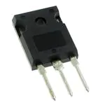
TO-247AC
Absolute Maximum Ratings
Parameter
VCES
IC @ T C = 25°C
IC @ T C = 100°C
ICM
ILM
VGE
EARV
PD @ T C = 25°C
PD @ T C = 100°C
TJ
TSTG
Collector-to-Emitter Voltage
Continuous Collector Current
Continuous Collector Current
Pulsed Collector Current
Clamped Inductive Load Current
Gate-to-Emitter Voltage
Reverse Voltage Avalanche Energy
Maximum Power Dissipation
Maximum Power Dissipation
Operating Junction and
Storage Temperature Range
Soldering Temperature, for 10 sec.
Mounting torque, 6-32 or M3 screw.
Max.
Units
900
31
17
62
62
±20
15
160
65
-55 to +150
V
A
V
mJ
W
°C
300 (0.063 in. (1.6mm) from case)
10 lbf•in (1.1N•m)
Thermal Resistance
Parameter
RθJC
RθCS
RθJA
Wt
Junction-to-Case
Case-to-Sink, flat, greased surface
Junction-to-Ambient, typical socket mount
Weight
C-261
Min.
Typ.
Max.
—
—
—
—
—
0.24
—
6 (0.21)
0.77
—
40
—
Units
°C/W
g (oz)
Revision 0
�IRGPF40F
Electrical Characteristics @ TJ = 25°C (unless otherwise specified)
VCE(on)
Parameter
Collector-to-Emitter Breakdown Voltage
Emitter-to-Collector Breakdown Voltage
Temperature Coeff. of Breakdown Voltage
Collector-to-Emitter Saturation Voltage
VGE(th)
∆VGE(th)/∆TJ
gfe
ICES
Gate Threshold Voltage
Temperature Coeff. of Threshold Voltage
Forward Transconductance
Zero Gate Voltage Collector Current
IGES
Gate-to-Emitter Leakage Current
V(BR)CES
V(BR)ECS
∆V(BR)CES/∆TJ
Min. Typ. Max. Units
Conditions
900
—
—
V
VGE = 0V, I C = 250µA
20
—
—
V
VGE = 0V, IC = 1.0A
— 0.80 —
V/°C VGE = 0V, I C = 1.0mA
—
2.5
3.3
IC = 17A
V GE = 15V
—
3.2
—
V
IC = 31A
See Fig. 2, 5
—
2.9
—
IC = 17A, T J = 150°C
3.0
—
5.5
VCE = VGE, IC = 250µA
—
-12
— mV/°C VCE = VGE, IC = 250µA
5.2
13
—
S
VCE = 100V, I C = 17A
—
—
250
µA
VGE = 0V, V CE = 900V
—
— 1000
VGE = 0V, V CE = 900V, T J = 150°C
—
— ±100 nA
VGE = ±20V
Switching Characteristics @ TJ = 25°C (unless otherwise specified)
Parameter
Total Gate Charge (turn-on)
Gate - Emitter Charge (turn-on)
Gate - Collector Charge (turn-on)
Turn-On Delay Time
Rise Time
Turn-Off Delay Time
Fall Time
Turn-On Switching Loss
Turn-Off Switching Loss
Total Switching Loss
Turn-On Delay Time
Rise Time
Turn-Off Delay Time
Fall Time
Total Switching Loss
Internal Emitter Inductance
Input Capacitance
Output Capacitance
Reverse Transfer Capacitance
Qg
Qge
Qgc
td(on)
tr
td(off)
tf
Eon
Eoff
Ets
td(on)
tr
td(off)
tf
Ets
LE
Cies
Coes
Cres
Min.
—
—
—
—
—
—
—
—
—
—
—
—
—
—
—
—
—
—
—
Typ. Max. Units
Conditions
45
68
IC = 17A
8.7
13
nC
VCC = 400V
See Fig. 8
15
23
VGE = 15V
28
—
TJ = 25°C
12
—
ns
IC = 17A, V CC = 720V
170 320
VGE = 15V, R G = 10Ω
110 300
Energy losses include "tail"
0.52 —
1.05 —
mJ
See Fig. 9, 10, 11, 14
1.57 3.1
27
—
TJ = 150°C,
14
—
ns
IC = 17A, V CC = 720V
250
—
VGE = 15V, R G = 10Ω
240
—
Energy losses include "tail"
3.0
—
mJ
See Fig. 10, 14
13
—
nH
Measured 5mm from package
1200 —
VGE = 0V
91
—
pF
VCC = 30V
See Fig. 7
15
—
ƒ = 1.0MHz
Notes:
Repetitive rating; V GE=20V, pulse width
limited by max. junction temperature.
( See fig. 13b )
Repetitive rating; pulse width limited
by maximum junction temperature.
VCC=80%(V CES), VGE=20V, L=10µH,
R G= 10Ω, ( See fig. 13a )
Pulse width ≤ 80µs; duty factor ≤ 0.1%.
C-262
Pulse width 5.0µs,
single shot.
�IRGPF40F
50
For b oth :
40
LO A D CU R R E N T (A )
Triangula r w ave:
D uty c y cle: 50%
TJ = 125°C
T sink = 90° C
G ate driv e as spe c ified
P o w e r Diss ipa tio n = 3 5W
C lamp voltage:
80% of rated
30
S quare w ave:
60% of rated
voltage
20
10
Ideal diodes
0
0.1
1
10
100
f, F re quency (kH z)
Fig. 1 - Typical Load Current vs. Frequency
(For square wave, I=I RMS of fundamental; for triangular wave, I=I PK)
1000
IC , Collector-to-Em itter C urrent (A )
I C , C ollector-to-E mitter C urrent (A )
1000
100
TJ = 2 5°C
TJ = 1 50 °C
10
V G E = 15 V
20 µs P UL S E W ID TH
1
1
T J = 25 °C
100
TJ = 1 50 °C
10
V C C = 1 00 V
5 µ s P U L S E W ID TH
1
5
10
10
15
V G E , G ate -to-E m itter V olta ge (V )
V C E , C o llector-to-Em itter V oltage (V)
Fig. 3 - Typical Transfer Characteristics
Fig. 2 - Typical Output Characteristics
C-263
20
�IRGPF40F
5.0
V G E = 15 V
V C E , C o llec to r-to-E m itter V oltage (V )
M axim um D C C ollector C urrent (A)
40
30
20
10
V G E = 1 5V
8 0µ s P U LS E W IDTH
I C = 3 4A
4.0
3.0
I C = 1 7A
I C = 8.5 A
2.0
0
25
50
75
100
125
-60
150
T C , C ase Tem perature (°C )
-40
-20
0
20
40
60
80
100 120 140 160
T C , C a s e Te m p e ra ture (°C )
Fig. 5 - Collector-to-Emitter Voltage vs.
Case Temperature
Fig. 4 - Maximum Collector Current vs.
Case Temperature
T herm al Response (Z th JC )
1
D = 0 .5 0
0.2 0
0.1
0.1 0
PD M
0 .05
0.0 2
t
t2
N o te s:
1 . D u ty fa c to r D = t
0.0 1
0.01
0.00001
1
SIN G LE P UL SE
(TH ER MA L R E SP O NS E )
1
/ t
2
2 . P e a k TJ = P D M x Z thJ C + T C
0.0001
0.001
0.01
0.1
1
t 1 , R ectangular Pulse D uration (sec)
Fig. 6 - Maximum Effective Transient Thermal Impedance, Junction-to-Case
C-264
10
�IRGPF40F
24 0 0
V G E , G ate-to-E m itter V oltag e (V )
20 0 0
C, C apacitance (pF)
20
V GE = 0V,
f = 1MHz
C ies = C ge + C gc , Cce SHORTED
C res = C gc
C oes = C ce + C gc
16
16 0 0
Cies
12
12 0 0
Coes
800
400
V C E = 40 0V
I C = 17 A
Cres
0
8
4
0
1
10
100
0
10
V C E , C o llector-to-Em itter V oltage (V)
Fig. 7 - Typical Capacitance vs.
Collector-to-Emitter Voltage
VC C
VG E
TC
IC
T o tal S w itc hin g L os se s (m J)
1 .7 4
1 .6 6
1 .6 2
50
I C = 34 A
I C = 17 A
1
I C = 8.5 A
1 .5 8
1 .5 4
0.1
10
40
10
= 72 0V
= 1 5V
= 25°C
= 17 A
1 .7 0
0
30
Fig. 8 - Typical Gate Charge vs.
Gate-to-Emitter Voltage
To ta l S w itc hing Lo sse s (m J)
1 .7 8
20
Q g , T o tal G a te C h a rg e (n C )
20
30
40
50
60
R G = 10 Ω
V GE = 15 V
V CC = 7 20 V
-60
R G , G a te R e s is ta n c e ( Ω )
-40
-20
0
20
40
60
80
100 120 140 160
TC , C a s e T e m p era tu re (°C )
W
Fig. 9 - Typical Switching Losses vs. Gate
Resistance
Fig. 10 - Typical Switching Losses vs.
Case Temperature
C-265
�IRGPF40F
RG
TC
VCC
VGE
8
1000
= 10 Ω
= 1 50°C
= 72 0V
= 1 5V
I C , C ollec to r-to-E m itte r C urren t (A )
T ota l S w itc h ing L o s s e s (m J )
10
6
4
2
0
VGGE E= 20 V
T J = 12 5°C
100
S A FE O P E R A TIN G A R E A
10
1
0.1
0
10
20
30
40
1
10
100
V C E , C o lle cto r-to-E m itte r V olta g e (V )
I C , C o lle c to r-to -E m itte r C u rre n t (A )
Fig. 11 - Typical Switching Losses vs.
Collector-to-Emitter Current
Fig. 12 - Turn-Off SOA
Refer to Section D for the following:
Appendix F: Section D - page D-8
Fig. 13a - Clamped Inductive Load Test Circuit
Fig. 13b - Pulsed Collector Current Test Circuit
Fig. 14a - Switching Loss Test Circuit
Fig. 14b - Switching Loss Waveform
Package Outline 3 - JEDEC Outline TO-247AC (TO-3P)
C-266
Section D - page D-13
1000
�Note: For the most current drawings please refer to the IR website at:
http://www.irf.com/package/
�