IRGS4045DPbF
INSULATED GATE BIPOLAR TRANSISTOR WITH
ULTRAFAST SOFT RECOVERY DIODE
VCES = 600V
C
IC 6.0A, TC = 100°C
tsc > 5µs, Tjmax = 175°C
C
E
G
VCE(on) typ. 1.7V
G
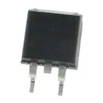
D2-Pak
IRGS4045DPbF
E
n-channel
Applications
Appliance Motor Drive
Inverters
SMPS
G
Gate
Low VCE(ON) and switching losses
Square RBSOA and maximum junction temperature 175°C
Positive V CE(ON) temperature coefficient and tighter
distribution of parameters
5μs short circuit SOA
Ultra fast soft recovery copak diode
Lead-free, RoHS compliant
IRGS4045DPbF
E
Emitter
Features
Base part number
C
Colletor
Package Type
Benefits
High efficiency in a wide range of applications and
switching frequencies
Improved reliability due to rugged hard switching performance
and higher power capability
Excellent current sharing in parallel operation
Enables short circuit protection scheme
Performance optimized for motor drive operation
Environmentally friendly
Standard Pack
Form
Tube
Tape and Reel Left
Tape and Reel Right
D2Pak
Orderable Part Number
Quantity
50
800
800
IRGS4045DPbF
IRGS4045DTRLPbF
IRGS4045DTRRPbF
Absolute Maximum Ratings
VCES
I C@ TC = 25°C
I C@ TC = 100°C
I CM
I LM
I F@TC=25°C
I F@TC=100°C
I FM
VGE
PD @ TC =25°
PD @ TC =100°
TJ
TSTG
Parameter
Collector-to-Emitter Breakdown Voltage
Continuous Collector Current
Continuous Collector Current
Pulsed Collector Current, VGE = 15V
Clamped Inductive Load Current, VGE = 20V
Diode Continuous Forward Current
Diode Continuous Forward Current
Diode Maximum Forward Current
Continuous Gate-to-Emitter Voltage
Transient Gate-to-Emitter Voltage
Maximum Power Dissipation
Maximum Power Dissipation
Operating Junction and
Storage Temperature Range
Soldering Temperature, for 10 seconds
Max.
600
12
6.0
18
24
8.0
4.0
24
± 20
± 30
77
39
c
d
Units
V
A
V
W
°C
-55 to + 175
300 (0.063 in. (1.6mm) from case)
Thermal Resistance
RJC
RJC
RCS
RJA
Parameter
Junction-to-Case - IGBT
Junction-to-Case - Diode
e
e
Case-to-Sink, Flat, Greased Surface
Junction-to-Ambient (PCB Mountet, steady-state)
g
Min.
–––
–––
–––
–––
Typ.
–––
–––
0.5
–––
Max.
1.9
6.3
–––
40
Units
°C/W
*Qualification standards can be found at http://www.irf.com/
1
www.irf.com © 2012 International Rectifier
October 10, 2012
�IRGS4045DPbF
Electrical Characteristics @ TJ = 25°C (unless otherwise specified)
Min.
Typ.
Max.
Units
V(BR)CES
V(BR)CES/TJ
Collector-to-Emitter Breakdown Voltage
Temperature Coeff. of Breakdown Voltage
Parameter
600
—
—
—
0.36
1.7
—
—
2.0
V
V/°C
VCE(on)
Collector-to-Emitter Saturation Voltage
Gate Threshold Voltage
Threshold Voltage temp. coefficient
Forward Transconductance
2.07
2.14
—
-13
5.8
—
—
—
6.5
—
—
25
V
VGE(th)
VGE(th) /TJ
gfe
ICES
—
—
4.0
—
—
—
—
—
—
1.60
250
2.30
—
—
1.30
—
—
±100
VFM
Collector-to-Emitter Leakage Current
Diode Forward Voltage Drop
Gate-to-Emitter Leakage Current
IGES
Switching Characteristics @ TJ = 25°C (unless otherwise specified)
Parameter
Min.
Typ.
h
Max.
V
nA
—
—
—
13
3.1
6.4
19.5
4.65
9.6
Eon
Eoff
Etotal
td(on)
tr
td(off)
tf
Turn-On Switching Loss
Turn-Off Switching Loss
Total Switching Loss
Turn-On delay time
Rise time
Turn-Off delay time
Fall time
—
—
—
—
—
—
—
56
122
178
27
11
75
17
86
143
229
35
15
93
22
Eon
Eoff
Etotal
td(on)
tr
td(off)
tf
Cies
Turn-On Switching Loss
Turn-Off Switching Loss
Total Switching Loss
Turn-On delay time
Rise time
Turn-Off delay time
Fall time
Input Capacitance
—
—
—
—
—
—
—
—
140
189
329
26
12
95
32
350
—
—
—
—
—
—
—
—
Coes
Cres
Output Capacitance
Reverse Transfer Capacitance
—
—
29
10
—
—
pF
RBSOA
Reverse Bias Safe Operating Area
FULL SQUARE
SCSOA
Short Circuit Safe Operating Area
5
—
—
μs
Erec
Reverse recovery energy of the diode
Diode Reverse recovery time
Peak Reverse Recovery Current
—
178
74
12
—
μJ
ns
A
—
—
f
IC = 6.0A, VGE = 15V, TJ = 150°C
IC = 6.0A, VGE = 15V, TJ = 175°C
VCE = VGE, IC = 150μA
IF = 6.0A
IF = 6.0A, TJ = 175°C
VGE = ± 20 V
Conditions
Units
Total Gate Charge (turn-on)
Gate-to-Emitter Charge (turn-on)
Gate-to-Collector Charge (turn-on)
—
—
f
VGE = 0V, Ic = 250μA ( 25 -175 oC )
IC = 6.0A, VGE = 15V, TJ = 25°C
V
o
mV/°C VCE = VGE, IC = 250μA ( 25 -175 C )
VCE = 25V, IC = 6.0A, PW =80 s
S
VGE = 0V,VCE = 600V
μA
VGE = 0V, VCE = 600V, TJ =175°C
Qg
Qge
Qgc
trr
Irr
Conditions
VGE = 0V, Ic =100 μA
nC
μJ
IC = 6.0A
VCC = 400V
VGE = 15V
IC = 6.0A, VCC = 400V, VGE = 15V
RG = 47, L=1mH, LS= 150nH, TJ = 25°C
E nergy los s es include tail and diode revers e recovery
ns
μJ
IC = 6.0A, VCC = 400V
RG = 47, L=1mH, LS= 150nH
TJ = 25°C
IC = 6.0A, VCC = 400V, VGE = 15V
RG = 47, L=1mH, LS= 150nH, TJ = 175°C
E nergy los s es include tail and diode revers e recovery
ns
IC = 6.0A, VCC = 400V
RG = 47, L=1mH, LS= 150nH
TJ = 175°C
VGE = 0V
VCC = 30V
f = 1Mhz
TJ = 175°C, IC = 24A
VCC = 500V, Vp =600V
RG = 100, VGE = +20V to 0V
VCC = 400V, Vp =600V
RG = 100, VGE = +15V to 0V
TJ = 175oC
VCC = 400V, IF = 6.0A
VGE = 15V, Rg = 47, L=1mH, LS=150nH
Notes:
VCC = 80% (VCES), VGE = 15V, L = 1.0mH, RG = 47
Pulse width limited by max. junction temperature.
R is measured at T J approximately 90°C.
Refer to AN-1086 for guidelines for measuring V(BR)CES safely.
When mounted on 1" square PCB (FR-4 or G-10 Material). For recommended footprint and soldering techniques refer to application note #AN-994.
Maximum limits are based on statistical sample size characterization.
2
www.irf.com © 2012 International Rectifier
October 10, 2012
�IRGS4045DPbF
14
80
12
70
60
50
8
Ptot (W)
IC (A)
10
6
40
30
4
20
2
10
0
0
0
20
40
60
80 100 120 140 160 180
0
20
40
60
80 100 120 140 160 180
T C (°C)
T C (°C)
Fig. 1 - Maximum DC Collector Current vs.
Case Temperature
Fig. 2 - Power Dissipation vs. Case
Temperature
100
100
10μsec
10
10
IC A)
IC (A)
100μsec
DC
1
1
Tc = 25°C
Tj = 175°C
Single Pulse
0
0.1
1
10
100
10
1000
100
VCE (V)
VCE (V)
Fig. 3 - Forward SOA,
TC = 25°C, TJ 175°C, VGE = 15V
Fig. 4 - Reverse Bias SOA
TJ = 175°C, VGE = 20V
20
20
Top
V
= 18V
GE
V
= 15V
GE
VGE = 12V
15
V
= 10V
GE
Bottom VGE = 8.0V
10
ICE (A)
ICE (A)
15
Top
Bottom
10
V
= 18V
GE
V
= 15V
GE
V
= 12V
GE
V
= 10V
GE
V
= 8.0V
GE
5
5
0
0
0
3
1000
2
4
6
8
10
0
2
4
6
8
10
VCE (V)
VCE (V)
Fig. 5 - Typ. IGBT Output Characteristics
TJ = -40°C; tp = 80μs
Fig. 6 - Typ. IGBT Output Characteristics
TJ = 25°C; tp = 80μs
www.irf.com © 2012 International Rectifier
October 10, 2012
�IRGS4045DPbF
20
Top
Bottom
18
16
-40°C
25°C
175°C
14
12
IF (A)
ICE (A)
15
20
V
= 18V
GE
V
= 15V
GE
V
= 12V
GE
V
= 10V
GE
V
= 8.0V
GE
10
10
8
6
5
4
2
0
0
0
2
4
6
8
10
0.0
1.0
2.0
VCE (V)
Fig. 8 - Typ. Diode Forward Characteristics
tp = 80μs
10
10
8
8
ICE = 3.0A
VCE (V)
VCE (V)
Fig. 7 - Typ. IGBT Output Characteristics
TJ = 175°C; tp = 80μs
6
ICE = 6.0A
ICE = 12A
4
2
6
ICE = 3.0A
ICE = 6.0A
ICE = 12A
4
2
0
0
5
10
15
20
5
10
VGE (V)
20
Fig. 10 - Typical VCE vs. VGE
TJ = 25°C
20
IC, Collector-to-Emitter Current (A)
10
8
VCE (V)
15
VGE (V)
Fig. 9 - Typical VCE vs. VGE
TJ = -40°C
ICE = 3.0A
ICE = 6.0A
6
ICE = 12A
4
2
18
T J = 25°C
T J = 175°C
16
14
12
10
8
6
4
2
0
0
5
10
15
20
VGE (V)
Fig. 11 - Typical VCE vs. VGE
TJ = 175°C
4
3.0
VF (V)
www.irf.com © 2012 International Rectifier
4
6
8
10
12
14
16
VGE, Gate-to-Emitter Voltage (V)
Fig. 12 - Typ. Transfer Characteristics
VCE = 50V; tp = 10μs
October 10, 2012
�IRGS4045DPbF
400
1000
350
Swiching Time (ns)
Energy (μJ)
300
250
200
EOFF
150
tdOFF
100
tF
tdON
10
tR
EON
100
50
1
0
2
4
6
8
10
12
14
2
4
8
10
12
14
IC (A)
IC (A)
Fig. 13 - Typ. Energy Loss vs. IC
TJ = 175°C; L = 1mH; VCE = 400V, RG = 47; VGE = 15V.
Fig. 14 - Typ. Switching Time vs. IC
TJ = 175°C; L=1mH; VCE= 400V
RG= 47; VGE= 15V
220
1000
200
EOFF
Swiching Time (ns)
180
Energy (μJ)
6
160
EON
140
120
tdOFF
100
tF
tdON
10
tR
100
80
60
1
0
25
50
75
100
125
0
25
100
125
Fig. 16- Typ. Switching Time vs. RG
TJ = 175°C; L=1mH; VCE= 400V
ICE= 6.0A; VGE= 15V
Fig. 15 - Typ. Energy Loss vs. RG
TJ = 175°C; L = 1mH; VCE = 400V, ICE = 6.0A; VGE = 15V
22
30
20
25
RG = 10
18
20
16
15
IRR (A)
IRR (A)
75
RG ()
Rg ()
RG = 22
10
RG = 47
5
RG = 100
14
12
10
8
6
0
2
4
6
8
10
12
14
IF (A)
Fig. 17 - Typical Diode IRR vs. IF
TJ = 175°C
5
50
www.irf.com © 2012 International Rectifier
0
25
50
75
100
125
RG (
Fig. 18 - Typical Diode IRR vs. RG
TJ = 175°C; IF = 6.0A
October 10, 2012
�IRGS4045DPbF
1200
20
18
1000
12A
10
QRR (nC)
IRR (A)
16
14
12
22
800
47
6.0A
600
10
100
400
3.0A
8
200
6
0
200
400
600
800
1000
0
1200
500
diF /dt (A/μs)
1500
Fig. 20 - Typical Diode QRR
VCC= 400V; VGE= 15V; TJ = 175°C
Fig. 19- Typical Diode IRR vs. diF/dt
VCC= 400V; VGE= 15V;
ICE= 6.0A; TJ = 175°C
350
50
20
300
40
Time (μs)
RG = 47
10
30
5
20
Current (A)
Isc
RG = 22
200
Tsc
15
RG = 10
250
Energy (μJ)
1000
diF /dt (A/μs)
150
RG = 100
100
50
10
0
2
4
6
8
10
12
14
8
10
12
IF (A)
18
Fig. 22- Typ. VGE vs. Short Circuit Time
VCC=400V, TC =25°C
1000
16
VGE, Gate-to-Emitter Voltage (V)
Cies
Capacitance (pF)
16
VGE (V)
Fig. 21 - Typical Diode ERR vs. IF
TJ = 175°C
100
Coes
10
Cres
1
V CES = 400V
14
V CES = 300V
12
10
8
6
4
2
0
0
100
200
300
400
500
VCE (V)
Fig. 23- Typ. Capacitance vs. VCE
VGE= 0V; f = 1MHz
6
14
www.irf.com © 2012 International Rectifier
0
2
4
6
8
10
12
14
Q G, Total Gate Charge (nC)
Fig. 24 - Typical Gate Charge vs. VGE
ICE = 6.0A, L=600μH
October 10, 2012
�IRGS4045DPbF
Thermal Response ( Z thJC )
10
1
D = 0.50
0.20
0.10
0.05
0.1
J
0.02
0.01
R1
R1
J
1
R3
R3
Ri (°C/W) i (sec)
R4
R4
C
2
1
2
3
3
4
4
Ci= iRi
Ci iRi
SINGLE PULSE
( THERMAL RESPONSE )
0.01
R2
R2
0.0301
0.000004
0.7200
0.000067
0.7005
0.000898
0.4479
0.005416
Notes:
1. Duty Factor D = t1/t2
2. Peak Tj = P dm x Zthjc + Tc
0.001
1E-006
1E-005
0.0001
0.001
0.01
0.1
t1 , Rectangular Pulse Duration (sec)
Fig 25. Maximum Transient Thermal Impedance, Junction-to-Case (IGBT)
10
Thermal Response ( Z thJC )
D = 0.50
0.20
1
0.10
0.05
J
0.02
0.1
0.01
R1
R1
J
1
R2
R2
R3
R3
C
2
1
2
3
3
Ci= iRi
Ci iRi
SINGLE PULSE
( THERMAL RESPONSE )
0.01
1E-006
1E-005
0.0001
Ri (°C/W) i (sec)
R4
R4
4
4
0.2056
0.000019
1.4132
0.000095
3.3583
0.001204
1.8245
0.009127
Notes:
1. Duty Factor D = t1/t2
2. Peak Tj = P dm x Zthjc + Tc
0.001
0.01
0.1
1
t1 , Rectangular Pulse Duration (sec)
Fig. 26. Maximum Transient Thermal Impedance, Junction-to-Case (DIODE)
7
www.irf.com © 2012 International Rectifier
October 10, 2012
�IRGS4045DPbF
L
L
DUT
0
VCC
1K
Fig.C.T.1 - Gate Charge Circuit (turn-off)
Fig.C.T.3 - S.C.SOA Circuit
Fig.C.T.5 - Resistive Load Circuit
8
www.irf.com © 2012 International Rectifier
80 V
+
-
DUT
Rg
480V
Fig.C.T.2 - RBSOA Circuit
Fig.C.T.4 - Switching Loss Circuit
Fig.C.T.6 - Typical Filter Circuit for
V(BR)CES Measurement
October 10, 2012
�IRGS4045DPbF
600
12
600
500
10
500
400
8
400
6
300
30
25
tr
TEST
CURRENT
90% ICE
200
4
5% ICE
100
VCE (V)
VCE (V)
tf
300
90% test
current
2
100
0
0
-2
-100
10
10% test
current
0
0.2
0.4
0.6
0.8
0
Fig. WF1 - Typ. Turn-off Loss Waveform
@ TJ = 175°C using Fig. CT.4
100
t RR
-5
-400
-10
-500
-15
-20
0.05
0.15
0.25
time (µS)
WF.3- Typ. Diode Recovery Waveform
@ TJ = 175°C using CT.4
9
www.irf.com © 2012 International Rectifier
Vce (V)
VF (V)
10%
Peak
IRR
Peak
IRR
-600
-0.05
450
5
0
80
500
10
QRR
-200
-300
4.7
Fig. WF2 - Typ. Turn-on Loss Waveform
@ TJ = 175°C using Fig. CT.4
15
-100
4.5
-5
time (µs)
time(µs)
0
Eon Loss
4.3
1
5
5% VCE
Eoff Loss
-100
-0.2
15
200
5% VCE
0
20
VCE
70
400
60
350
50
300
40
250
200
30
ICE
20
150
10
100
0
50
-10
0
-20
-2 -1 0 1 2 3 4 5 6 7 8
Time (uS)
WF.4- Typ. Short Circuit Waveform
@ TJ = 25°C using CT.3
October 10, 2012
�IRGS4045DPbF
D2Pak Package Outline
Dimensions are shown in millimeters (inches)
D2Pak Part Marking Information
7+,6�,6�$1�,5)���6�:,7+
/27�&2'(�����
$66(0%/('�21�::���������
,1�7+(�$66(0%/