IRGS4640DPbF
IRGSL4640DPbF
IRGB4640DPbF
IRGP4640D(-E)PbF
Insulated Gate Bipolar Transistor with Ultrafast Soft Recovery Diode
VCES = 600V
C
IC = 40A, TC =100°C
tSC ≥ 5µs, TJ(max) = 175°C
G
C
G
E
VCE(ON) typ. = 1.60V @ IC = 24A
n-channel
Applications
• Industrial Motor Drive
• Inverters
• UPS
• Welding
G
Gate
E
E
C
G
IRGS4640DPbF
D2Pak
IRGSL4640DPbF
TO-262Pak
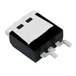
IRGB4640DPbF
TO-220AC
C
G
E
C
G
E
IRGP4640DPbF IRGP4640D-EPbF
TO-247AD
TO-247AC
C
Collector
Features
E
Emitter
Benefits
Low VCE(ON) and switching losses
High efficiency in a wide range of applications and switching
Square RBSOA and maximum junction temperature 175°C
Positive VCE (ON) temperature coefficient
5µs Short Circuit SOA
Lead-Free, RoHS Compliant
Base part number
E
C
G
Package Type
2
IRGS4640DPbF
D Pak
IRGSL4640DPbF
IRGB4640DPbF
IRGP4640DPbF
IRGP4640D-EPbF
TO-262
TO-220AB
TO-247AC
TO-247AD
Improved reliability due to rugged hard switching
performance and high power capability
Excellent current sharing in parallel operation
Enables short circuit protection scheme
Environmentally friendly
Standard Pack
Form
Quantity
Tube
50
Tape and Reel Right
800
Tape and Reel Left
800
Tube
50
Tube
50
Tube
25
Tube
25
Orderable Part Number
IRGS4640DPbF
IRGS4640DTRRPbF
IRGS4640DTRLPbF
IRGSL4640DPbF
IRGB4640DPbF
IRGP4640DPbF
IRGP4640D-EPbF
Absolute Maximum Ratings
VCES
IC @ TC = 25°C
IC @ TC = 100°C
ICM
ILM
IF @ TC = 25°C
IF @ TC = 100°C
IFM
VGE
PD @ TC = 25°C
PD @ TC = 100°C
TJ
TSTG
Parameter
Max.
Units
Collector-to-Emitter Voltage
Continuous Collector Current
Continuous Collector Current
Pulse Collector Current, VGE = 15V
Clamped Inductive Load Current, VGE = 20V
Diode Continuous Forward Current
Diode Continuous Forward Current
Diode Maximum Forward Current
Continuous Gate-to-Emitter Voltage
Transient Gate to Emitter Voltage
Maximum Power Dissipation
Maximum Power Dissipation
Operating Junction and
Storage Temperature Range
Soldering Temperature, for 10 sec. (1.6mm from case)
Mounting Torque, 6-32 or M3 Screw (TO-220, TO-247)
600
65
40
72
96
65
40
96
±20
±30
250
125
-55 to +175
V
A
V
W
300
10 lbf·in (1.1 N·m)
C
Notes through are on page 8
1
www.irf.com
© 2015 International Rectifier
Submit Datasheet Feedback
January 20, 2015
�IRGS/SL/B/P4640D/EPbF
Thermal Resistance
RθJC (IGBT)
Parameter
Thermal Resistance Junction-to-Case (D2Pak, TO-220, TO-262)
Min.
–––
Typ.
–––
Max. Units
0.60
Thermal Resistance Junction-to-Case (TO-247)
–––
–––
0.60
–––
–––
1.53
–––
–––
1.62
Thermal Resistance, Case-to-Sink (flat, greased surface– TO 220, D Pak, TO-262)
–––
0.50
–––
Thermal Resistance, Case-to-Sink (flat, greased surface– TO 247)
–––
0.24
–––
Thermal Resistance, Junction-to-Ambient (PCB Mount - D Pak, TO-262)
–––
–––
40
Thermal Resistance, Junction-to-Ambient (Socket Mount –TO-247)
–––
–––
40
Thermal Resistance, Junction-to-Ambient (Socket Mount –TO-220)
–––
–––
62
2
RθJC (Diode)
Thermal Resistance Junction-to-Case (D Pak, TO-220, TO-262)
Thermal Resistance Junction-to-Case (TO-247)
2
RθCS
2
RθJA
Electrical Characteristics @ TJ = 25°C (unless otherwise specified)
Parameter
Min.
Typ.
V(BR)CES
Collector-to-Emitter Breakdown Voltage
ΔV(BR)CES/ΔTJ Temperature Coeff. of Breakdown Voltage
VCE(on)
Collector-to-Emitter Saturation Voltage
Max.
Units
600
—
—
V
—
0.30
—
—
1.60
1.90
—
1.90
—
—
2.0
—
IC = 24A, VGE = 15V, TJ = 25°C
V
4.0
—
6.5
ΔVGE(th)/ΔTJ
Threshold Voltage Temp. Coefficient
—
-18
—
gfe
Forward Transconductance
—
17
—
S
—
2.0
25
µA
ICES
Collector-to-Emitter Leakage Current
—
775
—
IGES
Gate-to-Emitter Leakage Current
VFM
Diode Forward Voltage Drop
—
—
—
1.8
±100
2.6
—
1.28
—
© 2015 International Rectifier
IC = 24A, VGE = 15V, TJ = 150°C
IC = 24A, VGE = 15V, TJ = 175°C
Gate Threshold Voltage
www.irf.com
Conditions
VGE = 0V, IC = 100µA
V/°C VGE = 0V, IC = 1mA (25°C-175°C)
VGE(th)
2
°C/W
V
VCE = VGE, IC = 700µA
mV/°C VCE = VGE, IC = 1.0mA (25°C-175°C)
VCE = 50V, IC = 24A, PW = 80µs
VGE = 0V, VCE = 600V
VGE = 0V, VCE = 600V, TJ = 175°C
nA
V
VGE = ±20V
IF = 24A
IF = 24A, TJ = 175°C
Submit Datasheet Feedback
January 20, 2015
�IRGS/SL/B/P4640D/EPbF
Switching Characteristics @ TJ = 25°C (unless otherwise specified)
Parameter
Min.
Typ.
Total Gate Charge
—
50
Qg
Gate-to-Emitter Charge
—
13
Qge
Qgc
Gate-to-Collector Charge
—
21
Eon
Turn-On Switching Loss
—
115
Eoff
Turn-Off Switching Loss
—
600
Total Switching Loss
—
715
Etotal
td(on)
Turn-On delay time
—
41
tr
Rise time
—
22
Turn-Off delay time
—
104
td(off)
tf
Fall time
—
29
Turn-On Switching Loss
—
420
Eon
Turn-Off Switching Loss
—
840
Eoff
Total Switching Loss
—
1260
Etotal
Turn-On delay time
—
40
td(on)
—
—
—
—
—
—
nC
µJ
IC = 24A
VGE = 15V
VCC = 400V
IC = 24A, VCC = 400V, VGE=15V
RG = 10Ω, L = 200µH, LS = 150nH,
TJ = 25°C
Energy losses include tail & diode
reverse recovery
µJ
IC = 24A, VCC = 400V, VGE=15V
RG = 10Ω, L = 200µH, LS = 150nH,
TJ = 175°C
ns
Energy losses include tail & diode
reverse recovery
RBSOA
Reverse Bias Safe Operating Area
SCSOA
Short Circuit Safe Operating Area
5.0
—
—
µs
Erec
trr
Irr
Reverse Recovery Energy of the Diode
Diode Reverse Recovery Time
Peak Reverse Recovery Current
—
—
—
621
89
37
—
—
—
µJ
ns
A
© 2015 International Rectifier
Conditions
ns
Rise time
Turn-Off delay time
Fall time
Input Capacitance
Output Capacitance
Reverse Transfer Capacitance
www.irf.com
24
125
39
1490
129
45
Units
tr
td(off)
tf
Cies
Coes
Cres
3
—
—
—
—
—
—
Max
75
20
31
201
700
901
53
31
115
41
—
—
—
—
pF
FULL SQUARE
VGE = 0V
VCC = 30V
f = 1.0MHz
TJ = 175°C, IC = 96A
VCC = 480V, Vp ≤ 600V
RG = 10Ω, VGE = +20V to 0V
VCC = 400V, Vp ≤ 600V
RG = 10Ω, VGE = +15V to 0V
TJ = 175°C
VCC = 400V, IF = 24A, VGE = 15V,
Rg = 10Ω, L = 200µH, LS = 150nH
Submit Datasheet Feedback
January 20, 2015
�IRGS/SL/B/P4640D/EPbF
70
300
60
250
50
200
Ptot (W)
IC (A)
40
30
150
100
20
50
10
0
0
25
50
75
100
125
150
175
25
50
75
100
125
150
175
T C (°C)
T C (°C)
Fig. 2 - Power Dissipation vs.
Case Temperature
Fig. 1 - Maximum DC Collector Current vs.
Case Temperature
1000
1000
100
100
IC (A)
IC (A)
10µsec
10
100µsec
1
10
1msec
Tc = 25°C
Tj = 175°C
Single Pulse
DC
1
0.1
1
10
100
1000
10
10000
100
VCE (V)
VCE (V)
Fig. 4 - Reverse Bias SOA
TJ = 175°C; VGE = 20V
Fig. 3 - Forward SOA
TC = 25°C; TJ ≤ 175°C; VGE = 15V
90
90
80
80
VGE = 18V
VGE = 15V
VGE = 12V
VGE = 10V
VGE = 8.0V
ICE (A)
60
50
70
40
50
40
30
30
20
20
10
10
0
0
1
2
3
4
5
6
7
VGE = 18V
VGE = 15V
VGE = 12V
VGE = 10V
VGE = 8.0V
60
ICE (A)
70
4
1000
8
0
0
1
2
3
4
5
6
7
8
VCE (V)
VCE (V)
Fig. 5 - Typ. IGBT Output Characteristics
TJ = -40°C; tp = 80µs
Fig. 6 - Typ. IGBT Output Characteristics
TJ = 25°C; tp = 80µs
www.irf.com
© 2015 International Rectifier
Submit Datasheet Feedback
January 20, 2015
�IRGS/SL/B/P4640D/EPbF
90
120
VGE = 18V
VGE = 15V
VGE = 12V
VGE = 10V
VGE = 8.0V
80
70
80
50
IF (A)
ICE (A)
60
100
40
30
-40°c
25°C
175°C
60
40
20
20
10
0
0
1
2
3
4
5
6
7
0
8
0.0
1.0
3.0
VF (V)
VCE (V)
Fig. 7 - Typ. IGBT Output Characteristics
TJ = 175°C; tp = 80µs
Fig. 8 - Typ. Diode Forward Voltage Drop
Characteristics
20
20
18
18
16
16
14
14
12
ICE = 12A
ICE = 24A
ICE = 48A
10
8
VCE (V)
VCE (V)
2.0
12
10
8
6
6
4
4
2
2
0
ICE = 12A
ICE = 24A
ICE = 48A
0
5
10
15
20
5
10
VGE (V)
15
20
VGE (V)
Fig. 9 - Typical VCE vs. VGE
TJ = -40°C
Fig. 10 - Typical VCE vs. VGE
TJ = 25°C
20
120
18
100
16
12
ICE = 12A
ICE = 24A
ICE = 48A
10
8
T J = 25°C
T J = 175°C
80
ICE (A)
VCE (V)
14
60
40
6
4
20
2
0
5
10
15
20
VGE (V)
Fig. 11 - Typical VCE vs. VGE
TJ = 175°C
5
www.irf.com
© 2015 International Rectifier
0
0
5
10
15
VGE (V)
Fig. 12 - Typ. Transfer Characteristics
VCE = 50V; tp = 10µs
Submit Datasheet Feedback
January 20, 2015
�IRGS/SL/B/P4640D/EPbF
1800
1000
1600
1400
Energy (µJ)
1200
Swiching Time (ns)
tdOFF
EOFF
1000
800
EON
600
100
tdON
tF
10
tR
400
200
0
0
10
20
30
40
50
1
60
10
20
30
IC (A)
40
50
IC (A)
Fig. 13 - Typ. Energy Loss vs. IC
TJ = 175°C; L = 200µH; VCE = 400V, RG = 10Ω; VGE = 15V
Fig. 14 - Typ. Switching Time vs. IC
TJ = 175°C; L = 200µH; VCE = 400V, RG = 10Ω; VGE = 15V
1600
1000
1400
EON
1000
Swiching Time (ns)
Energy (µJ)
1200
EOFF
800
600
400
tdOFF
100
tdON
tF
200
tR
0
0
25
50
75
100
10
125
0
25
50
75
100
125
Rg (Ω)
RG (Ω)
Fig. 15 - Typ. Energy Loss vs. RG
TJ = 175°C; L = 200µH; VCE = 400V, ICE = 24A; VGE = 15V
Fig. 16 - Typ. Switching Time vs. RG
TJ = 175°C; L = 200µH; VCE = 400V, ICE = 24A; VGE = 15V
40
45
RG = 10Ω
40
35
35
RG = 22Ω
30
IRR (A)
IRR (A)
30
25
RG = 47Ω
20
25
20
RG = 100Ω
15
15
10
10
0
10
20
30
40
50
60
IF (A)
Fig. 17 - Typ. Diode IRR vs. IF
TJ = 175°C
6
www.irf.com
© 2015 International Rectifier
5
0
25
50
75
100
125
RG (Ω)
Fig. 18 - Typ. Diode IRR vs. RG
TJ = 175°C
Submit Datasheet Feedback
January 20, 2015
�IRGS/SL/B/P4640D/EPbF
45
4000
40
3500
35
QRR (nC)
IRR (A)
10Ω
3000
30
25
20
22Ω
2500
47Ω
2000
12A
1000
10
500
5
0
500
1000
0
1500
1000
1500
diF /dt (A/µs)
Fig. 19 - Typ. Diode IRR vs. diF/dt
VCC = 400V; VGE = 15V; IF = 24A; TJ = 175°C
Fig. 20 - Typ. Diode QRR vs. diF/dt
VCC = 400V; VGE = 15V; TJ = 175°C
800
RG = 22Ω
RG = 100Ω
400
0
0
10
20
30
40
50
16
280
14
240
12
200
10
160
8
120
6
80
4
40
60
8
10
12
14
16
Current (A)
600
Time (µs)
RG = 47Ω
RG = 10Ω
200
18
VGE (V)
IF (A)
Fig. 21 - Typ. Diode ERR vs. IF
TJ = 175°C
Fig. 22 - VGE vs. Short Circuit Time
VCC = 400V; TC = 25°C
10000
16
VGE, Gate-to-Emitter Voltage (V)
Capacitance (pF)
500
diF /dt (A/µs)
1000
Cies
1000
Coes
100
Cres
10
V CES = 300V
14
V CES = 400V
12
10
8
6
4
2
0
0
20
40
60
80
100
VCE (V)
Fig. 23 - Typ. Capacitance vs. VCE
VGE= 0V; f = 1MHz
7
24A
100Ω
1500
15
Energy (µJ)
48A
www.irf.com
© 2015 International Rectifier
0
5 10 15 20 25 30 35 40 45 50 55
Q G, Total Gate Charge (nC)
Fig. 24 - Typical Gate Charge vs. VGE
ICE = 24A; L = 600µH
Submit Datasheet Feedback
January 20, 2015
�IRGS/SL/B/P4640D/EPbF
1
Thermal Response ( Z thJC )
D = 0.50
0.20
0.1
0.10
R1
R1
0.05
τJ
0.02
0.01
0.01
τJ
τ1
R2
R2
τC
τ2
τ1
τC
τ2
Ci= τi/Ri
Ci= τi/Ri
SINGLE PULSE
( THERMAL RESPONSE )
0.001
1E-006
1E-005
Ri (°C/W)
τi (sec)
0.2568
0.000311
0.3429
0.006347
Notes:
1. Duty Factor D = t1/t2
2. Peak Tj = P dm x Zthjc + Tc
0.0001
0.001
0.01
0.1
t1 , Rectangular Pulse Duration (sec)
Fig. 25 - Maximum Transient Thermal Impedance, Junction-to-Case (IGBT-TO247 Pak)
Thermal Response ( Z thJC )
10
1
D = 0.50
0.20
0.10
0.05
0.1
0.02
0.01
0.01
0.001
τJ
1E-005
τJ
τ1
R2
R2
R3
R3
τC
τ2
τ1
τ2
τ3
τ3
Ci= τi/Ri
Ci= τi/Ri
SINGLE PULSE
( THERMAL RESPONSE )
0.0001
1E-006
R1
R1
τC
Ri (°C/W)
τi (sec)
0.693
0.001222
0.621
0.005254
0.307
0.038140
Notes:
1. Duty Factor D = t1/t2
2. Peak Tj = P dm x Zthjc + Tc
0.0001
0.001
0.01
0.1
1
t1 , Rectangular Pulse Duration (sec)
Fig. 26 - Maximum Transient Thermal Impedance, Junction-to-Case (DIODE– TO-247 Pak)
Notes:
VCC = 80% (VCES), VGE = 20V, L = 100µH, RG = 10Ω.
Rθ is measured at TJ of approximately 90°C.
Refer to AN-1086 for guidelines for measuring V(BR)CES safely.
Pulse width limited by maximum junction temperature.
Values influenced by parasitic L and C in measurement.
When mounted on 1” square PCB (FR-4 or G-10 Material). For recommended footprint and soldering techniques refer to application
note #AN-994.http://www.irf.com/technical-info/appnotes/an-994.pdf
8
www.irf.com
© 2015 International Rectifier
Submit Datasheet Feedback
January 20, 2015
�IRGS/SL/B/P4640D/EPbF
1
Thermal Response ( Z thJC )
D = 0.50
0.20
0.1
0.10
0.05
0.02
0.01
0.01
τJ
SINGLE PULSE
( THERMAL RESPONSE )
0.001
R1
R1
τJ
τ1
R2
R2
τC
τ2
τ1
τC
τ2
Ci= τi/Ri
Ci= τi/Ri
Ri (°C/W)
τi (sec)
0.2329
0.000234
0.3631
0.007009
Notes:
1. Duty Factor D = t1/t2
2. Peak Tj = P dm x Zthjc + Tc
0.0001
1E-006
1E-005
0.0001
0.001
0.01
0.1
t1 , Rectangular Pulse Duration (sec)
Fig. 27 - Maximum Transient Thermal Impedance, Junction-to-Case (IGBT-TO-220Pak)
Thermal Response ( Z thJC )
10
1
D = 0.50
0.20
0.10
0.05
0.1
0.02
0.01
0.01
τJ
R1
R1
τJ
τ1
R2
R2
R3
R3
τC
τ1
τ2
τ2
τ3
Ri (°C/W)
τi (sec)
0.476
0.000763
0.647
0.003028
0.406
0.023686
τC
τ3
Ci= τi/Ri
Ci= τi/Ri
0.001
SINGLE PULSE
( THERMAL RESPONSE )
0.0001
1E-006
1E-005
Notes:
1. Duty Factor D = t1/t2
2. Peak Tj = P dm x Zthjc + Tc
0.0001
0.001
0.01
0.1
1
t1 , Rectangular Pulse Duration (sec)
Fig. 28 - Maximum Transient Thermal Impedance, Junction-to-Case (DIODE-TO-220Pak)
9
www.irf.com
© 2015 International Rectifier
Submit Datasheet Feedback
January 20, 2015
�IRGS/SL/B/P4640D/EPbF
L
L
VCC
DUT
0
80 V +
-
DUT
1K
VCC
Rg
Fig.C.T.1 - Gate Charge Circuit (turn-off)
Fig.C.T.2 - RBSOA Circuit
diode clamp /
DUT
L
4X
DC
VCC
-5V
DUT /
DRIVER
DUT
VCC
Rg
RSH
Fig.C.T.3 - S.C. SOA Circuit
Fig.C.T.4 - Switching Loss Circuit
C force
R=
VCC
ICM
100K
D1
22K
C sense
DUT
VCC
G force
DUT
0.0075µF
Rg
E sense
E force
Fig.C.T.5 - Resistive Load Circuit
10
www.irf.com
© 2015 International Rectifier
Fig.C.T.6 - BVCES Filter Circuit
Submit Datasheet Feedback
January 20, 2015
�IRGS/SL/B/P4640D/EPbF
600
30
600
25
500
60
tf
500
90% ICE
300
ICE
CURREN
V CE
CURREN
200
20
400
15
300
VCE (V)
VCE (V)
400
10
5% V CE
EOFF Loss
100
0
0
90% test
20
5% V CE
-100
11.70
0.60
11.90
-10
12.30
12.10
Time (µs)
Fig. WF1 - Typ. Turn-off Loss Waveform
@ TJ = 175°C using Fig. CT.4
Fig. WF2 - Typ. Turn-on Loss Waveform
@ TJ = 175°C using Fig. CT.4
30
600
300
QRR
ICE
500
10
10
0
Time(µs)
20
30
E ON
-5
0.10
ICE
CURREN
200
5
5% ICE
-100
-0.40
40
10% ICE
100
0
50
V CE
CURR tr
tRR
250
400
200
-20
Peak
IRR
10%
Peak
IRR
-30
-0.05
0.05
0.15
0.25
time (µS)
Fig. WF3 - Typ. Diode Recovery Waveform
@ TJ = 175°C using Fig. CT.4
11
150
200
100
100
50
0
-40
-50
-0.15
VCE
300
www.irf.com
© 2015 International Rectifier
-100
-5.00
ICE (A)
-10
VCE (V)
IRR (A)
0
0
0.00
5.00
-50
10.00
time (µS)
Fig. WF4 - Typ. S.C. Waveform
@ TJ = 150°C using Fig. CT.3
Submit Datasheet Feedback
January 20, 2015
�IRGS/SL/B/P4640D/EPbF
D2-PAK (TO-263AB) Package Outline
Dimensions are shown in millimeters (inches)
D2-Pak (TO-263AB) Part Marking Information
THIS IS AN IRF530S WITH
LOT CODE 8024
ASSEMBLED ON WW 02, 2000
IN THE ASSEMBLY LINE "L"
INTERNATIONAL
RECTIFIER
LOGO
ASSEMBLY
LOT CODE
PART NUMBER
F530S
DATE CODE
YEAR 0 = 2000
WEEK 02
LINE L
OR
INTERNATIONAL
RECTIFIER
LOGO
ASSEMBLY
LOT CODE
PART NUMBER
F530S
DATE CODE
P = DESIGNATES LEAD - FREE
PRODUCT (OPTIONAL)
YEAR 0 = 2000
WEEK 02
A = ASSEMBLY SITE CODE
Note: For the most current drawing please refer to IR website at http://www.irf.com/package/
12
www.irf.com
© 2015 International Rectifier
Submit Datasheet Feedback
January 20, 2015
�IRGS/SL/B/P4640D/EPbF
TO-220AB Package Outline
(Dimensions are shown in millimeters (inches))
TO-220AB Part Marking Information
EXAM PLE:
T H IS IS A N IR F 1 0 1 0
LO T C O D E 1789
ASSEM B LED O N W W 19, 2000
I N T H E A S S E M B L Y L IN E "C "
N o t e : "P " i n a s s e m b l y lin e p o s i t i o n
i n d i c a t e s "L e a d - F r e e "
IN T E R N A T IO N A L
R E C T IF IE R
LO G O
ASSEM B LY
LO T C O D E
PART NUM BER
D ATE C O D E
YEA R 0 = 2000
W EEK 19
L IN E C
TO-220AB package is not recommended for Surface Mount Application.
Note: For the most current drawing please refer to IR website at http://www.irf.com/package/
13
www.irf.com
© 2015 International Rectifier
Submit Datasheet Feedback
January 20, 2015
�IRGS/SL/B/P4640D/EPbF
TO-262 Package Outline
Dimensions are shown in millimeters (inches)
TO-262 Part Marking Information
EXAMPLE: THIS IS AN IRL3103L
LOT CODE 1789
ASSEMBLED ON WW19, 1997
IN THE ASSEMBLYLINE "C"
INTERNATIONAL
RECTIFIER
LOGO
ASSEMBLY
LOT CODE
PART NUMBER
DATE CODE
YEAR 7 = 1997
WEEK 19
LINE C
OR
INTERNATIONAL
RECTIFIER
LOGO
ASSEMBLY
LOT CODE
PART NUMBER
DATE CODE
P = DESIGNATES LEAD-FREE
PRODUCT (OPTIONAL)
YEAR 7 = 1997
WEEK 19
A = ASSEMBLYSITE CODE
Note: For the most current drawing please refer to IR website at http://www.irf.com/package/
14
www.irf.com
© 2015 International Rectifier
Submit Datasheet Feedback
January 20, 2015
�IRGS/SL/B/P4640D/EPbF
TO-247AC Package Outline
Dimensions are shown in millimeters (inches)
TO-247AC Part Marking Information
Notes: This part marking information applies to devices produced after 02/26/2001
EXAMPLE: THIS IS AN IRFPE30
WITH ASSEMBLY
LOT CODE 5657
ASSEMBLED ON WW 35, 2001
IN THE ASSEMBLY LINE "H"
Note: "P" in assembly line position
indicates "Lead-Free"
INTERNATIONAL
RECTIFIER
LOGO
PART NUMBER
IRFPE30
56
135H
57
ASSEMBLY
LOT CODE
DATE CODE
YEAR 1 = 2001
WEEK 35
LINE H
TO-247AC package is not recommended for Surface Mount Application.
Note: For the most current drawing please refer to IR website at http://www.irf.com/package/
15
www.irf.com
© 2015 International Rectifier
Submit Datasheet Feedback
January 20, 2015
�IRGS/SL/B/P4640D/EPbF
TO-247AD Package Outline
Dimensions are shown in millimeters (inches)
TO-247AD Part Marking Information
E X A M P L E : T H IS IS A N IR G P 3 0 B 1 2 0 K D - E
W IT H A S S E M B L Y
LO T C O D E 5657
ASSEM B LED O N W W 35, 2000
IN T H E A S S E M B L Y L IN E "H "
N o te : "P " in a s s e m b ly lin e p o s itio n
in d ic a te s "L e a d - F re e "
PART N U M BER
IN T E R N A T IO N A L
R E C T IF IE R
LO G O
56
035H
57
ASSEM B LY
LO T C O D E
D A TE C O D E
YE A R 0 = 2 0 0 0
W EEK 35
L IN E H
TO-247AD package is not recommended for Surface Mount Application.
Note: For the most current drawing please refer to IR website at http://www.irf.com/package/
16
www.irf.com
© 2015 International Rectifier
Submit Datasheet Feedback
January 20, 2015
�IRGS/SL/B/P4640D/EPbF
D2Pak Tape & Reel Information
(Dimensions are shown in millimeters (inches))
TRR
1.60 (.063)
1.50 (.059)
4.10 (.161)
3.90 (.153)
FEED DIRECTION 1.85 (.073)
1.65 (.065)
1.60 (.063)
1.50 (.059)
11.60 (.457)
11.40 (.449)
0.368 (.0145)
0.342 (.0135)
24.30 (.957)
23.90 (.941)
15.42 (.609)
15.22 (.601)
TRL
10.90 (.429)
10.70 (.421)
1.75 (.069)
1.25 (.049)
4.72 (.136)
4.52 (.178)
16.10 (.634)
15.90 (.626)
FEED DIRECTION
13.50 (.532)
12.80 (.504)
27.40 (1.079)
23.90 (.941)
4
330.00
(14.173)
MAX.
NOTES :
1. COMFORMS TO EIA-418.
2. CONTROLLING DIMENSION: MILLIMETER.
3. DIMENSION MEASURED @ HUB.
4. INCLUDES FLANGE DISTORTION @ OUTER EDGE.
60.00 (2.362)
MIN.
26.40 (1.039)
24.40 (.961)
3
30.40 (1.197)
MAX.
4
Note: For the most current drawing please refer to IR website at http://www.irf.com/package/
17
www.irf.com
© 2015 International Rectifier
Submit Datasheet Feedback
January 20, 2015
�IRGS/SL/B/P4640D/EPbF
Qualification Information†
Industrial
(per JEDEC JESD47F) ††
Qualification Level
Moisture Sensitivity Level
D2Pak
MSL1
TO-220AB
N/A
TO-262
N/A
TO-247AC
N/A
TO-247AD
N/A
Yes
RoHS Compliant
†
Qualification standards can be found at International Rectifier’s web site: http://www.irf.com/product-info/reliability/
††
Applicable version of JEDEC standard at the time of product release.
IR WORLD HEADQUARTERS: 101 N. Sepulveda Blvd., El Segundo, California 90245, USA
To contact International Rectifier, please visit http://www.irf.com/whoto-call/
18
www.irf.com
© 2015 International Rectifier
Submit Datasheet Feedback
January 20, 2015
�