PD- 91842A
IRLBA1304
HEXFET® Power MOSFET
l
Logic-Level Gate Drive
Ultra Low On-Resistance
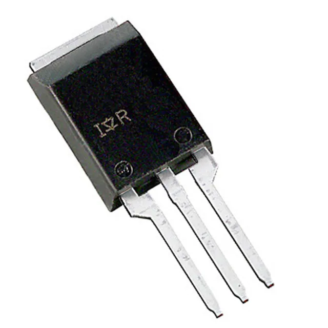
Same outline as TO-220
50% greater current in typ.
application conditions vs. TO-220
Fully Avalanche Rated
●
Purchase IRLBA1304/P for solder plated option.
l
l
l
l
D
VDSS = 40V
RDS(on) = 0.004Ω
G
ID = 185A
S
Description
The HEXFET® is the most popular power MOSFET in the world.
This particular HEXFET® is in the Super220TM and has the same outline and
pinout as the industry standard TO-220. It has increased current handling
capability over both the TO-220 and the much larger TO-247 package. This
makes it ideal to reduce component count in multiparalled TO-220 applications,
reduce system power dissipation, upgrade existing designs or have TO-247
performance in a TO-220 outline. This package has also been designed to meet
Super - 220
automotive qualification standard Q101.
Absolute Maximum Ratings
Parameter
ID @ TC = 25°C
ID @ TC = 100°C
IDM
PD @TC = 25°C
VGS
EAS
IAR
EAR
dv/dt
TJ
TSTG
Continuous Drain Current, VGS @ 10V
Continuous Drain Current, VGS @ 10V
Pulsed Drain Current
Power Dissipation
Linear Derating Factor
Gate-to-Source Voltage
Single Pulse Avalanche Energy
Avalanche Current
Repetitive Avalanche Energy
Peak Diode Recovery dv/dt
Operating Junction and
Storage Temperature Range
Soldering Temperature, for 10 seconds
Recommended clip force
Max.
Units
185, pkg limited to 95A*
130, pkg limited to 95A*
740
300
2.0
± 16
1160
100
30
5.0
-55 to + 175
A
W
W/°C
V
mJ
A
mJ
V/ns
°C
300 (1.6mm from case )
20
N
Thermal Resistance
Parameter
RθJC
RθCS
RθJA
Junction-to-Case
Case-to-Sink, Flat, Greased Surface
Junction-to-Ambient
Typ.
Max.
Units
–––
0.5
–––
0.5
–––
58
°C/W
* Current capability in normal application, see Fig.9.
www.irf.com
1
9/14/99
�IRLBA1304
Electrical Characteristics @ TJ = 25°C (unless otherwise specified)
∆V(BR)DSS/∆TJ
Parameter
Drain-to-Source Breakdown Voltage
Breakdown Voltage Temp. Coefficient
RDS(on)
Static Drain-to-Source On-Resistance
VGS(th)
gfs
Gate Threshold Voltage
Forward Transconductance
IDSS
Drain-to-Source Leakage Current
V(BR)DSS
Qg
Qgs
Qgd
td(on)
tr
td(off)
tf
Gate-to-Source Forward Leakage
Gate-to-Source Reverse Leakage
Total Gate Charge
Gate-to-Source Charge
Gate-to-Drain ("Miller") Charge
Turn-On Delay Time
Rise Time
Turn-Off Delay Time
Fall Time
LD
Internal Drain Inductance
LS
Internal Source Inductance
Ciss
Coss
Crss
Input Capacitance
Output Capacitance
Reverse Transfer Capacitance
IGSS
Min. Typ. Max. Units
Conditions
40
––– –––
V
VGS = 0V, ID = 250µA
––– 0.043 ––– V/°C Reference to 25°C, ID = 1mA
––– ––– 0.0040
VGS = 10V, ID = 110A
Ω
––– ––– 0.0065
VGS = 4.5V, ID = 93
1.0
––– –––
V
VDS = VGS, ID = 250µA
120 ––– –––
S
VDS = 25V, ID = 110A
––– ––– 25
VDS = 40V, VGS = 0V
µA
––– ––– 250
VDS = 32V, VGS = 0V, TJ = 150°C
––– ––– 100
VGS = 16V
nA
––– ––– -100
VGS = -16V
––– ––– 140
ID = 110A
––– ––– 39
nC
VDS = 32V
––– ––– 79
VGS = 4.5V, See Fig. 6 and 13
–––
21 –––
VDD = 20V
––– 350 –––
ID = 110A
–––
45 –––
RG = 0.9Ω
––– 103 –––
RD = 0.18Ω,See Fig. 10
Between lead,
–––
2.0 –––
nH
6mm (0.25in.)
G
from package
––– 5.0 –––
and center of die contact
––– 7660 –––
VGS = 0V
––– 2150 –––
pF
VDS = 25V
––– 460 –––
ƒ = 1.0MHz, See Fig. 5
D
S
Source-Drain Ratings and Characteristics
IS
ISM
VSD
trr
Qrr
ton
Parameter
Continuous Source Current
(Body Diode)
Pulsed Source Current
(Body Diode)
Diode Forward Voltage
Reverse Recovery Time
Reverse RecoveryCharge
Forward Turn-On Time
Notes:
Repetitive rating; pulse width limited by
max. junction temperature. ( See fig. 11 )
Starting TJ = 25°C, L = 230µH
Min. Typ. Max. Units
Conditions
D
MOSFET symbol
––– ––– 185*
showing the
A
G
integral reverse
––– ––– 740
S
p-n junction diode.
––– ––– 1.3
V
TJ = 25°C, IS = 110A, VGS = 0V
––– 100 150
ns
TJ = 25°C, IF = 110A
––– 250 380
nC
di/dt = 100A/µs
Intrinsic turn-on time is negligible (turn-on is dominated by LS+LD)
ISD ≤ 110A, di/dt ≤ 170A/µs, VDD ≤ V(BR)DSS,
TJ ≤ 175°C
Pulse width ≤ 300µs; duty cycle ≤ 2%.
RG = 25Ω, IAS = 100A. (See Figure 12)
2
www.irf.com
�IRLBA1304
1000
1000
VGS
15V
10V
5.0V
4.5V
3.5V
3.0V
2.7V
BOTTOM 2.5V
100
10
100
1
2.5V
0.1
0.1
20µs PULSE WIDTH
TJ = 25 °C
1
10
2.5V
100
2.5
R DS(on) , Drain-to-Source On Resistance
(Normalized)
TJ = 25 ° C
TJ = 175 ° C
100
10
1
V DS = 25V
20µs PULSE WIDTH
4.0
6.0
8.0
Fig 3. Typical Transfer Characteristics
www.irf.com
10
100
Fig 2. Typical Output Characteristics
1000
VGS , Gate-to-Source Voltage (V)
1
VDS , Drain-to-Source Voltage (V)
Fig 1. Typical Output Characteristics
0.1
2.0
20µs PULSE WIDTH
TJ = 175 °C
10
0.1
VDS , Drain-to-Source Voltage (V)
I D , Drain-to-Source Current (A)
VGS
15V
10V
5.0V
4.5V
3.5V
3.0V
2.7V
BOTTOM 2.5V
TOP
I D , Drain-to-Source Current (A)
I D , Drain-to-Source Current (A)
TOP
10.0
ID = 170A
2.0
1.5
1.0
0.5
0.0
-60 -40 -20
VGS = 10V
0
20 40 60 80 100 120 140 160 180
TJ , Junction Temperature ( °C)
Fig 4. Normalized On-Resistance
Vs. Temperature
3
�IRLBA1304
VGS = 0V,
f = 1MHz
Ciss = Cgs + Cgd , Cds SHORTED
Crss = Cgd
Coss = Cds + Cgd
C, Capacitance (pF)
10000
Ciss
8000
6000
4000
Coss
2000
15
VGS , Gate-to-Source Voltage (V)
12000
ID = 110A
VDS = 32V
VDS = 20V
VDS = 8V
12
9
6
3
Crss
0
1
10
FOR TEST CIRCUIT
SEE FIGURE 13
0
100
0
VDS , Drain-to-Source Voltage (V)
40
80
120
160
200
Q G , Total Gate Charge (nC)
Fig 6. Typical Gate Charge Vs.
Gate-to-Source Voltage
Fig 5. Typical Capacitance Vs.
Drain-to-Source Voltage
1000
10000
I D , Drain Current (A)
ISD , Reverse Drain Current (A)
OPERATION IN THIS AREA LIMITED
BY RDS(on)
TJ = 175 ° C
1000
100
V GS = 0 V
0.6
0.8
1.0
1.2
1.4
1.6
VSD ,Source-to-Drain Voltage (V)
Fig 7. Typical Source-Drain Diode
Forward Voltage
4
100us
100
TJ = 25 ° C
10
0.4
10us
1.8
1ms
TC = 25 ° C
TJ = 175 ° C
Single Pulse
10
1
10ms
10
100
VDS , Drain-to-Source Voltage (V)
Fig 8. Maximum Safe Operating Area
www.irf.com
�IRLBA1304
200
RD
VDS
LIMITED BY PACKAGE
VGS
I D , Drain Current (A)
160
D.U.T.
RG
+
-VDD
120
4.5V
Pulse Width ≤ 1 µs
Duty Factor ≤ 0.1 %
80
Fig 10a. Switching Time Test Circuit
40
VDS
90%
0
25
50
75
100
125
150
175
TC , Case Temperature ( ° C)
10%
VGS
Fig 9. Maximum Drain Current Vs.
Case Temperature
td(on)
tr
t d(off)
tf
Fig 10b. Switching Time Waveforms
Thermal Response (Z thJC )
1
D = 0.50
0.1
0.20
0.10
0.05
0.02
0.01
0.01
P DM
SINGLE PULSE
(THERMAL RESPONSE)
t1
t2
Notes:
1. Duty factor D = t 1 / t 2
2. Peak T J = P DM x Z thJC + TC
0.001
0.00001
0.0001
0.001
0.01
0.1
1
t1 , Rectangular Pulse Duration (sec)
Fig 11. Maximum Effective Transient Thermal Impedance, Junction-to-Case
www.irf.com
5
�IRLBA1304
1 5V
L
VDS
D .U .T
RG
IA S
20V
ID
41A
71A
BOTTOM 100A
TOP
2500
2000
D R IV E R
1500
+
V
- DD
A
1000
0 .0 1 Ω
tp
EAS , Single Pulse Avalanche Energy (mJ)
3000
Fig 12a. Unclamped Inductive Test Circuit
500
0
25
50
75
100
125
150
175
Starting TJ , Junction Temperature ( °C)
V (B R )D SS
tp
Fig 12c. Maximum Avalanche Energy
Vs. Drain Current
IAS
Current Regulator
Same Type as D.U.T.
Fig 12b. Unclamped Inductive Waveforms
50KΩ
QG
12V
.2µF
.3µF
4.5 V
QGS
+
V
- DS
VGS
VG
3mA
Charge
Fig 13a. Basic Gate Charge Waveform
6
D.U.T.
QGD
IG
ID
Current Sampling Resistors
Fig 13b. Gate Charge Test Circuit
www.irf.com
�IRLBA1304
Peak Diode Recovery dv/dt Test Circuit
+
D.U.T
Circuit Layout Considerations
• Low Stray Inductance
• Ground Plane
• Low Leakage Inductance
Current Transformer
+
-
-
+
•
•
•
•
RG
dv/dt controlled by RG
Driver same type as D.U.T.
ISD controlled by Duty Factor "D"
D.U.T. - Device Under Test
Driver Gate Drive
P.W.
D=
Period
+
-
VDD
P.W.
Period
VGS=10V
*
D.U.T. ISD Waveform
Reverse
Recovery
Current
Body Diode Forward
Current
di/dt
D.U.T. VDS Waveform
Diode Recovery
dv/dt
Re-Applied
Voltage
Body Diode
VDD
Forward Drop
Inductor Curent
Ripple ≤ 5%
ISD
* VGS = 5V for Logic Level Devices
Fig 14. For N-Channel HEXFETS
www.irf.com
7
�IRLBA1304
Super-220 Package Outline
WORLD HEADQUARTERS: 233 Kansas St., El Segundo, California 90245, Tel: (310) 322 3331
IR GREAT BRITAIN: Hurst Green, Oxted, Surrey RH8 9BB, UK Tel: ++ 44 1883 732020
IR CANADA: 15 Lincoln Court, Brampton, Ontario L6T3Z2, Tel: (905) 453 2200
IR GERMANY: Saalburgstrasse 157, 61350 Bad Homburg Tel: ++ 49 6172 96590
IR ITALY: Via Liguria 49, 10071 Borgaro, Torino Tel: ++ 39 11 451 0111
IR FAR EAST: K&H Bldg., 2F, 30-4 Nishi-Ikebukuro 3-Chome, Toshima-Ku, Tokyo Japan 171 Tel: 81 3 3983 0086
IR SOUTHEAST ASIA: 1 Kim Seng Promenade, Great World City West Tower, 13-11, Singapore 237994 Tel: ++ 65 838 4630
IR TAIWAN:16 Fl. Suite D. 207, Sec. 2, Tun Haw South Road, Taipei, 10673, Taiwan Tel: 886-2-2377-9936
http://www.irf.com/
Data and specifications subject to change without notice. 9/99
8
www.irf.com
�