PD - 97146A
IRLR8726PbF
IRLU8726PbF
HEXFET® Power MOSFET
Applications
l High Frequency Synchronous Buck
VDSS
RDS(on) max
Qg (typ.)
Converters for Computer Processor Power
30V 5.8m @VGS = 10V 15nC
l High Frequency Isolated DC-DC
Converters with Synchronous Rectification
D
D
for Telecom and Industrial Use
:
Benefits
l Very Low RDS(on) at 4.5V VGS
l Ultra-Low Gate Impedance
l Fully Characterized Avalanche Voltage
and Current
l Lead-Free
l RoHS compliant
G
D
S
G
D-Pak
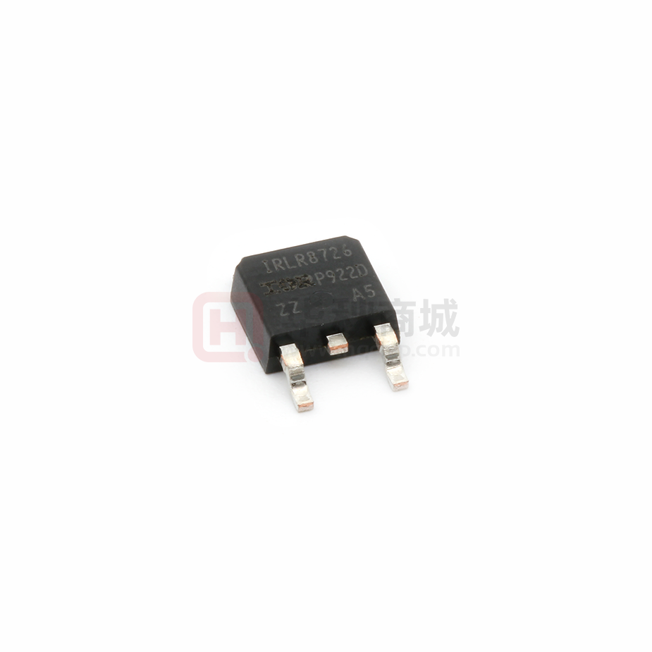
IRLR8726PbF
D
S
I-Pak
IRLU8726PbF
G
D
S
Gate
Drain
Source
Absolute Maximum Ratings
Max.
Units
Drain-to-Source Voltage
Gate-to-Source Voltage
Continuous Drain Current, VGS @ 10V
Parameter
30
± 20
86
V
61
A
IDM
Continuous Drain Current, VGS @ 10V
Pulsed Drain Current
VDS
VGS
ID @ TC = 25°C
ID @ TC = 100°C
c
PD @TC = 25°C
Maximum Power Dissipation
PD @TC = 100°C
Maximum Power Dissipation
TJ
Linear Derating Factor
Operating Junction and
TSTG
Storage Temperature Range
f
f
340
h
h
W
75
38
W/°C
°C
0.5
-55 to + 175
Soldering Temperature, for 10 seconds
300 (1.6mm from case)
Thermal Resistance
Parameter
h
RθJC
Junction-to-Case
RθJA
Junction-to-Ambient (PCB Mount)
RθJA
Junction-to-Ambient
h
gh�
Typ.
Max.
–––
2.0
–––
50
–––
110
Units
°C/W
Notes through are on page 11
ORDERING INFORMATION:
See detailed ordering and shipping information on the last page of this data sheet.
www.irf.com
1
11/23/09
�IRLR/U8726PbF
Static @ TJ = 25°C (unless otherwise specified)
Parameter
Min. Typ. Max. Units
BVDSS
Drain-to-Source Breakdown Voltage
∆ΒVDSS/∆TJ
Breakdown Voltage Temp. Coefficient
RDS(on)
Static Drain-to-Source On-Resistance
30
V
–––
–––
20
–––
–––
4.0
5.8
mV/°C Reference to 25°C, ID = 1mA
mΩ VGS = 10V, ID = 25A
–––
5.8
8.0
VGS = 4.5V, ID = 20A
Gate Threshold Voltage
1.35
1.80
2.35
V
∆VGS(th)/∆TJ
Gate Threshold Voltage Coefficient
–––
-8.6
–––
mV/°C
IDSS
Drain-to-Source Leakage Current
–––
–––
1.0
µA
–––
–––
150
Gate-to-Source Forward Leakage
–––
–––
100
Gate-to-Source Reverse Leakage
–––
–––
-100
gfs
Forward Transconductance
73
–––
–––
Qg
Total Gate Charge
–––
15
23
VGS = 0V, ID = 250µA
e
e
VGS(th)
IGSS
Conditions
–––
VDS = VGS, ID = 50µA
VDS = 24V, VGS = 0V
VDS = 24V, VGS = 0V, TJ = 125°C
nA
VGS = 20V
VGS = -20V
S
VDS = 15V, ID = 20A
VDS = 15V
Qgs1
Pre-Vth Gate-to-Source Charge
–––
3.7
–––
Qgs2
Post-Vth Gate-to-Source Charge
–––
1.9
–––
Qgd
Gate-to-Drain Charge
–––
5.7
–––
ID = 20A
Qgodr
Gate Charge Overdrive
–––
3.7
–––
See Fig. 15
Qsw
Switch Charge (Qgs2 + Qgd)
–––
7.6
–––
Qoss
Output Charge
–––
10
–––
nC
RG
Gate Resistance
–––
2.0
3.5
Ω
td(on)
Turn-On Delay Time
–––
12
–––
VDD = 15V, VGS = 4.5V
tr
Rise Time
–––
49
–––
td(off)
Turn-Off Delay Time
–––
15
–––
ID = 20A
RG = 1.8Ω
tf
Fall Time
–––
16
–––
See Fig. 13
Ciss
Input Capacitance
–––
2150
–––
VGS = 0V
Coss
Output Capacitance
–––
480
–––
Crss
Reverse Transfer Capacitance
–––
205
–––
nC
ns
pF
VGS = 4.5V
VDS = 15V, VGS = 0V
e
VDS = 15V
ƒ = 1.0MHz
Avalanche Characteristics
EAS
Parameter
Single Pulse Avalanche Energy
IAR
Avalanche Current
�c
d
Typ.
Max.
Units
–––
120
mJ
–––
20
A
Diode Characteristics
Parameter
Min. Typ. Max. Units
f
Conditions
IS
Continuous Source Current
–––
–––
86
ISM
(Body Diode)
Pulsed Source Current
–––
–––
340
VSD
(Body Diode)
Diode Forward Voltage
–––
–––
1.0
V
p-n junction diode.
TJ = 25°C, IS = 20A, VGS = 0V
trr
Reverse Recovery Time
–––
24
36
ns
TJ = 25°C, IF = 20A, VDD = 15V
Qrr
Reverse Recovery Charge
–––
52
78
nC
di/dt = 300A/µs
2
�c
MOSFET symbol
A
showing the
integral reverse
e
e
www.irf.com
�IRLR/U8726PbF
1000
1000
100
BOTTOM
TOP
ID, Drain-to-Source Current (A)
ID, Drain-to-Source Current (A)
TOP
VGS
10V
5.0V
4.5V
3.5V
3.3V
3.0V
2.7V
2.5V
10
1
≤ 60µs PULSE WIDTH
Tj = 25°C
100
BOTTOM
10
2.5V
≤ 60µs PULSE WIDTH
Tj = 175°C
2.5V
0.1
1
0.1
1
10
100
0.1
VDS, Drain-to-Source Voltage (V)
1
10
100
VDS, Drain-to-Source Voltage (V)
Fig 1. Typical Output Characteristics
Fig 2. Typical Output Characteristics
2.0
RDS(on) , Drain-to-Source On Resistance
(Normalized)
1000
ID, Drain-to-Source Current (A)
VGS
10V
5.0V
4.5V
3.5V
3.3V
3.0V
2.7V
2.5V
100
10
TJ = 175°C
TJ = 25°C
1
VDS = 15V
≤ 60µs PULSE WIDTH
0.1
0.0
2.0
4.0
6.0
VGS, Gate-to-Source Voltage (V)
Fig 3. Typical Transfer Characteristics
www.irf.com
8.0
ID = 25A
VGS = 10V
1.5
1.0
0.5
-60 -40 -20
0
20 40 60 80 100 120 140 160 180
TJ , Junction Temperature (°C)
Fig 4. Normalized On-Resistance
vs. Temperature
3
�IRLR/U8726PbF
12
VGS = 0V,
f = 1 MHZ
Ciss = Cgs + Cgd, Cds SHORTED
Crss = Cgd
VGS, Gate-to-Source Voltage (V)
C, Capacitance (pF)
10000
Coss = Cds + Cgd
Ciss
1000
Coss
Crss
ID= 20A
VDS= 24V
VDS= 15V
10
8
6
4
2
0
100
1
10
0
100
4
Fig 6. Typical Gate Charge vs.
Gate-to-Source Voltage
Fig 5. Typical Capacitance vs.
Drain-to-Source Voltage
10000
ID, Drain-to-Source Current (A)
ISD , Reverse Drain Current (A)
1000
TJ = 175°C
100
10
12 16 20 24 28 32 36 40
QG Total Gate Charge (nC)
VDS , Drain-to-Source Voltage (V)
TJ = 25°C
1
OPERATION IN THIS AREA
LIMITED BY R DS(on)
1000
100µsec
100
1msec
10msec
10
1
VGS = 0V
TC= 25°C
TJ = 175°C
Single Pulse
0.1
0.1
0.2
0.4
0.6
0.8
1.0
1.2
1.4
1.6
1.8
VSD , Source-to-Drain Voltage (V)
Fig 7. Typical Source-Drain Diode
Forward Voltage
4
8
2.0
0.1
1
10
100
VDS, Drain-toSource Voltage (V)
Fig 8. Maximum Safe Operating Area
www.irf.com
�IRLR/U8726PbF
100
2.5
VGS(th) Gate threshold Voltage (V)
LIMITED BY PACKAGE
ID , Drain Current (A)
80
60
40
20
0
25
50
75
100
125
150
ID = 500µA
ID = 50µA
ID = 25µA
2.0
1.5
1.0
0.5
175
-75 -50 -25
TC , Case Temperature (°C)
0
25
50
75
100 125 150 175
TJ , Temperature ( °C )
Fig 9. Maximum Drain Current vs.
Case Temperature
Fig 10. Threshold Voltage vs. Temperature
Thermal Response ( ZthJC )
10
1
D = 0.50
0.20
0.10
0.05
0.02
0.1
τJ
0.01
R1
R1
τJ
τ1
R2
R2
R4
R4
τC
τ1
τ2
τ2
Ci= τi/Ri
Ci i/Ri
0.01
R3
R3
SINGLE PULSE
( THERMAL RESPONSE )
τ3
τ3
τ4
τ4
τ
Ri (°C/W) τι (sec)
0.014297 0.000003
0.373312 0.00009
1.010326 0.000973
0.602065 0.007272
Notes:
1. Duty Factor D = t1/t2
2. Peak Tj = P dm x Zthjc + Tc
0.001
1E-006
1E-005
0.0001
0.001
0.01
0.1
t1 , Rectangular Pulse Duration (sec)
Fig 11. Maximum Effective Transient Thermal Impedance, Junction-to-Case
www.irf.com
5
�EAS, Single Pulse Avalanche Energy (mJ)
IRLR/U8726PbF
500
I D
5.6A
8.2A
BOTTOM 20A
TOP
400
300
200
100
0
25
50
75
100
125
150
175
Starting TJ , Junction Temperature (°C)
Fig 12a. Maximum Avalanche Energy
Vs. Drain Current
V(BR)DSS
15V
D.U.T
RG
20V
VGS
DRIVER
L
VDS
tp
+
V
- DD
IAS
tp
A
0.01Ω
I AS
Fig 12b. Unclamped Inductive Test Circuit
V DS
VGS
RG
RD
VDS
90%
D.U.T.
+
-VDD
V GS
Pulse Width ≤ 1 µs
Duty Factor ≤ 0.1 %
Fig 13a. Switching Time Test Circuit
6
Fig 12c. Unclamped Inductive Waveforms
10%
VGS
td(on)
tr
t d(off)
tf
Fig 13b. Switching Time Waveforms
www.irf.com
�IRLR/U8726PbF
Driver Gate Drive
D.U.T
P.W.
+
+
-
-
*
RG
•
•
•
•
***
D.U.T. ISD Waveform
Reverse
Recovery
Current
+
dv/dt controlled by RG
Driver same type as D.U.T.
I SD controlled by Duty Factor "D"
D.U.T. - Device Under Test
V DD
**
P.W.
Period
VGS=10V
Circuit Layout Considerations
• Low Stray Inductance
• Ground Plane
• Low Leakage Inductance
Current Transformer
D=
Period
+
Body Diode Forward
Current
di/dt
D.U.T. VDS Waveform
Diode Recovery
dv/dt
Re-Applied
Voltage
-
Body Diode
VDD
Forward Drop
Inductor Curent
ISD
Ripple ≤ 5%
* Use P-Channel Driver for P-Channel Measurements
** Reverse Polarity for P-Channel
*** VGS = 5V for Logic Level Devices
Fig 14. Diode Reverse Recovery Test Circuit for HEXFET® Power MOSFETs
Id
Vds
Vgs
L
DUT
0
20K
1K
VCC
Vgs(th)
S
Qgodr
Fig 15. Gate Charge Test Circuit
www.irf.com
Qgd
Qgs2 Qgs1
Fig 16. Gate Charge Waveform
7
�IRLR/U8726PbF
D-Pak (TO-252AA) Package Outline
Dimensions are shown in millimeters (inches)
D-Pak (TO-252AA) Part Marking Information
(;$03/(�
7+,6�,6�$1�,5)5���
3$57�180%(5
:,7+�$66(0%/<
,17(51$7,21$/
/27�&2'(�����
,5)5���
���$
��
��
5(&7,),(5
$66(0%/('�21�::���������
/2*2
,1�7+(�$66(0%/