IRPS5401 PMIC Datasheet
IRPS5401 PMIC
Flexible Power Management Unit
Features
Full power system including 5 integrated outputs
4A, 4A, 2A and 2A Switching Regulators
500mA Source/Sink Linear regulator
Single rail operation 5.5V to 12V
Output Range from 0.25V to 5.1V for outputs A-D and 0.5V to 3.6V for LDO
Allows combining outputs and/or the use of an external IR MOSFET™ Power Stage to increase output
current to as high as 50A
Emulated current mode control without external compensation
Differential voltage sensing on Switcher A for higher accuracy
I2C / PMBus with integrated level shifter
Advanced Sequencing control
Extensive PMBus command set of 74 commands
Integrated current sensing and full telemetry including voltage, current, temperature and faults
Rated for -40°C to +125°C TJ operation
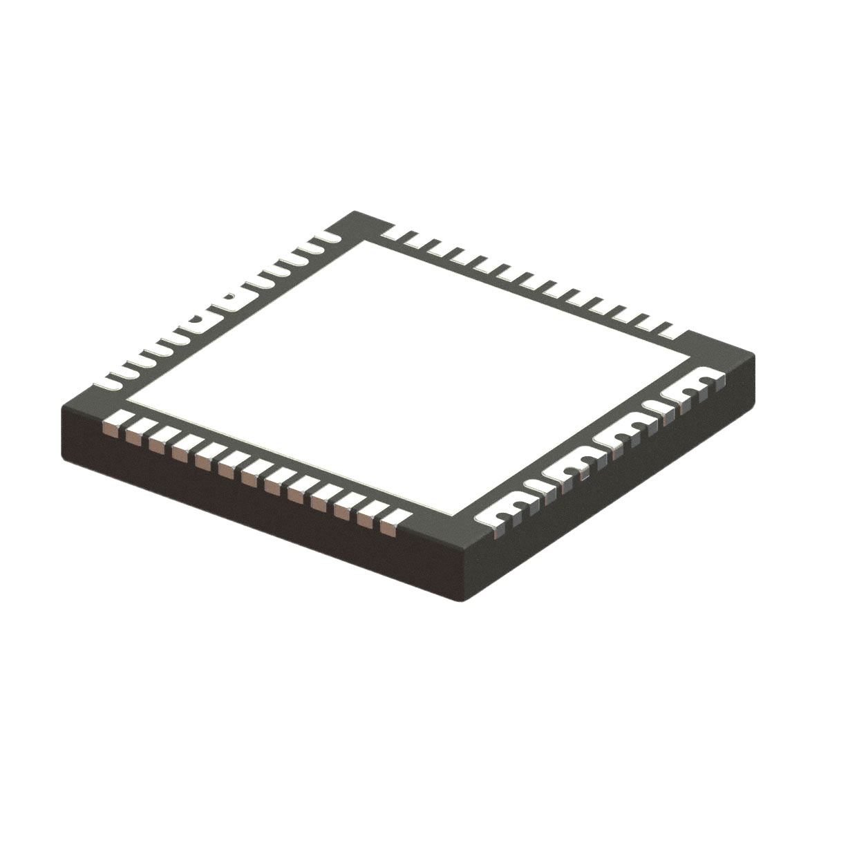
Pb-Free, RoHS6, 7x7mm, 56-pin, 0.4mm pitch QFN
Potential applications
High density ASIC, FPGA & CPU multi-rail systems
Embedded Computing systems
Communications and Storage systems
Description
The IRPS5401 is a complete power management unit delivering up to 5 output voltages to processors, FPGA’s
and other multi-rail power systems. Four high efficiency configurable switching regulators and a Source/Sink
Linear regulator provide the typical rails required such as core voltage, memory voltage and I/O voltages.
Integrated, accurate current, voltage and temperature sensing allows telemetry and fault reporting through the
I2C/PMBus.
The IRPS5401 switching regulators utilize fixed frequency emulated current mode control, and thus no external
compensation is required.
The IRPS5401 is highly flexible. Switchers A and B deliver 2A each. Switchers C and D, deliver 4A each and can
also be combined to deliver 8A. Further, Switcher A can be configured to use an external IR MOSFET™ Power
Stage to deliver up to 50A or more.
Datasheet
www.infineon.com
Please read the Important Notice and Warnings at the end of this document
page 1 of 64
V 2.6
2021-01-11
�IRPS5401 PMIC
Flexible Power Management Unit
Table of contents
Table of contents
Features ........................................................................................................................................ 1
Potential applications ..................................................................................................................... 1
Description .................................................................................................................................... 1
Table of contents ............................................................................................................................ 2
1
Ordering Information ............................................................................................................. 4
2
Application Circuit.................................................................................................................. 6
3
Pinout Diagram ...................................................................................................................... 7
4
Pin Function .......................................................................................................................... 8
5
Block Diagram ...................................................................................................................... 11
6
Absolute Maximum Ratings .................................................................................................... 12
7
Electrical Specifications ......................................................................................................... 13
8
Typical Application Diagrams ................................................................................................. 20
9
Description ........................................................................................................................... 24
9.1
One-time Programmable (OTP) Memory ............................................................................................. 24
9.2
MTP pin (pin 54) ..................................................................................................................................... 24
9.3
Device Power-up and Initialization....................................................................................................... 25
9.4
Addressing the IRPS5401 ...................................................................................................................... 26
9.5
Switching Frequency ............................................................................................................................. 27
9.6
Synchronizing to an External Clock ...................................................................................................... 28
9.7
Switcher A in External Powerstage Mode ............................................................................................. 28
9.8
Digital Controller & PWM ....................................................................................................................... 29
9.9
Diode Emulation / Discontinuous Mode Operation/AOT ..................................................................... 30
9.10
Output Voltage Sensing, Telemetry and Faults ................................................................................... 30
9.11
Output Over Voltage Protection (OVP) ................................................................................................. 31
9.12
Output Under Voltage Protection (UVP) ............................................................................................... 32
9.13
Current Sensing, Telemetry and Faults ................................................................................................ 33
9.14
Over-current Protection (OCP) ............................................................................................................. 34
9.15
Input Voltage Sensing, Telemetry and Faults ...................................................................................... 35
9.16
Die Temperature Sensing, Telemetry and Faults ................................................................................. 36
9.17
Power Sequencing and Global Faults ................................................................................................... 36
9.18
Sleep ...................................................................................................................................................... 38
9.19
Combined Switcher C and D Operation................................................................................................ 38
9.20
Linear Regulator .................................................................................................................................... 38
9.21
LDO Monitoring and Faults ................................................................................................................... 39
9.22
Output Voltage Reporting, Output Overvoltage Protection and Undervoltage Protection ............... 39
9.23
Input Voltage Reporting, Input UVLO and Input Overvoltage Protection ........................................... 39
9.24
Over Current Protection ........................................................................................................................ 39
9.25
I2C Security ............................................................................................................................................ 40
9.26
Password Protection ............................................................................................................................. 41
9.27
Pin Protection ........................................................................................................................................ 41
10
Layout Guidelines ................................................................................................................. 43
10.1
Sample layout........................................................................................................................................ 44
11
Typical Performance ............................................................................................................. 47
11.1
Typical thermal performance at max output power............................................................................ 48
12
PMBUS Commands ................................................................................................................ 49
Datasheet
2 of 64
V 2.6
2021-01-11
�IRPS5401 PMIC
Flexible Power Management Unit
Table of contents
13
Marking Information ............................................................................................................. 55
14
Package Information ............................................................................................................. 56
14.1
PCB Pad Size .......................................................................................................................................... 57
14.2
PCB Pad Spacing ................................................................................................................................... 58
14.3
Solder Paste Stencil Pad Size................................................................................................................ 59
14.4
Solder Paste Stencil Pad Spacing ......................................................................................................... 60
15
Environmental Qualifications ................................................................................................. 61
Revision History ............................................................................................................................ 62
Datasheet
3 of 64
V 2.6
2021-01-11
�IRPS5401 PMIC
Flexible Power Management Unit
Ordering Information
1
Ordering Information
Table 1
Ordering Information
Base part
number
Package type
Standard pack Orderable part number
Description
IRPS5401M
QFN 7 mm x 7 mm
Tape and Reel
IRPS5401MTRPBF
Unprogrammed
IRPS5401M
QFN 7 mm x 7 mm
Tape and Reel
IRPS5401MXI03TRP
Pre-programmed per
Table 2
IRPS5401M
QFN 7 mm x 7 mm
Tape and Reel
IRPS5401MXI04TRPAUMA1
Pre-programmed per
Table 3
Table 2
IRPS5401MXI03TRP Loop Configurations
Config
R_MTP
R_ADDR
A (bold =
external PS)
B
C
D
LDO
(supplied from)
1
8.87kΩ
1.8V/0.5A
1.8V/1.4A
0.85V/0.6A
0.85V/3.7A
1.2V (B)
2
10kΩ
1.2V/1.2A
0.85V/0.6A
3.3V/1.5A
0.85V/4A
1.8V (C)
3
11kΩ
1.8V/0.5A
5V/1.5A
3.3V/3.3A
0.85V/2A
1.8V (C)
4
2.32kΩ
0.85V/16A
1.2V/1.5A
1.8V/1A
1.8V/4A
1.2V (D or external)
5
2.87kΩ
0.85V/25A
1.2V/1.5A
1.8V/1A
1.8V/4A
1.2V (D or external)
6
3.48kΩ
3.3V/1.4A
1.8V/1A
0.9V/3A
1.2V/3A
0.85V (A)
7
4.12kΩ
0.72V/9A
3.3V/2A
0.85V/7A
1.2V (B)
8
4.75kΩ
0.72V/15A
3.3V/2A
0.85V/7A
1.2V (B)
9
5.49kΩ
1.8V/1A
1.2V/1.5A
1.8V/4A
2.5V/1.5A
1.8V (D)
10
6.19kΩ
0.9V/2A
1.2V/1.5A
1.8V/2.5A
1.2V/2A
0.85V (C)
11
6.98kΩ
0.72V/9A
1.2V/1.5A
0.85V/4A
1.8V/2A
1.2V (D or external)
12
7.87kΩ
0.72V/20A
1.2V/1.2A
0.85V/4A
1.8V/2A
1.2V (D or external)
Datasheet
4 of 64
V 2.6
2021-01-11
�IRPS5401 PMIC
Flexible Power Management Unit
Ordering Information
Table 3
IRPS5401MXI04TRPAUMA1 Loop Configurations
Config
R_MTP
R_ADDR
A (bold =
external PS)
B
C
1
Not
used
2
Not
used
3
Not
used
4
2.32kΩ
0.85V/ 15A
1.8V/2A
1.2V/5A
5
2.87kΩ
3.3V/10A
1.13V/1A
5V/2.1A
6
3.48kΩ
0.85V/15A
1.8V/2A
0.85V/7A
3.3V/0.5A (optional)
7
4.12kΩ
3.3V/10A
2.5V/2A
1.2V/6A
0.85V/0.5A
(external 2.5V)
8
4.75kΩ
1.2V/6A
2.5V/0.5A
1.8V/5A
1.8V/0.5A
(external 2.5V)
Datasheet
5 of 64
D
LDO
(supplied from)
0.9V/0.5A
(external 2.5V)
1.8V/3A
0.85V/0.5A (external
2.5V)
V 2.6
2021-01-11
�IRPS5401 PMIC
Flexible Power Management Unit
Application Circuit
2
Application Circuit
6-12V
BOOT_C
BOOT_A
PHASE_C
PHASE_A
VOUT_C
VOUT_A
2A
4A
BOOT_B
BOOT_D
VOUT_B
VOUT_D
PHASE_B
PHASE_D
4A
1.2V to 5.5V
2A
1.8V
VIN_LDO
5V
500mA
VO_LDO
V
V
V
ADDR_PROT
GND
5
5
SYNC_IN
MTP
Figure 1
IRPS5401 Basic application circuit
Figure 2
System efficiency with VO= 2.5V, FSW=800kHz, Tj=45°C
Datasheet
6 of 64
V
EN
V
PG
ALERT#
CLK
DATA
V
I2C /
PMBus
VDDIO
V
SLEEP#
1.8V – 5V
V 2.6
2021-01-11
�IRPS5401 PMIC
Flexible Power Management Unit
Pinout Diagram
VIN_D
BOOT_D
PHASE_D
ADDR_PROT
MTP
EN_D
SYNC_CLK
EN_C
AGND
VSUPPLY
VCC
VDRV
ISEN_A+
ISEN_A-
EN_B
PWM_A
Pinout Diagram
FB_D
3
56
55
54
53
52
51
50
49
48
47
46
45
44
43
1
42
EN_A
2
41
FB _A
3
40
RTN_A
4
39
VIN_A
5
38
BOOT_A
6
37
8
PHASE_C
BOOT_C
VIN_C
PHASE_A
IRPS5401
56 Pin 7x 7 Pin QFN
0.4 mm Pitch
7
36
35
PHASE_B
9
34
10
33
BOOT_B
11
32
VIN_B
12
31
FB_B
13
30
PG_B
29
SLEEP#
57 GND
14
25
26
27
28
EN_L
VDDIO
24
PG_C
DATA
23
PG_A
CLK
22
PG_L
ALERT#
21
FB _L
20
VO_LDO
19
VIN_LDO
18
1V8
17
PG_D
Datasheet
16
FB_C
Figure 3
15
Pinout diagram 7mm x 7mm QFN (Top View)
7 of 64
V 2.6
2021-01-11
�IRPS5401 PMIC
Flexible Power Management Unit
Pin Function
4
Pin Function
Table 4
PIN Function
PIN
#
Name
Description
If not used
TYP
1,2,3
VIN_D
P [I]
Input supply voltage pins for Switcher D. Decouple locally by
connecting a ceramic capacitor from this pin to GND.
Short To
GND
4
BOOT_D
A [B]
Supply input for Switcher D high side FET gate drive. Connect
a 0.1uF MLCC between this pin and PHASE_ D pins. An
internal diode is connected between VDRV and this pin
Open
5,6,7
PHASE_D
P [O]
Switch node of Switcher D. Connect directly to the output
inductor.
Open
8,9,
10
PHASE_C
P [O]
Switch node of Switcher C. Connect directly to the output
inductor.
Open
11
BOOT_C
A [B]
Supply input for Switcher C high side FET gate drive. Connect
a 0.1uF MLCC between this pin and PHASE_C pins. An internal
diode is connected between VDRV and this pin
Open
12,
13,14
VIN_C
P [I]
Input supply voltage pins for Switcher C. Decouple locally by
connecting a ceramic capacitor from this pin to GND.
Short To
GND
15
FB_C
A [I]
Switcher C feedback input. Connect directly to VOUT_C for
output voltages less than 2.55V. Connect to VOUT_C with a
2:1 resistor divider for output voltages greater than 2.55V.
Open
16
PG_D
D [O]
Open drain power good output indicating Switcher D is
powered up
Open
17
ALERT#
D [O]
I2C/PMBus Alert line. This alert signal can indicate one or
more faults, allowing the system bus manager to poll the
device and identify the root cause. All faults or customer
selected faults such as overcurrent or over-temperature may
be specifically masked to this pin.
Open
18
CLK
D [B]
I2C/PMBus Clock Line. Pull up to VDDIO with 10K
n/a
19
DATA
D [B]
I2C/PMBus Data Line. Pull up to VDDIO with 10K
n/a
20
VDDIO
P [I]
Pull-up signal voltage for I2C communications. Connect to the
same I/O rail used by the I2C master.
n/a
21
1V8
A [O]
1.8V reference used by the device for internal analog and
digital control. Decouple using a 1.0uF X7R type ceramic
capacitor
n/a
22
VIN_LDO
P [I]
Input to the linear regulator. See linear regulator section for
specific requirements. This voltage can range from 1.2V to
5.5V, with restrictions on overall power dissipation
Short To
GND
23
VO_LDO
A[O]
LDO output
Open
24
FB_L
A [I]
LDO feedback input
Open
25
PG_L
D[I]
Open drain power good output indicating LDO is powered up.
Pull up to 5V with 10K
Open
26
PG_A
D[I]
Open drain power good output indicating switcher A is
powered up. Pull up to 5V with 10K
Open
Datasheet
8 of 64
V 2.6
2021-01-11
�IRPS5401 PMIC
Flexible Power Management Unit
Pin Function
PIN
#
Name
Description
If not used
TYP
27
PG_C
D[I]
Open drain power good output indicating switcher C is
powered up. Pull up to 5V with 10K
Open
28
EN_L
D[I]
LDO enable input control. Active High, external termination
required, do not leave floating. LVTTL threshold levels. ‘ON’
threshold is 2.1V minimum
Short To
GND
29
SLEEP#
D[I]
Active low signal to place the device in a low power mode
LVTTL threshold levels. ‘SLEEP ENABLED’ threshold is 0.8V
maximum
Short to
VCC
30
PG_B
D[I]
Open drain power good output indicating switcher B is
powered up. Pull up to 5V with 10K
Open
31
FB_B
A [I]
Switcher B feedback input. Connect directly to VOUT_B for
output voltages less than 2.55V. Connect to VOUT_B with a
2:1 resistor divider for output voltages greater than 2.55V.
Open
32
VIN_B
P [I]
Input supply voltage pin for Switcher B. Decouple locally by
connecting a ceramic capacitor from this pin to GND.
Short To
GND
33
BOOT_B
A [B]
Supply input for Switcher B high side FET gate drive. Connect
a 0.1uF MLCC between this pin and PHASE_ B pins. An
internal diode is connected between VDRV and this pin
Open
34,35
PHASE_B
P [O]
Switch node of Switcher B. Connect directly to the output
inductor.
Open
36,37
PHASE_A
P [O]
Switch node of Switcher A. Connect directly to the output
inductor.
Open
38
BOOT_A
A [B]
Supply input for Switcher A high side FET gate drive. Connect
a 0.1uF MLCC between this pin and PHASE_A pins. An internal
diode is connected between VDRV and this pin
Open
39
VIN_A
P [I]
Input supply voltage pin for Switcher A. Decouple locally by
connecting a ceramic capacitor from this pin to GND.
Short To
GND
40
RTN_A
A [I]
Differential feedback return signal for Switcher A. This can be
connected remotely to the return location of VOUT_A.
Short
together
41
FB_A
A [I]
Differential feedback positive signal for Switcher A. Connect
directly to VOUT_A for output voltages less than 2.55V.
Connect to VOUT_A with a 2:1 resistor divider for output
voltages greater than 2.55V.
Short
together
42
EN_A
D [I]
Switcher A enable input control; external termination
required, do not leave floating. LVTTL threshold levels. ‘ON’
threshold is 2.1V minimum
Short To
GND
43
PWM_A
A [O]
PWM signal for Switcher A to be used when Switcher A is
configured for use with an external IR MOSFET™ Power
Stage. This PWM pin is a 5V PWM. This pin is used to drive a
5V capable external power stage such as an IR355x power
stage and is a tri-state or tri-level signal. A resistor and zener
clamp must be used when paired with a 3.3V only power stage
(see figure 11). Leave floating if this pin is not used
Open
Switcher B enable input control; external termination
required, do not leave floating. LVTTL threshold levels. ‘ON’
Short To
GND
44
Datasheet
EN_B
D [I]
9 of 64
V 2.6
2021-01-11
�IRPS5401 PMIC
Flexible Power Management Unit
Pin Function
PIN
#
Name
Description
If not used
TYP
threshold is 2.1V minimum
45
ISEN_A-
A[I]
Negative (return) sense point for Switcher A external IOUT
sense.
Short
together
46
ISEN_A+
A[I]
Positive sense point for Switcher A external IOUT sense.
Short
together
47
VDRV
A [O]
5V drive voltage used to power the internal MOSFET drivers.
Use a 2.2Ω, 2.2uF filter from VCC to insure noise from this
switching node is not injected into the VCC pin. See the
application section. Terminate decoupling cap to GND (pin 57)
n/a
5V source used by the device to power internal analog and
digital control. When VCC is self-generated by the device (from
VSUPPLY), do not load this pin with any load other than VDRV.
Decouple using a 2.2uF X7R type ceramic capacitor.
Terminate decoupling cap to AGND (pin 50)
n/a
48
VCC
A [O]
Input voltage for internal LDO for internally generated VCC
Short to
VCC
Ground reference for the analog and digital control.
n/a
D[I]
Switcher C enable input control; external termination
required, do not leave floating. LVTTL threshold levels. ‘ON’
threshold is 2.1V minimum
Short To
GND
SYNC_CLK
D[I]
External Synchronization pin. LVTTL threshold levels. ‘HIGH’
threshold is 2.1V minimum, ‘LOW’ is 0.8V maximum
Short to
GND
53
EN_D
D [I]
Switcher D enable input control; external termination
required, do not leave floating. LVTTL threshold levels. ‘ON’
threshold is 2.1V minimum
Short to
GND
54
MTP
A [I]
A resistor placed to ground on this pin selects which of 15 MTP
banks of memory are used. By allowing up to 15 MTP
memory banks, a user can use up to 15 identical IRPS5401
devices on a single board using just one customerconfiguration file. If this pin is above 2V when POR occurs, the
device will not load OTP and the I2C address will be 0Ah.
Decouple with 0.01uF cap.
n/a
Use a resistor on this pin to set the I2C and/or PMBus Address
offset for the device If the I2C register R/W protect security
function is used and ‘PIN’ protect is enabled, this pin must be
asserted high to disable the R/W protection. Decouple with
0.01uF cap.
n/a
Switcher D feedback input. Connect directly to VOUT_D for
output voltages less than 2.55V. Connect to VOUT_D with a
2:1 resistor divider for output voltages greater than 2.55V.
Open
Ground. The large metal pad on the bottom must be
connected to Ground.
n/a
49
VSUPPLY
50
AGND
51
EN_C
52
55
56
57
Datasheet
A [I]
ADDR_PROT
FB_D
GND
A [I]
10 of 64
V 2.6
2021-01-11
�IRPS5401 PMIC
Flexible Power Management Unit
Block Diagram
5
Block Diagram
SWITCHER C – 4A
VIN
5-12V
SWITCHER A – 2A
VDRV
VIN
5-12V
VDRV
BOOT
BOOT
PHASE
PWM Block
PWM Block
PHASE
5V
VOUT_A
Internal/External Control
VOUT_C
PWM_A
5V
GND
Internal Current Sense
GND
FB
Internal Current Sense
SWITCHER D – 4A
VIN
5-12V
External DCR Current Sense
IS+
IS-
VDRV
BOOT
FB_A
RTN_A
PHASE
PWM Block
5V
GND
Internal Current Sense
FB
SWITCHER B – 2A
VIN
5-12V
VDRV
BOOT
VOUT_B
PHASE
PWM Block
Analog Front End
Telemetry
Digital PWM Control Blocks
VOUT_D
5V
VDRV
VSUPPLY
Reference
Circuit
VCC
1.8V
GND
Internal Current Sense
FB_B
FB/REF
VIN_LDO
1.8V
5V
VO_LDO
+
I2C Interface
w variable Ref.
Margin Control
ΔV
15%
_
GND
0.5V Ref
Timing & Phase
Figure 4
Datasheet
PLL &
Phase Block
CLK
DATA
ALERT
ADDR_PROT
Tracking/Non-Tracking LDO
SYNC_CLK
VDDIO
CLK
ØA 0Ø°
ØB - 180°
ØC - 90°
ØD - 270°
Sequencing &
Ramp Control
PG
Registers and
MTP Memory
MTP
5
EN
5
IRPS5401 Block Diagram
11 of 64
V 2.6
2021-01-11
�IRPS5401 PMIC
Flexible Power Management Unit
Absolute Maximum Ratings
6
Absolute Maximum Ratings
Stresses beyond these listed under “Absolute Maximum Ratings” may cause permanent damage to the device.
These are stress ratings only and functional operation of the device at these or any other conditions beyond
those indicated in the operational sections of the specifications are not implied.
Table 5
Voltage Ratings
Vin [A_B_C_D], VSUPPLY
-0.3V to 16V
VCC, VDRIVE
-0.3V to 6V
VDDIO
-0.3 to 5.5V
1V8
-0.3V to 2V
BOOT [A_B_C_D]
-0.3V to 22V
BOOT [A_B_C_D]


 工商网监
湘ICP备2023018690号
工商网监
湘ICP备2023018690号