IRS2008(S,M)PBF
200-V half-bridge driver with shutdown and VCC & VBS UVLO
Features
Product Summary
Gate drive supplies up to 20 V per channel
Undervoltage lockout for VCC, VBS
3.3 V, 5 V , 15 V input logic compatible
Tolerant to negative transient voltage
Designed for use with bootstrap power supplies
Cross-conduction prevention logic
Matched propagation delay for both channels
Internal set deadtime
High-side output in phase with input
Shutdown input turns off both channels
-40°C to 125°C operating range
RoHS compliant
Description
VOFFSET
≤ 200V
VOUT
10 V – 20 V
Io+ & I o- (typ.)
290 mA & 600 mA
tON & tOFF (typ.)
680 ns & 150 ns
Deadtime (typ.)
520 ns
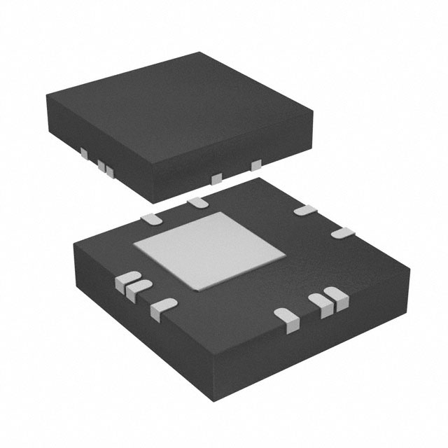
Package Options
The IRS2008 is a high voltage, high speed power
MOSFET and IGBT driver with dependent high and low
side referenced output channels. Proprietary HVIC and
latch immune CMOS technologies enable ruggedized
monolithic construction. The logic input is compatible
with standard CMOS or LSTTL output, down to 3.3 V
logic. The output drivers feature a high pulse current
buffer stage designed for minimum driver crossconduction. The floating channel can be used to drive
an N-channel power MOSFET or IGBT in the high side
configuration which operates up to 200 V. Propagation
delays are matched to simplify the HVIC’s use in high
frequency applications.
16-Lead MLPQ 4x4
(without 2 leads)
8-Lead SOIC
Typical Applications
Base Part Number
IRS2008S
IRS2008M
1
Appliance motor drives, Stepper motor, Servo drives
Micro inverter drives
General purpose three phase inverters
Light electric vehicles (e-bikes, e-scooters, e-toys)
Wireless Charging
General battery driven applications
Standard Pack
Package Type
Form
Quantity
Tape and Reel
2500
Tube/Bulk
95
Tape and Reel
3000
Orderable Part Number
IRS2008STRPBF
8-Lead SOIC
14-Lead MLPQ 4x4
www.infineon.com/gdHalfBridge
IRS2008SPBF
IRS2008MTRPBF
April, 23, 2020
�IRS2008(S,M)PBF
Typical Connection Diagram
(Refer to Lead Assignments for correct pin configuration). This diagram shows electrical connections only. Please refer tour
Application Notes & DesignTips for proper circuit board layout.
2
www.infineon.com/gdHalfBridge
April 23, 2020
�IRS2008(S,M)PBF
Absolute Maximum Ratings
Absolute maximum ratings indicate sustained limits beyond which damage to the device may occur. All voltage parameters are
absolute voltages referenced to COM unless otherwise stated in the table. The thermal resistance and power dissipation ratings
are measured under board mounted and still air conditions.
Symbol
Definition
Min.
Max.
VCC
Low side supply voltage
-0.3
25†
VIN
COM - 0.3
VCC + 0.3
VB
Logic input voltage (IN & SD)
High-side floating well supply voltage
-0.3
225
VS
High-side floating well supply return voltage
VB- 25
VB + 0.3
VHO
Floating gate drive output voltage
VS - 0.3
VB + 0.3
VLO
Low-side output voltage
COM - 0.3
VCC + 0.3
VCC - 25
VCC + 0.3
COM
Power ground
dVS/dt
Allowable VS offset supply transient relative to COM
PD
RthJA
—
50
Package power
dissipation @ TA +25ºC
8-Lead SOIC
—
0.625
14-Lead MLPQ 4x4
—
2.08
Thermal resistance,
junction to ambient
8-Lead SOIC
—
200
14-Lead MLPQ 4x4
—
36
TJ
Junction temperature
—
150
TS
Storage temperature
-55
150
TL
Lead temperature (soldering, 10 seconds)
—
300
†
Units
V
V/ns
W
ºC/W
ºC
All supplies are tested at 25V.
Recommended Operating Conditions
For proper operation, the device should be used within the recommended conditions. All voltage parameters are absolute voltages
referenced to COM unless otherwise stated in the table. The offset rating is tested with supplies of (V CC - COM) = (VB - VS) = 15V.
Symbol
Min
Max
VCC
Low-side supply voltage
10
20
VIN
Logic input voltage(IN & SD)
High-side floating well supply voltage
0
VCC
VB
Definition
VS
High-side floating well supply offset voltage
VHO
Floating gate drive output voltage
VLO
Low-side output voltage
TA
Ambient temperature
†
VS + 10
†
COM - 8
Vs
VS + 20
†
200
Units
V
VB
COM
VCC
-40
125
ºC
Logic operation for VS of –8 V to 200 V. Logic state held for VS of –8 V to –VBS. Please refer to Design Tip DT973 for more details.
3
www.infineon.com/gdHalfBridge
April 23, 2020
�IRS2008(S,M)PBF
Static Electrical Characteristics
(VCC - COM) = (VB - VS) = 15V. TA = 25°C unless otherwise specified. The VIN and IIN parameters are referenced to COM. The VO
and IO parameters are referenced to respective VS and COM and are applicable to the respective output leads HO or LO. The
VCCUV parameters are referenced to COM. The VBSUV parameters are referenced to VS.
Symbol
Min.
Typ.
Max.
VBSUV+
Definition
VBS supply undervoltage positive going threshold
8.0
8.9
9.8
VBSUV-
VBS supply undervoltage negative going threshold
7.4
8.2
9
VBSUVHY
VBS supply undervoltage hysteresis
—
0.7
—
VCCUV+
VCC supply undervoltage positive going threshold
VCC supply undervoltage negative going
threshold
VCC supply undervoltage hysteresis
8.0
8.9
9.8
7.4
8.2
9
—
0.7
—
VCCUVVCCUVHY
ILK
High-side floating well offset supply leakage
—
—
50
IQBS
Quiescent VBS supply current
—
45
75
IQCC
Quiescent VCC supply current
—
300
520
VOH
High level output voltage drop, VBIAS-VO
—
0.05
0.2
VOL
Low level output voltage drop, VO
—
0.02
0.1
Io+
Output high short circuit pulsed current
200
290
—
Io-
Output low short circuit pulsed current
420
600
—
VIH
Logic “1” (HO) & Logic “0” (LO) input voltage
2.5
—
—
VIL
Logic “0” (HO) & Logic “1” (LO) input voltage
—
—
0.8
VSD,TH+
SD input positive going threshold
2.5
—
—
VSD,TH-
SD input negative going threshold
—
—
0.8
Logic “1” Input bias current
—
3
10
Logic “0” Input bias current
—
IIN+
IIN-
—
Units
Test Conditions
V
VB = VS = 200V
µA
All inputs are in the
off state
V
IO = 2 mA
mA
VO = 0V
PW ≤ 10µs
VO = 15V
PW ≤ 10µs
V
Vcc=10V to 20V
µA
5
VIN = 5V
VIN = 0V
Dynamic Electrical Characteristics
VCC = VB = 15V, VS = COM, TA = 25oC, and CL = 1000pF unless otherwise specified.
Symbol
Min.
Typ.
tON
Turn-on propagation delay
—
680
870
tOFF
Turn-off propagation delay
—
150
220
tSD
Shutdown propagation delay
—
160
220
tR
Turn-on rise time
—
70
170
tF
—
30
90
400
520
650
MT
Turn-off fall time
Deadtime, LS turn-off to HS turn-on & HS turn-on
to LS turn-off
Delay matching time (tON, tOFF)
—
—
60
4
www.infineon.com/gdHalfBridge
DT
Definition
Max. Units
Test Conditions
VS = 0V or 200V
ns
VS = 0V
April 23, 2020
�IRS2008(S,M)PBF
Functional Block Diagram
8
VB
7
HO
6
VS
1
Vcc
5
LO
UV
DETECT
R
Pulse
Filter
IN
2
R
Q
S
Pulse
Generator
Dead time
and Short
Through
Prevention
SD
UV
DETECT
Delay
Match
3
4 COM
5
www.infineon.com/gdHalfBridge
April 23, 2020
�IRS2008(S,M)PBF
Lead Definitions
Symbol
Description
Vcc
Low-side and logic supply voltage
VB
High-side gate drive floating supply
VS
High voltage floating supply return
IN
Logic inputs for high and low side gate driver output (HO and LO), in phase with HO
SD
Logic inputs for shutdown
HO
High-side driver output
LO
Low-side driver output
COM
Low-side gate drive return
NC
VB
14
13
NC 1
12 HO
2
11 VS
VB
HIN
2
7
HO
SD
3
6
VS
COM
4
5
LO
SD 3
COM 4
9
NC
5
6
6
7
8
NC
HIN
LO
8
1
16
NC
VCC
Vcc
Lead Assignments
8-Lead SOIC
16-Lead MLPQ 4x4
(without 2 leads)
IRS2008S
IRS2008M
www.infineon.com/gdHalfBridge
NC
April 23, 2020
�IRS2008(S,M)PBF
Application Information and Additional Details
7
www.infineon.com/gdHalfBridge
April 23, 2020
�IRS2008(S,M)PBF
Figure 6A. Turn-On Time vs. Temperature
Figure 6B. Turn-On Time vs. Supply Voltage
Figure 6C. Turn-On Time vs. Input Voltage
Figure 7A. Turn-Off Time vs. Temperature
Figure 7B. Turn-Off Time vs. Supply Voltage
Figure 7C. Turn-Off Time vs. Input Voltage
8
www.infineon.com/gdHalfBridge
April 23, 2020
�IRS2008(S,M)PBF
Figure 8A. Shutdown Time vs. Temperature
Figure 8B. Shutdown Time vs. Voltage
Figure 9A. Turn-On Rise Time vs. Temperature
Figure 9B. Turn-On Rise Time vs. Voltage
Figure 10A. Turn-Off Fall Time vs. Temperature
Figure 10B. Turn-Off Fall Time vs. Voltage
9
www.infineon.com/gdHalfBridge
April 23, 2020
�IRS2008(S,M)PBF
Figure 11A. Deadtime vs. Temperature
Figure 11B. Deadtime vs. Voltage
Figure 12A. Logic “1” Input Voltage
vs. Temperature
Figure 12B. Logic “1” Input Voltage
vs. Voltage
Figure 13A. Logic “0”(HO) & Logic “1”(LO)
& Active SD Input Voltages vs. Temperature
Figure 13B. Logic “0”(HO) & Logic “1”(LO)
& Active SD Input Voltages vs Supply Voltage
10
www.infineon.com/gdHalfBridge
April 23, 2020
�IRS2008(S,M)PBF
Figure 14A. High Level Output Voltage vs.
Temperature
Figure 14B. High Level Output Voltage
vs. Supply Voltage
Figure 15A. Low Level Output Voltage
vs. Temperature
Figure 15B. Low Level Output Voltage
vs. Supply Voltage
Figure 16A. Offset Supply Current vs. Temperature
Figure 16B. Offset Supply Current vs. Voltage
11
www.infineon.com/gdHalfBridge
April 23, 2020
�IRS2008(S,M)PBF
Figure 17A. VBS Supply Current vs. Temperature
Figure 17B. VBS Supply Current vs. Voltage
Figure 18A. VCC Supply Current vs. Temperature
Figure 18B. VCC Supply Current vs. Voltage
Figure 19A. Logic “1” Input Current vs. Temperature
Figure 19B. Logic “1” Input Current vs. Voltage
12
www.infineon.com/gdHalfBridge
April 23, 2020
�IRS2008(S,M)PBF
Figure 20A. Logic “0” Input Bias Current
Figure 20B. Logic “0” Input Bias Current
Figure 21A. VCC\VBS Undervoltage Threshold(+) vs.
Temperature
Figure 21B. VCC\VBS Undervoltage Threshold(-) vs.
Temperature
Figure 22A. Output Source Current vs. Temperature
Figure 22B. Output Source Current vs. Supply
Current
13
www.infineon.com/gdHalfBridge
April 23, 2020
�IRS2008(S,M)PBF
Figure 23A. Output Sink Current vs. Temperature
Figure 23B. Output Sink Current vs. Supply Voltage
Figure 24A. SD input Positive Going Threshold(+)
vs. Temperature
Figure 24B. SD input Positive Going Threshold(+)
vs. Supply Voltage
Figure 25A. SD input Negative Going Threshold(-)
vs. Temperature
Figure 25A. SD input Negative Going Threshold(-)
vs. Voltage
14
www.infineon.com/gdHalfBridge
April 23, 2020
�IRS2008(S,M)PBF
Package Details: 8-Lead SOIC
15
www.infineon.com/gdHalfBridge
April 23, 2020
�IRS2008(S,M)PBF
Tape and Reel Details: 8-Lead SOIC
LOADED TAPE FEED DIRECTION
A
B
H
D
F
C
NOTE : CONTROLLING
DIMENSION IN MM
E
G
CARRIER TAPE DIMENSION FOR 8SOICN
Metric
Imperial
Code
Min
Max
Min
Max
A
7.90
8.10
0.311
0.318
B
3.90
4.10
0.153
0.161
C
11.70
12.30
0.46
0.484
D
5.45
5.55
0.214
0.218
E
6.30
6.50
0.248
0.255
F
5.10
5.30
0.200
0.208
G
1.50
n/a
0.059
n/a
H
1.50
1.60
0.059
0.062
F
D
C
B
A
E
G
H
REEL DIMENSIONS FOR 8SOICN
Metric
Code
Min
Max
A
329.60
330.25
B
20.95
21.45
C
12.80
13.20
D
1.95
2.45
E
98.00
102.00
F
n/a
18.40
G
14.50
17.10
H
12.40
14.40
16
Imperial
Min
Max
12.976
13.001
0.824
0.844
0.503
0.519
0.767
0.096
3.858
4.015
n/a
0.724
0.570
0.673
0.488
0.566
www.infineon.com/gdHalfBridge
April 23, 2020
�IRS2008(S,M)PBF
Package Details: 14-Lead MLPQ 4x4
17
www.infineon.com/gdHalfBridge
April 23, 2020
�IRS2008(S,M)PBF
Tape and Reel Details: 14-Lead MLPQ 4x4
LOADED TAPE FEED DIRECTION
A
B
H
D
F
C
NOTE : CONTROLLING
DIMENSION IN MM
E
G
CARRIER TAPE DIMENSION FOR MLPQ4x4
Metric
Imperial
Code
Min
Max
Min
Max
A
7.90
8.10
0.311
0.358
B
3.90
4.10
0.153
0.161
C
11.70
12.30
0.461
0.484
D
5.45
5.55
0.215
0.219
E
4.25
4.45
0.168
0.176
F
4.25
4.45
0.168
0.176
G
1.50
n/a
0.069
n/a
H
1.50
1.60
0.069
0.063
F
D
C
B
A
E
G
H
REEL DIMENSIONS FOR MLPQ4x4
Metric
Imperial
Code
Min
Max
Min
Max
A
329.60
330.25
12.976
13.001
B
20.95
21.45
0.824
0.844
C
12.80
13.20
0.503
0.519
D
1.95
2.45
0.767
0.096
E
98.00
102.00
3.858
4.015
F
n/a
18.40
n/a
0.724
G
14.50
17.10
0.570
0.673
H
12.40
14.40
0.488
0.566
18
www.infineon.com/gdHalfBridge
April 23, 2020
�IRS2008(S,M)PBF
Part Marking Information
Part number
S2008S
Date code
YWW ?
Pin 1
Identifier
IR logo
? XXXX
?
MARKING CODE
P
Lead Free Released
Lot Code
(Prod mode –
4 digit SPN code)
Assembly site code
Per SCOP 200-002
Non-Lead Free Released
8-Lead SOIC8
IRS2008SPBF
Pin 1 Identifier
Part number
Assembly site
Code
IR logo
S2008M
?YWW ?
XXXXX
Date code
?
MARKING CODE
P
Lead Free Released
Non-Lead
Free Released
-
Lot Code
(Prod mode – 4
digit SPN code)
14-Lead MLPQ 4x4
IRS2008MPBF
19
www.infineon.com/gdHalfBridge
April 23, 2020
�IRS2008(S,M)PBF
Qualification Information†
Industrial†
Comments: This family of ICs is qualified according to relevant
tests of JEDEC47/22/20. IR’s Consumer qualification level is
granted by extension of the higher Industrial level.
Qualification Level
8 Lead SOIC
Moisture Sensitivity Level
14-Lead MLPQ 4x4
Human Body Model
ESD
Machine Model
IC Latch-Up Test
RoHS Compliant
†
††
MSL2††, 260C
(per IPC/JEDEC J-STD-020)
Class 2
(per JEDEC standard JESD22-A114)
Class A
(per EIA/JEDEC standard EIA/JESD22-A115)
Class I
(per JESD78)
Yes
According to IR Qualification Requirements for IC products.
Higher MSL ratings may be available for the specific package types listed here. Please contact your Infineon sales
representative for further information.
20
www.infineon.com/gdHalfBridge
April 23, 2020
�IRS2008(S,M)PBF
Published by
Infineon Technologies AG
81726 München, Germany
© Infineon Technologies AG 2020
All Rights Reserved.
IMPORTANT NOTICE
The information given in this document shall in no event be regarded as a guarantee of conditions or characteristics
(“Beschaffenheitsgarantie”). With respect to any examples, hints or any typical values stated herein and/or any
information regarding the application of the product, Infineon Technologies hereby disclaims any and all warranties
and liabilities of any kind, including without limitation warranties of non-infringement of intellectual property rights of
any third party.
In addition, any information given in this document is subject to customer’s compliance with its obligations stated in
this document and any applicable legal requirements, norms and standards concerning customer’s products and
any use of the product of Infineon Technologies in customer’s applications.
The data contained in this document is exclusively intended for technically trained staff. It is the responsibility of
customer’s technical departments to evaluate the suitability of the product for the intended application and the
completeness of the product information given in this document with respect to such application.
For further information on the product, technology, delivery terms and conditions and prices please contact your
nearest Infineon Technologies office (www.infineon.com).
WARNINGS
Due to technical requirements products may contain dangerous substances. For information on the types in
question please contact your nearest Infineon Technologies office.
Except as otherwise explicitly approved by Infineon Technologies in a written document signed by authorized
representatives of Infineon Technologies, Infineon Technologies’ products may not be used in any applications
where a failure of the product or any consequences of the use thereof can reasonably be expected to result in
personal injury.
21
www.infineon.com/gdHalfBridge
April 23, 2020
�