February 8, 2012
IRS2113MPBF
HIGH- AND LOW-SIDE DRIVER
Features
•
•
•
•
•
•
•
•
•
•
•
•
•
Floating channel designed for bootstrap operation
Fully operational to +600 V
Tolerant to negative transient voltage – dV/dt
immune
Gate drive supply range from 10 V to 20 V
Undervoltage lockout for both channels
3.3 V input logic compatible
Separate logic supply range from 3.3 V to 20 V
Logic and power ground ±5 V offset
CMOS Schmitt-triggered inputs with pull-down
Cycle by cycle edge-triggered shutdown logic
Matched propagation delay for both channels
Output in phase with inputs
Leadfree, RoHS Compliant
Product Summary
Topology
2 channels
VOFFSET
600 V max
VOUT
10 V – 20 V
Io+ & I o- (typical)
2.5 A / 2.5 A
tON & tOFF (typical)
Delay Matching
130 ns & 120 ns
20 ns max
Package Option
Description
The IRS2113MPBF is a high voltage, high speed power
MOSFET and IGBT drivers with independent high and
low side referenced output channels. Proprietary HVIC
and latch immune CMOS technologies enable
ruggedized monolithic construction. The logic input is
compatible with standard CMOS or LSTTL output,
down to 3.3 V logic. The output drivers feature a high
pulse current buffer stage designed for minimum driver
cross-conduction. Propagation delays are matched to
simplify use in high frequency applications. The floating
channel can be used to drive an N-channel power
MOSFET or IGBT in the high side configuration which
operates up to 600 V.
MLPQ4x4-16-Lead
(without 2 leads)
Typical Connection Diagram
(Refer to Leads Assignment for correct pin configurations) This diagram shows electrical connections only.
Please refer to our Application Notes and Design Tips for proper circuit board layout.
www.irf.com
© 2008 International Rectifier
�IRS2113MPBF
†
Qualification Information
††
Qualification Level
Moisture Sensitivity Level
Machine Model
ESD
Human Body Model
Charged Device Model
IC Latch-Up Test
RoHS Compliant
Industrial
(per JEDEC JESD 47)
Comments: This IC has passed JEDEC’s Industrial
qualification. IR’s Consumer qualification level is
granted by extension of the higher Industrial level.
†††
MSL2
MLPQ4x4 14L
(per IPC/JEDEC J-STD020)
Class A (+/-200V)
(per JEDEC standard JESD22-A115)
Class 1B (+/-1000V)
(per EIA/JEDEC standard EIA/JESD22-A114)
Class III (+/-1000V)
(per JEDEC standard JESD22-C101)
Class II, Level A
(per JESD78A)
Yes
†
††
Qualification standards can be found at International Rectifier’s web site http://www.irf.com/
Higher qualification ratings may be available should the user have such requirements. Please
contact your International Rectifier sales representative for further information.
††† Higher MSL ratings may be available for the specific package types listed here. Please contact
your International Rectifier sales representative for further information.
www.irf.com
© 2012 International Rectifier
2
�IRS2113MPBF
Absolute Maximum Ratings
Absolute Maximum Ratings indicate sustained limits beyond which damage to the device may occur. All
voltage parameters are absolute voltages referenced to COM. The thermal resistance and power
dissipation ratings are measured under board mounted and still air conditions.
Definition
Min.
Max.
Units
Symbol
VB
VS
VHO
VCC
VLO
VDD
VSS
VIN
dVS/dt
High-side floating supply voltage
High-side floating supply offset voltage
High-side floating output voltage
Low-side fixed supply voltage
Low-side output voltage
Logic supply voltage
Logic supply offset voltage
Logic input voltage (HIN, LIN & SD)
Allowable offset supply voltage transient (Fig. 2)
-0.3
625
VB - 20
VS - 0.3
-0.3
-0.3
-0.3
VCC - 20
VSS -0.3
—
VB + 0.3
VB + 0.3
25
VCC + 0.3
VSS + 20 (†)
VCC + 0.3
VDD + 0.3
50
PD
Package power dissipation @ TA ≤ 25°C
—
2.08
RthJA
Thermal resistance, junction to ambient
—
36
TJ
Junction temperature
—
150
TS
Storage temperature
-55
150
TL
Lead temperature (soldering, 10 seconds)
—
300
† All supplies are fully tested at 25 V, and an internal 20 V clamp exists for each supply.
V
V/ns
W
°C/W
°C
Recommended Operating Conditions
The input/output logic timing diagram is shown in Figure 1. For proper operation the device should be
used within the recommended conditions. The VS and VSS offset rating are tested with all supplies biased
at 15 V differential.
Symbol
VB
VS
Definition
High-side floating supply absolute voltage
High-side floating supply offset voltage
Min.
VS +10
Max.
VS +20
†
600
VHO
High-side floating output voltage
VS
VB
VCC
Low-side fixed supply voltage
10
20
VLO
Low-side output voltage
0
VCC
VDD
Logic supply voltage
VSS + 3
VSS + 20
VSS
Logic ground offset voltage
5
-5 (††)
VIN
Logic input voltage (HIN, LIN & SD)
VSS
VDD
TA
Ambient temperature
-40
125
† Logic operational for VS of -4 V to +500 V. Logic state held for VS of -4 V to – VBS.
(Please refer to the Design Tip DT97 -3 for more details).
†† When VDD < 5 V, the minimum VSS offset is limited to –VDD.
www.irf.com
Units
V
°C
© 2012 International Rectifier
3
�IRS2113MPBF
Static Electrical Characteristics
VBIAS (VCC, VBS, VDD ) = 15 V, TA = 25°C and VSS = COM unless otherwise specified. The VIL, VTH and IIN
parameters are referenced to VSS and are applicable to all three logic input leads: HIN, LIN and SD. The
VO, and IO parameters are referenced to COM and are applicable to the respective output leads: HO or LO.
Symbol
Definition
Min Typ Max Units
VIH
VIL
VOH
VOL
Logic “1” input voltage
Logic “0” input voltage
High level output voltage, VBIAS - VO
Low level output voltage, VO
9.5
—
—
—
—
—
—
—
—
6.0
1.4
0.15
ILK
Offset supply leakage current
—
—
50
Quiescent VBS supply current
Quiescent VCC supply current
Quiescent VDD supply current
Logic “1” input bias current
Logic “0” input bias current
VBS supply undervoltage positive going threshold
VBS supply undervoltage negative going threshold
VCC supply undervoltage positive going threshold
VCC supply undervoltage negative going threshold
—
—
—
—
—
7.5
7.0
7.4
7.0
125 230
180 340
15 30
20 40
— 5.0
8.6 9.7
8.2 9.4
8.5 9.6
8.2 9.4
Output high short circuit pulsed current
2.0
2.5
IQBS
IQCC
IQDD
IIN+
IINVBSUV+
VBSUVVCCUV+
VCCUVIO+
V
µA
Output low short circuit pulsed current
2.0
2.5
IO = 0 A
IO = 20 mA
VB = VS = 600
V
VIN = 0 V or
VDD
VIN = VDD
VIN = 0 V
V
—
A
IO-
Test
Conditions
—
VO = 0 V,
VIN = VDD
PW ≤ 10 us
VO = 15 V,
VIN = 0 V
PW ≤ 10 us
Dynamic Electrical Characteristics
VBIAS (VCC, VBS, VDD ) = 15 V, CL = 1000 pF, TA = 25°C and VSS = COM unless otherwise specified. The
dynamic electrical characteristics are measured using the test circuit shown in Fig. 3.
Symbol
ton
toff
tsd
tr
tf
MT
Definition
Min Typ Max Units
Turn-on propagation delay
Turn-off propagation delay
Shutdown propagation delay
Turn-on rise time
Turn-off fall time
Delay matching, HS & LS turn on/off
—
—
—
—
—
—
www.irf.com
130 200
120 190
130 160
25 35
17 25
—
20
Test
Conditions
VS = 0 V
VS = 600 V
ns
© 2012 International Rectifier
4
�IRS2113MPBF
Functional Block Diagram
www.irf.com
© 2012 International Rectifier
5
�IRS2113MPBF
Input/Output Pin Equivalent Circuit Diagrams
www.irf.com
© 2012 International Rectifier
6
�IRS2113MPBF
Lead Definitions
PIN
Symbol
Description
1
VDD
Logic supply
2
HIN
Logic input for high-side gate driver output (HO), in phase
3
SD
Logic input for shutdown
4
LIN
Logic input for low-side gate driver output (LO), in phase
5
VSS
Logic ground
6
LO
Low-side gate drive output
7
COM
Low-side return
8
NC
No Connection
9
VCC
Low-side supply
10
NC
No Connection (pin removed)
11
NC
No Connection
12
VS
High-side floating supply return
13
VB
High-side floating supply
14
HO
High-side gate drive output
15
NC
No Connection (pin removed)
16
NC
No Connection
Lead Assignments
16
2
SD
3
LIN
4
14
13
IRS2113MPBF
1
VDD
HIN
15
16L-MLPQ 4x4 with 2
leads removed
12
VS
11
NC
10
COM
9
5
6
7
VCC
8
= Removed lead
IRS2113MPbF
www.irf.com
© 2012 International Rectifier
7
�IRS2113MPBF
Application Information and Additional Details
Figure 1: Input/Output Timing Diagram
Figure 2: Floating Supply Voltage Transient Test Circuit
VCC = 15 V
10 µF
HIN
SD
LIN
0.1
µF 1
2
9
3
13
12
14
10
µF
0.1
µF
CL
6
HO
LO
4
VB
15 V
VS
( O V to 600V )
10 µF
CL
5
7
Figure 3: Switching Time Test Circuit
www.irf.com
© 2012 International Rectifier
8
�IRS2113MPBF
Figure 4: Switching Time Waveform Definitions
Figure 5: Shutdown Waveform Definitions
Figure 6: Delay Matching Waveform Definitions
www.irf.com
© 2012 International Rectifier
9
�IRS2113MPBF
Parameter Temperature Trends
www.irf.com
© 2012 International Rectifier
10
�IRS2113MPBF
www.irf.com
© 2012 International Rectifier
11
�IRS2113MPBF
www.irf.com
© 2012 International Rectifier
12
�IRS2113MPBF
www.irf.com
© 2012 International Rectifier
13
�IRS2113MPBF
www.irf.com
© 2012 International Rectifier
14
�IRS2113MPBF
www.irf.com
© 2012 International Rectifier
15
�IRS2113MPBF
www.irf.com
© 2012 International Rectifier
16
�IRS2113MPBF
www.irf.com
© 2012 International Rectifier
17
�IRS2113MPBF
www.irf.com
© 2012 International Rectifier
18
�IRS2113MPBF
Package Details: MLPQ 4x4 -16L
www.irf.com
© 2012 International Rectifier
19
�IRS2113MPBF
Tape and Reel Details: MLPQ 4x4
www.irf.com
© 2012 International Rectifier
20
�IRS2113MPBF
Part Marking Information:
Ordering Information
Standard Pack
Base Part Number
IRS2113
Package Type
Complete Part Number
Form
Quantity
Tube/Bulk
92
IRS2113MPBF
Tape and Reel
3,000
IRS2113MTRPBF
MLPQ 4x4-16L
The information provided in this document is believed to be accurate and reliable. However, International Rectifier assumes no
responsibility for the consequences of the use of this information. International Rectifier assumes no responsibility for any
infringement of patents or of other rights of third parties which may result from the use of this information. No license is granted
by implication or otherwise under any patent or patent rights of International Rectifier. The specifications mentioned in this
document are subject to change without notice. This document supersedes and replaces all information previously supplied.
For technical support, please contact IR’s Technical Assistance Center
http://www.irf.com/technical-info/
WORLD HEADQUARTERS:
233 Kansas St., El Segundo, California 90245
Tel: (310) 252-7105
www.irf.com
© 2012 International Rectifier
21
�IRS2113MPBF
Revision History
Date
09/24/09
03/24/2010
08/08/2011
02/08/2012
Comment
Initial conversion from SO package style data sheet
Included qual info page
Update the package details
Update pin assignment drawing
www.irf.com
© 2012 International Rectifier
22
�
很抱歉,暂时无法提供与“IRS2113MPBF”相匹配的价格&库存,您可以联系我们找货
免费人工找货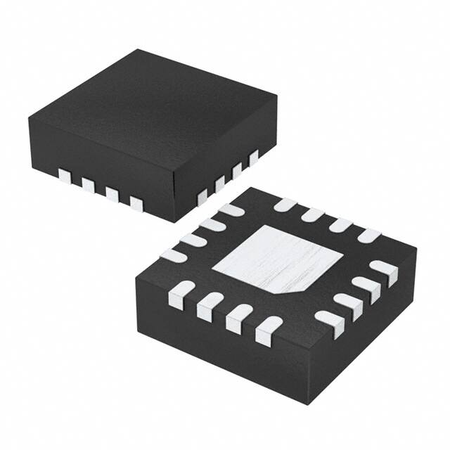


 工商网监
湘ICP备2023018690号
工商网监
湘ICP备2023018690号
