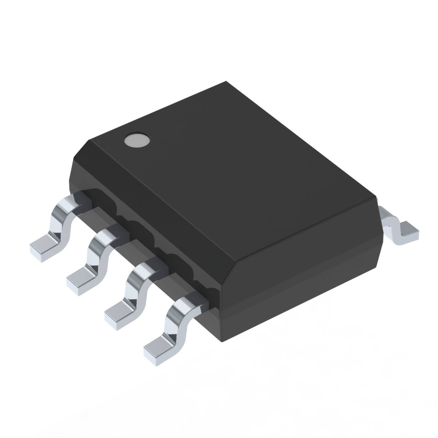
The IRS21171SPBF is not recommended for new designs. For new designs, we recommend IRS2117SPbF or IRS25752LPbF
February 18, 2009
IRS211(7,71,8)(S)
SINGLE CHANNEL DRIVER
Product Summary
IC Features
•
•
•
•
•
•
•
•
•
Floating channel designed for bootstrap
operation
Fully operational to +600V
Tolerant to negative transient voltage, dV/dt
immune
Gate drive supply range from 10 V to 20V
Undervoltage lockout
CMOS Schmitt-triggered inputs with pull-down
Output in phase with input
RoHS compliant
IRS2117 and IRS2118 available in PDIP8
Topology
Single High Side
VOFFSET
600 V
VOUT
10V-20 V
IO+ & IO- (typical)
IN voltage
threshold
290 mA & 600 mA
IRS211(7,8)
9.5 V & 6 V
IRS21171
2.5 V & 0.8 V
Package Type
SOIC8
PDIP8
IRS2117(1)
IRS2118
www.irf.com
© 2008 International Rectifier
1
�The IRS21171SPBF is not recommended for new designs. For new designs, we recommend IRS2117SPbF or IRS25752LPbF
IRS211(7,71,8)(S)
Table of Contents
Page
Description
3
Qualification Information
4
Absolute Maximum Ratings
5
Recommended Operating Conditions
5
Static Electrical Characteristics
6
Dynamic Electrical Characteristics
6
Functional Block Diagram
7
Input/Output Pin Equivalent Circuit Diagram
8
Lead Definitions
9
Lead Assignments
9
Application Information and Additional Details
10
Parameter Temperature Trends
14
Package Details
23
Tape and Reel Details
24
Part Marking Information
25
Ordering Information
26
www.irf.com
© 2008 International Rectifier
2
�The IRS21171SPBF is not recommended for new designs. For new designs, we recommend IRS2117SPbF or IRS25752LPbF
IRS211(7,71,8)(S)
Description
The IRS2117, IRS21171, and IRS2118 are high voltage, high speed power MOSFET and IGBT driver.
Proprietary HVIC and latch immune CMOS technologies enable ruggedized monolithic construction. The
logic input is compatible with standard CMOS outputs. The output driver features a high pulse current buffer
stage designed for minimum cross-conduction. The floating channel can be used to drive an N-channel
power MOSFET or IGBT in the high-side or low-side configuration which operates up to 600 V.
www.irf.com
© 2008 International Rectifier
3
�The IRS21171SPBF is not recommended for new designs. For new designs, we recommend IRS2117SPbF or IRS25752LPbF
IRS211(7,71,8)(S)
†
Qualification Information
Qualification Level
Moisture Sensitivity Level
Machine Model
ESD
Human Body Model
IC Latch-Up Test
RoHS Compliant
Industrial††
(per JEDEC JESD 47)
Comments: This family of ICs has passed JEDEC’s
Industrial qualification. IR’s Consumer qualification level is
granted by extension of the higher Industrial level.
MSL2†††260°C
SOIC8
(per IPC/JEDEC J-STD-020C)
Not applicable
PDIP8
(non-surface mount package style)
Class B
(per JEDEC standard EIA/JESD22-A115)
Class 3A
(per EIA/JEDEC standard JESD22-A114)
Class I, Level A
(per JESD78)
Yes
†
††
Qualification standards can be found at International Rectifier’s web site http://www.irf.com/
Higher qualification ratings may be available should the user have such requirements. Please contact
your International Rectifier sales representative for further information.
††† Higher MSL ratings may be available for the specific package types listed here. Please contact your
International Rectifier sales representative for further information.
www.irf.com
© 2008 International Rectifier
4
�The IRS21171SPBF is not recommended for new designs. For new designs, we recommend IRS2117SPbF or IRS25752LPbF
IRS211(7,71,8)(S)
Absolute Maximum Ratings
Absolute maximum ratings indicate sustained limits beyond which damage to the device may occur. All
voltage parameters are absolute voltages referenced to COM. The thermal resistance and power
dissipation ratings are measured under board mounted and still air conditions.
Symbol
VB
Definition
High-side floating supply voltage
Min.
Max.
-0.3
625
VS
High-side floating supply offset voltage
VB - 25
VHO
High-side floating output voltage
VS - 0.3
VB + 0.3
VB + 0.3
VCC
Logic supply voltage
- 0.3
25
VIN
Logic input voltage
- 0.3
VCC + 0.3
dVS/dt
-----
TJ
Allowable offset supply voltage transient (fig.2)
8 lead SOIC
Package power dissipation @ TA ≤ +25˚C
8 lead PDIP
8 lead SOIC
Thermal Resistance, junction to Ambient
8 lead PDIP
Junction temperature
---
50
0.625
1.0
200
125
150
TS
TL
Storage temperature
Lead Temperature (soldering, 10 seconds)
-55
---
150
300
PD
RθJA
---
Units
V
V/ns
W
ºC/W
ºC
Recommended Operating Conditions
The input/output logic timing diagram is shown in Fig. 1. For proper operation the device should be used
within the recommended conditions. The VS offset rating is tested with all supplies biased at 15 V
differential.
Symbol
VB
Definition
High-Side floating supply absolute voltage
Min.
VS + 10
Max.
VS + 20
†
600
-50 (††)
600
VS
High-side floating supply offset voltage
VST
Transient High side floating supply offset voltage
VHO
High-side floating output voltage
VS
VB
VCC
Logic supply voltage
10
20
VIN
Logic input voltage
0
VCC
TA
Ambient Temperature
-40
125
Units
V
ºC
† Logic operational for VS of -5 V to +600 V. Logic state held for VS of -5 V to – VBS.
†† Operational for transient negative VS of COM - 50 V with a 50 ns pulse width. Guaranteed by design.
Refer to the Application Information section of this datasheet for more details.
www.irf.com
© 2008 International Rectifier
5
�The IRS21171SPBF is not recommended for new designs. For new designs, we recommend IRS2117SPbF or IRS25752LPbF
IRS211(7,71,8)(S)
Dynamic Electrical Characteristics
VBIAS (VCC, VBS) = 15 V, CL = 1000 pF and TA = 25 °C unless otherwise specified.
Symbol
Definition
Min. Typ. Max. Units
IRS21171
--160
230
ton
Turn-on propagation delay
--125
200
IRS211(7,8)
IRS21171
---
160
230
IRS211(7,8)
---
105
180
Turn-on rise time
---
75
130
Turn-off fall time
---
35
65
toff
Turn-off propagation delay
tr
tf
ns
Test Conditions
VS = 0V
VS = 600V
Static Electrical Characteristics
VBIAS (VCC, VBS) = 15 V and TA = 25 °C unless otherwise specified. The VIN, VTH, and IIN parameters
are referenced to COM. The VO and IO parameters are referenced to COM and are applicable to the
respective output leads: HO or LO.
Symbol
VIH
VIL
Definition
Input voltage –logic “1”
Input voltage – logic “0”
Min
Typ
Max
IRS21171
2.5
---
---
IRS211(7,8)
9.5
---
---
IRS21171
---
---
0.8
IRS211(7,8)
6.0
VOH
High level output voltage, VBIAS – VO
---
0.05
0.2
VOL
Low level output voltage, VO
---
0.02
0.1
ILK
Offset supply leakage current
---
---
50
IRS211(7,8)
---
50
240
IRS21171
---
80
150
IRS211(7,8)
---
70
340
IRS21171
---
120
240
---
20
40
IQBS
IQCC
IIN+
IIN-
Quiescent VBS Supply
Current
Quiescent VCC Supply
Current
Logic “1” input bias current
Logic “0” input bias current
IRS2117(1)
IRS2118
IRS2117(1)
Units
V
IO = 2mA
VB = VS = 600V
VIN = 0V or VCC
µA
VIN = VCC
VIN = 0V
IRS2118
---
---
5.0
VBSUV+
VBS supply undervoltage positive going
7.6
8.6
9.6
VBSUV-
VBS supply undervoltage negative going
7.2
8.2
9.2
VCCUV+
VCC supply undervoltage positive going
7.6
8.6
9.6
VCCUV-
VCC supply undervoltage negative going
7.2
8.2
9.2
200
290
VIN = VCC
V
--IO+
Output high short circuit pulsed current
--IO-
Test Conditions
Output low short circuit pulsed current
420
www.irf.com
600
mA
VO = 0V
VIN Logic “1”
PW ≤ 10 µs
VO = 15V
VIN Logic “0”
PW ≤ 10 µs
© 2008 International Rectifier
6
�The IRS21171SPBF is not recommended for new designs. For new designs, we recommend IRS2117SPbF or IRS25752LPbF
IRS211(7,71,8)(S)
Functional Block Diagram
IRS2117(1)
IRS2118
www.irf.com
© 2008 International Rectifier
7
�The IRS21171SPBF is not recommended for new designs. For new designs, we recommend IRS2117SPbF or IRS25752LPbF
IRS211(7,71,8)(S)
I/O Pin Equivalent Circuit Diagrams: IRS211(7,71,8)
IRS2118
IRS2117(1)
www.irf.com
© 2008 International Rectifier
8
�The IRS21171SPBF is not recommended for new designs. For new designs, we recommend IRS2117SPbF or IRS25752LPbF
IRS211(7,71,8)(S)
Lead Definitions
Pin #
1
2
3
4
Symbol
VCC
Description
Logic and gate drive supply
IN
IRS2117(1) Logic input for gate driver output (HO), in phase with HO
IN
NC
IRS2118
Logic input for gate driver output (HO), out of phase with HO
IRS21171 No Connect
COM
IRS2117 / IRS2118 Logic ground
NC
IRS2117 / IRS2118 No Connect
COM
IRS21171 Logic ground
5
NC
No Connect
6
VS
High-side floating supply return
7
HO
High-side gate drive output
8
VB
High-side floating supply
Lead Assignments
COM
IRS21171 SOIC 8
IRS2117 PDIP 8
IRS2117 SOIC 8
IRS2118 PDIP 8
IRS2118 SOIC 8
www.irf.com
© 2008 International Rectifier
9
�The IRS21171SPBF is not recommended for new designs. For new designs, we recommend IRS2117SPbF or IRS25752LPbF
IRS211(7,71,8)(S)
Application Information and Additional Details
HV = 10 to 600V
VCC = 15V
10KF6
0.1 uF
IRS2118
+
100 uF
200 uH
10 uF
1
8
10KF6
0.1 uF
6
7
2
HO
dVS/dt < 50V/ns
10KF6
IRS2117(1)
IRS21171
OUTPUT
MONITOR
IRF820
3
Figure 1 Input/Output Timing Diagram
circuit
Figure 2 Floating Supply Voltage Transient Test
VCC = 15V
IRS2118
0.1 uF
VB
10 uF
1
8
0.1 uF
6
IN
7
2
CL
10 uF
+
10 uF 15V
VS
HO
(0 to
600V)
IRS21171
IRS2117(1)
3
Figure 3 Switching Time Test Circuit
Figure 4 Switching Time Waveform Definition
www.irf.com
© 2008 International Rectifier
10
�The IRS21171SPBF is not recommended for new designs. For new designs, we recommend IRS2117SPbF or IRS25752LPbF
IRS211(7,71,8)(S)
Tolerant to Negative VS Transients
A common problem in today’s high-power switching converters is the transient response of the switch node’s
voltage as the power switches transition on and off quickly while carrying a large current. A typical half bridge
circuit is shown in Figure 5; here we define the power switches and diodes of the inverter.
If the high-side switch (e.g., Q1 in Figures 6 and 7) switches off, while the current is flowing to a load, a current
commutation occurs from high-side switch (Q1) to the diode (D2) in parallel with the low-side switch of the
inverter. At the same instance, the voltage node VS swings from the positive DC bus voltage to the negative
DC bus voltage.
DC+ BUS
Q1
D1
Input
Voltage
To
Load
VS
Q2
D2
DC- BUS
Figure 5: Half Bridge Circuit
DC+ BUS
Q1
OFF
D1
VS
IL
Q2
OFF
D2
DC- BUS
Figure 6: Q1 conducting
Figure 7: D2 conducting
Also when the current flows from the load back to the inverter (see Figures 8 and 9), and Q2 switches on, the
current commutation occurs from D1 to Q2. At the same instance, the voltage node VS swings from the positive
DC bus voltage to the negative DC bus voltage.
www.irf.com
© 2008 International Rectifier
11
�The IRS21171SPBF is not recommended for new designs. For new designs, we recommend IRS2117SPbF or IRS25752LPbF
IRS211(7,71,8)(S)
DC+ BUS
Q1
OFF
DC+ BUS
Q1
OFF
D1
D1
IL
VS
VS
IL
Q2
OFF
Q2
ON
D2
DC- BUS
DC- BUS
Figure 8: D1 conducting
Figure 9: Q2 conducting
However, in a real inverter circuit, the VS voltage swing does not stop at the level of the negative DC bus,
rather it swings below the level of the negative DC bus. This undershoot voltage is called “negative VS
transient”.
The circuit shown in Figure 10 depicts a half bridge circuit with parasitic elements shown; Figures 11 and 12
show a simplified illustration of the commutation of the current between Q1 and D2. The parasitic inductances
in the power circuit from the die bonding to the PCB tracks are lumped together in LD and LS for each switch.
When the high-side switch is on, VS is below the DC+ voltage by the voltage drops associated with the power
switch and the parasitic elements of the circuit. When the high-side power switch turns off, the load current can
momentarily flow in the low-side freewheeling diode due to the inductive load connected to VS (the load is not
shown in these figures). This current flows from the DC- bus (which is connected to the COM pin of the HVIC)
to the load and a negative voltage between VS and the DC- Bus is induced (i.e., the COM pin of the HVIC is at
a higher potential than the VS pin).
DC+ BUS
Q1
OFF
VS
D1
+
_
VLD2
Q2
OFF
IL
D2
+
_
VLS2
DC- BUS
Figure 10: Parasitic Elements
Figure 11: VS positive
Figure 12: VS negative
In a typical power circuit, dV/dt is typically designed to be in the range of 1-5 V/ns. The negative VS transient
voltage can exceed this range during some events such as short circuit and over-current shutdown, when di/dt
is greater than in normal operation.
International Rectifier’s HVICs have been designed for the robustness required in many of today’s demanding
applications. An indication of the IRS211(7,71,8)’s robustness can be seen in Figure 13, where there is
represented the IRS211(7,71,8) Safe Operating Area at VBS=15V based on repetitive negative VS spikes. A
negative VS transient voltage falling in the grey area (outside SOA) may lead to IC permanent damage;
viceversa unwanted functional anomalies or permanent damage to the IC do not appear if negative Vs
transients fall inside SOA.
www.irf.com
© 2008 International Rectifier
12
�The IRS21171SPBF is not recommended for new designs. For new designs, we recommend IRS2117SPbF or IRS25752LPbF
IRS211(7,71,8)(S)
Figure 13: Negative VS transient SOA for IRS211(7,71,8) @ VBS=15V
Even though the IRS211(7,71,8) has shown the ability to handle these large negative VS transient conditions,
it is highly recommended that the circuit designer always limit the negative VS transients as much as possible
by careful PCB layout and component use.
www.irf.com
© 2008 International Rectifier
13
�The IRS21171SPBF is not recommended for new designs. For new designs, we recommend IRS2117SPbF or IRS25752LPbF
IRS211(7,71,8)(S)
Parameter Temperature Trends - 211(7,71,8)
500
Turn-On Rise Time (ns)
Turn-On Rise Time (ns)
500
400
300
200
Max.
100
0
-50
Typ.
400
300
200
Max.
100
Typ.
0
-25
0
25
50
75
100
125
10
12
Temperature ( C)
o
Turn-Off Fall Time (ns)
Turn-Off Fall Time (ns)
20
250
200
150
100
Max.
50
0
-50
Typ.
-25
0
25
50
75
100
200
150
100
Max.
50
Typ.
0
125
10
12
Figure 15A. Turn-Off Fall Tim e
vs. Tem perature
High Level Output Voltage (V)
0.4
0.3
Max.
Typ
-25
0
25
50
75
16
18
20
Figure 15B. Turn-Off Fall Tim e
vs. Supply Voltage
0.5
0.0
-50
14
V BIAS Supply Voltage (V)
Temperature ( C)
o
High Level Output Voltage (V)
18
Figure 14B. Turn-On Rise Tim e
vs. Supply Voltage
250
0.1
16
V BIAS Supply Voltage (V)
Figure 14A. Turn-On Rise Tim e
vs.Tem perature
0.2
14
100
125
0.5
0.4
0.3
Max.
0.2
0.1
Typ
0
10
Temperature ( oC)
12
14
16
18
20
V cc Supply Voltage (V)
Figure 16A. High Level Output
vs. Tem perature (Io = 2m A)
Figure 16B. High Level Output
vs. Supply Voltage (Io = 2m A)
www.irf.com
© 2008 International Rectifier
14
�The IRS21171SPBF is not recommended for new designs. For new designs, we recommend IRS2117SPbF or IRS25752LPbF
0.5
0.4
0.3
0.2
Max.
0.1
0
-50
0.5
Low Level Output Voltage (V)
Low Level Output Voltage (V)
IRS211(7,71,8)(S)
-25
0
25
50
75
100
0.4
0.3
0.2
Max.
0.1
0
125
10
12
Temperature ( oC)
Offset Supply Leakage Current (μA)
Offset Supply Leakage Current (μA)
400
300
200
100
Max.
0
25
50
75
100
125
Temperature ( oC)
400
300
200
100
Logic "1" Input Current (μΑ)
Logic "1" Input Current (μΑ)
100
80
60
40
Max.
20
Typ.
0
0
25
50
75
100
Max.
0
0
100
200
300
400
500
600
V B Boost Voltage (V)
Figure 18B.Offset Supply Leakage
Current vs. VB Boost Voltage
120
-25
20
500
Figure 18A. Offset Supply Leakage
Current vs. Tem perature
- 50
18
Figure 17B. Low Level Output
vs. Supply Voltage
500
-25
16
V cc Supply Voltage (V)
Figure 17A. Low Level Output
vs.Tem perature
0
-50
14
120
100
80
60
40
Max.
Typ.
20
0
10
125
12
14
16
18
20
V cc Supply Voltage (V)
Temperature ( oC)
Figure 19B. Logic "1" (2118 "0") Input Current
vs. Supply Voltage
Figure 19A. Logic "1" (2118 "0") Inp Current
vs. Tem perature
www.irf.com
© 2008 International Rectifier
15
�The IRS21171SPBF is not recommended for new designs. For new designs, we recommend IRS2117SPbF or IRS25752LPbF
IRS211(7,71,8)(S)
Logic "0" Input Current (μΑ)
Logic "0" Input Current (μΑ)
6
Max.
5
4
3
2
1
0
-50
-25
0
25
50
75
100
125
6
Max.
5
4
3
2
1
0
10
12
Temperature ( C)
o
V cc Supply Current (μΑ)
V cc Supply Current (μΑ)
12
Max.
10
Typ.
Mi n.
6
-50
-25
0
25
50
75
100
14
12
10
8
Max.
Typ.
Mi n.
6
-50
125
-25
0
Temperature ( C)
o
V Supply Current (μΑ)
14
12
Max.
Typ.
8
Mi n.
6
0
25
50
50
75
100
125
Figure 22. V cc Undervoltage Threshold (-) vs.
Tem perature
16
-25
25
Temperature ( oC)
Figure 21. V cc Undervoltage Threshold (+)
vs. Tem perature
V BS Supply Current (μΑ)
20
16
14
-50
18
Figure 20B. Logic "0" (2118"1") Input Current
vs. Supply Voltage
16
10
16
V cc Supply Voltage (V)
Figure 20A. Logic "0" (2118 "1") Input Current
vs. Tem perature
8
14
75
100
125
16
14
12
10
8
Max.
Ty
6 Mi
-50 -25
0
25
50
75
100
125
Temperature ( C)
o
Temperature ( C)
o
Figure 23. V BS Undervoltage Threshold (+)
vs. Tem perature
Figure 24. VBS Undervoltage Threshold (-)
vs. Tem perature
www.irf.com
© 2008 International Rectifier
16
�The IRS21171SPBF is not recommended for new designs. For new designs, we recommend IRS2117SPbF or IRS25752LPbF
500
400
Output Source Current (mA)
Output Source Current (mA)
IRS211(7,71,8)(S)
Typ.
300
200
Min.
100
0
-50
-25
0
25
50
75
100
500
400
300
200
Typ.
100
Min.
0
10
125
12
Figure 25A. Output Source Current
vs. Tem perature
Output Sink Current (mA)
Output Sink Current (mA)
800
Typ.
Min.
400
200
-25
0
25
50
75
20
1000
800
600
Typ.
400
200
Min.
0
10
100 125
12
14
16
18
20
V BIAS Supply Voltage (V)
Temperature ( oC)
Figure 26B. Output Sink Current
vs. Supply Voltage
Figure 26A. Output Sink Current
vs.Tem perature
vs Offset Supply Voltage (V)
18
Figure 25B. Output Source Current
vs. Supply Voltage
1000
0
-50
16
V BIAS Supply Voltage (V)
Temperature ( oC)
600
14
0
-2
-4
Typ.
-6
-8
-10
-12
10
12
14
16
18
20
V bs Floating Supply Voltage (V)
Figure 27. Maximum VS Negative Offset vs.
Supply Voltage
www.irf.com
© 2008 International Rectifier
17
�The IRS21171SPBF is not recommended for new designs. For new designs, we recommend IRS2117SPbF or IRS25752LPbF
IRS211(7,71,8)(S)
500
Turn-on Delay Time (ns)
Turn-on Delay Time (ns)
Parameter Temperature Trends - 211(7,8)
400
300
200
Max.
100
Typ.
0
-50
-25
0
25
50
75
100
400
300
Max.
200
Typ.
100
0
10
125
12
14
16
18
20
Temperature ( oC)
V BIAS Supply Voltage (V)
Figure 28A. IRS211(7,8) Turn-On Tim e
vs. Tem perature
Figure 28B. IRS211(7,8) Turn-On Tim e
vs. Supply Voltage
500
Turn-Off Time (ns)
500
Turn-Off Time (ns)
500
400
300
200
Max.
100
400
300
Ma
200
Typ.
100
Typ.
0
-50
0
-25
0
25
50
75
100
10
125
12
13
15
12
13
11
10
Mi n.
8
-50
16
18
20
Figure 29B. IRS211(7,8) Turn-Off Tim e
vs. Supply Voltage
Input Voltage (V)
Input Voltage (V)
Figure 29A. IRS211(7,8) Turn-Off Tim e
vs. Tem perature
9
14
V BIAS Supply Voltage (V)
Temperature ( C)
o
11
9
Mi n.
7
5
-25
0
25
50
75
100
125
10
Temperature ( oC)
12
14
16
18
20
Vcc Supply Voltage (V)
Figure 30A. IRS2117 Logic "1" (2118 "0") Input
Voltage vs. Tem perature
Figure 30B. IRS2117 Logic "1" (2118 "0") Input
Voltage vs. Supply Voltage
www.irf.com
© 2008 International Rectifier
18
�The IRS21171SPBF is not recommended for new designs. For new designs, we recommend IRS2117SPbF or IRS25752LPbF
9
15
8
12
Input Voltage (V)
Input Voltage (V)
IRS211(7,71,8)(S)
7
6
Max.
5
4
-50
9
6
Max.
3
0
-25
0
25
50
75
100
125
10
12
Temperatre ( oC)
V Supply Current (μΑ)
V Supply Current (μΑ)
800
600
400
Max.
200
Typ.
25
800
600
400
50
75
100
Max.
200
Typ.
0
10
125
12
1000
18
20
1000
V cc Supply Current (μΑ)
V cc Supply Current (μA)
16
Figure 32B. 211(7,8) V BS Supply
Current
Figure 32A. 211(7,8) V BS Supply Current
vs. Tem perature
800
600
Max.
200
Typ.
0
-50
14
V BS Supply Voltage (V)
Temperature ( C)
o
400
20
1000
0
0
18
V cc Supply Voltage (V)
1000
-25
16
Figure 31B. IRS2117 Logic "0" (2118 "1")
Input Voltage vs. Supply Voltage
Figure 31A. IRS2117 Logic "0" (2118 "1") Input
Voltage vs. Tem perature
-50
14
-25
0
25
50
75
100 125
800
600
400
Max.
200
Typ.
0
10
Temperature ( oC)
12
14
16
18
20
V cc Supply Voltage (V)
Figure 33A. 211(7,8) V cc Supply Current
vs. Tem perature
Figure 33B. 211(7,8) V cc Supply Current
vs. Supply Voltage
www.irf.com
© 2008 International Rectifier
19
�The IRS21171SPBF is not recommended for new designs. For new designs, we recommend IRS2117SPbF or IRS25752LPbF
IRS211(7,71,8)(S)
Parameter Temperature Trends - 21171
500
Turn-on Delay Time (ns)
Turn-on Delay Time (ns)
500
400
300
200
Max.
100
Typ.
0
-50
400
300
Max.
200
Typ.
100
0
-25
0
25
50
75
100
125
10
12
14
Temperature ( C)
500
500
400
400
300
200
Max.
100
Max.
200
Typ.
100
0
-25
0
25
50
75
100
10
125
12
Figure 35A. IRS21171 Turn-Off Tim e
vs. Tem perature
16
18
20
Figure 35B. IRS21171 Turn-Off Tim e
vs. Supply Voltage
5
5
4
4
Input Voltage (V)
Input Voltage (V)
14
V BIAS Supply Voltage (V)
Temperature ( oC)
3
1
-50
20
300
Typ.
2
18
Figure 34B. IRS21171 Turn-On Tim e
vs. Supply Voltage
Turn-Off Time (ns)
Turn-Off Time (ns)
Figure 34A. IRS21171 Turn-On Tim e
vs. Tem perature
0
-50
16
V BIAS Supply Voltage (V)
o
Mi n.
3
2
Min.
1
-25
0
25
50
75
100
10
125
12
14
16
18
20
Vcc Supply Voltage (V)
Temperature ( C)
o
Figure 36B. IRS21171 Logic "1" Input Voltage
vs. Supply Voltage
Figure 36A. IRS21171 Logic "1" Input Voltage
vs. Tem perature
www.irf.com
© 2008 International Rectifier
20
�The IRS21171SPBF is not recommended for new designs. For new designs, we recommend IRS2117SPbF or IRS25752LPbF
IRS211(7,71,8)(S)
5
5
Input Voltage (V)
Input Voltage (V)
4
3
2
Max.
1
4
3
2
Max.
1
0
0
-50
-25
0
25
50
75
100
10
125
12
14
Temperature ( C)
o
20
Figure 37B. IRS21171 Logic "0" Input Voltage
vs. Supply Voltage
400
400
V Supply Current (μΑ)
V Supply Current (μΑ)
18
V cc Supply Voltage (V)
Figure 37A. IRS21171 Logic "0" Input Voltage
vs. Tem perature
300
200
Max.
100
Typ.
-50
300
200
Max.
100
Typ.
0
0
-25
0
25
50
75
100
10
125
12
14
16
18
20
V BS Supply Voltage (V)
Temperature ( C)
o
Figure 38B. IRS21171 V BS Supply Current
vs. Supply Voltage
Figure 38A. IRS21171 V BS Supply Current
vs. Tem perature
500
500
400
V cc Supply Current (μΑ)
V cc Supply Current (μA)
16
300
Max.
200
100
Typ.
0
-50
-25
0
25
50
75
100
400
300
200
Max.
100
Typ.
125
0
10
Temperature ( oC)
12
14
16
18
20
V cc Supply Voltage (V)
Figure 39A. IRS21171 V cc Supply Current
vs. Tem perature
Figure 39B. IRS21171 V cc Supply Current
vs. Supply Voltage
www.irf.com
© 2008 International Rectifier
21
�The IRS21171SPBF is not recommended for new designs. For new designs, we recommend IRS2117SPbF or IRS25752LPbF
IRS211(7,71,8)(S)
Figure 40. IRS2117/IRS2118 TJ
vs. Frequency (IRFBC20)
RGATE=33Ω, VCC=15V
Figure 41. IRS2117/IRS2118 TJ
vs. Frequency (IRFBC30)
RGATE=22Ω, VCC=15V
Figure 42. IRS2117/IRS2118 TJ
vs. Frequency (IRFBC40)
RGATE=15Ω, VCC=15V
Figure 43. IRS2117/IRS2118 TJ
vs. Frequency (IRFPE50)
RGATE=10Ω, VCC=15V
www.irf.com
© 2008 International Rectifier
22
�The IRS21171SPBF is not recommended for new designs. For new designs, we recommend IRS2117SPbF or IRS25752LPbF
IRS211(7,71,8)(S)
Package Details
www.irf.com
© 2008 International Rectifier
23
�The IRS21171SPBF is not recommended for new designs. For new designs, we recommend IRS2117SPbF or IRS25752LPbF
IRS211(7,71,8)(S)
Package Details: SOIC8N, Tape and Reel
LOADED TAPE FEED DIRECTION
A
B
H
D
F
C
NOTE : CONTROLLING
DIM ENSION IN M M
E
G
CARRIER TAPE DIMENSION FOR
Metric
Code
Min
Max
A
7.90
8.10
B
3.90
4.10
C
11.70
12.30
D
5.45
5.55
E
6.30
6.50
F
5.10
5.30
G
1.50
n/a
H
1.50
1.60
8SOICN
Imperial
Min
Max
0.311
0.318
0.153
0.161
0.46
0.484
0.214
0.218
0.248
0.255
0.200
0.208
0.059
n/a
0.059
0.062
F
D
C
B
A
E
G
H
REEL DIMENSIONS FOR 8SOICN
Metric
Code
Min
Max
A
329.60
330.25
B
20.95
21.45
C
12.80
13.20
D
1.95
2.45
E
98.00
102.00
F
n/a
18.40
G
14.50
17.10
H
12.40
14.40
www.irf.com
Imperial
Min
Max
12.976
13.001
0.824
0.844
0.503
0.519
0.767
0.096
3.858
4.015
n/a
0.724
0.570
0.673
0.488
0.566
© 2008 International Rectifier
24
�The IRS21171SPBF is not recommended for new designs. For new designs, we recommend IRS2117SPbF or IRS25752LPbF
IRS211(7,71,8)(S)
Part Marking Information
Part number
IRSxxxxx
Date code
YWW ?
Pin 1
Identifier
?
MARKING CODE
P
Lead Free Released
IR logo
? XXXX
Lot Code
(Prod mode –
4 digit SPN code)
Assembly site code
Per SCOP 200-002
Non-Lead Free Released
www.irf.com
© 2008 International Rectifier
25
�The IRS21171SPBF is not recommended for new designs. For new designs, we recommend IRS2117SPbF or IRS25752LPbF
IRS211(7,71,8)(S)
Ordering Information
Base Part Number
IRS2117
Package Type
SOIC8N
PDIP8
IRS21171
SOIC8N
SOIC8N
IRS2118
PDIP8
Standard Pack
Complete Part Number
Form
Quantity
Tube/Bulk
95
IRS2117SPBF
Tape and Reel
2500
IRS2117STRPBF
Tube/Bulk
50
IRS2117PBF
Tube/Bulk
95
IRS21171SPBF
Tape and Reel
2500
IRS21171STRPBF
Tube/Bulk
95
IRS2118SPBF
Tape and Reel
2500
IRS2118STRPBF
Tube/Bulk
50
IRS2118PBF
The information provided in this document is believed to be accurate and reliable. However, International Rectifier assumes no
responsibility for the consequences of the use of this information. International Rectifier assumes no responsibility for any infringement
of patents or of other rights of third parties which may result from the use of this information. No license is granted by implication or
otherwise under any patent or patent rights of International Rectifier. The specifications mentioned in this document are subject to
change without notice. This document supersedes and replaces all information previously supplied.
For technical support, please contact IR’s Technical Assistance Center
http://www.irf.com/technical-info/
WORLD HEADQUARTERS:
233 Kansas St., El Segundo, California 90245
Tel: (310) 252-7105
www.irf.com
© 2008 International Rectifier
26
�