Class D Audio
Class D Audio IC
IRS2452AM
Features
•
•
•
•
•
•
•
•
•
Product Summary
2 channel integrated analog input Class D audio
amplifier driver
Differential or single-ended input
Versatile protection control enabling latched, nonlatched, or host controlled shutdown function
Programmable over current protection
Programmable dead-time generation
External thermal sensor input
Click noise reduction
Under voltage protection
High noise immunity
Topology
Half-Bridge/Full-Bridge
VOFFSET (max)
+/- 200 V
IO+ & IO- (typical)
0.5 A & 0.6 A
Selectable deadtime
DC offset
45/65/85/105 ns
60 dB
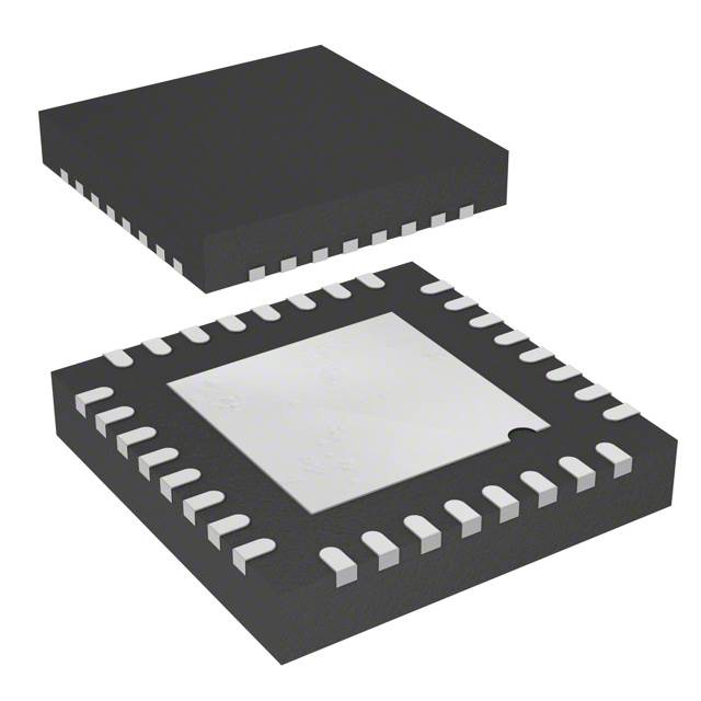
Package Options
MLPQ 7X7mm 32L (0.50 mm pitch)
Ordering Information
Base Part Number
Package Type
IRS2452AM
MLPQ 32 7x7
1
Standard Pack
Form
Quantity
Tape and Reel
3000
Orderable Part Number
IRS2452AM
2016-10-05
�IRS2452AM
Description
The IRS2452AM integrates two channels of high voltage, high performance Class D audio amplifier drivers with
PWM modulators and protections. In conjunction with external MOSFET, the IRS2452AM forms a complete 2
channel Class D audio amplifier. The IRS2452AM is designed with floating analog inputs and protection control
interface pins convenient for half bridge applications. High and low side MOSFET are protected from over current
conditions by a programmable over current protection. Essential elements of PWM modulator section allow
flexible system design. A small MLPQ 7x7mm package enhances the benefit of smaller size of Class D topology.
The IRS2452AM is a lead-free, ROHS compliant.
†
Qualification Information
††
Industrial
Comments: This family of ICs has passed JEDEC’s Industrial
qualification. IR’s Consumer qualification level is granted by
extension of the higher Industrial level.
Qualification Level
Moisture Sensitivity Level
Machine Model
ESD
Human Body Model
Charge Device Model
IC Latch-Up Test
RoHS Compliant
MSL2†††, 260°C
(per IPC/JEDEC J-STD-020)
Class B
(per JEDEC standard EIA/JESD22-A115)
Class 1B
(per EIA/JEDEC standard JESD22-A114)
Class 0B
(per EIA/JEDEC standard JESD22-C101)
Class I, Level A
(per JESD78)
Yes
†
††
Qualification standards can be found at Infineon web site http://www.infineon.com/product-info/reliability/
Higher qualification ratings may be available should the user have such requirements. Please contact your
Infineon Technology sales representative for further information.
††† Higher MSL ratings may be available for the specific package types listed here. Please contact your Infineon
Technology sales representative for further information.
2
Rev. 1.2
2016-10-05
�IRS2452AM
Typical Connection Diagram
R7
R20
R22
C20
D20
+B
R24
R26
A/B
D22
Q60
R28
R30
CLK
C3
C1
INPUT 2
R1
R40
C5
R42
C7
R3
R46
R5
-5V
C64
L61
D40
R44
CH2 OUTPUT
Q62
R49
R60
R47
C68
C9
C10
R6
+5V
IRS20524[ES1]
R48
C40
C70
C72
PTC1
VCC
-B
C2
R2
R50
INPUT 1
POWER GND
Q63
C8
R4
R43
C69
R45
L62
D41
C4
AGND
C6
R31
D23
C11
C21
R8
3
Rev. 1.2
R23
R25
D21
R61
CH1 OUTPUT
R41
BTL
C71
Q61
C65
R29
R27
R21
2016-10-05
�IRS2452AM
Absolute Maximum Ratings
Absolute Maximum Ratings indicate sustained limits beyond which damage to the device may occur. All voltage
parameters are absolute voltages referenced to COM; all currents are defined positive into any lead. The
Thermal Resistance and Power Dissipation ratings are measured under board mounted and still air conditions.
Symbol
VBn
Definition
High side floating supply voltage
††
Min.
Max.
Units
-0.3
415
V
VSn
High side floating supply voltage , n=1-2
VBn -15
VBn +0.3
V
VHon
High side floating output voltage, n=1-2
VSn -0.3
VBn +0.3
V
CSH pin input voltage, n=1-2
VSn -0.3
VBn +0.3
V
-0.3
15.5
V
-0.3
VCC +0.3
V
(See IAAZ)
210
V
-1
(See ISSZ)
VAA +0.3
V
VSS -0.3
VAA +0.3
V
-
±3
mA
VCSHn
VCC
VCC low side fixed supply voltage
VLon
Low side output voltage, n=1-2
††
††
VAA
Floating input positive supply voltage
VSS
Floating input negative supply voltage
VGND
Floating input supply ground voltage
IIN-n
VCSD
††
†
Inverting input current , n=1-2
SD pin input voltage
VGND -0.3
VAA +0.3
V
COMP pin input voltage, n=1-2
VSS -0.3
VAA +0.3
V
VCLK
CLK pin input voltage
VSS -0.3
VAA +0.3
V
VBTL
BTL pin input voltage
VSS -0.3
VAA +0.3
V
VAB
A/B pin input voltage
VSS -0.3
VAA +0.3
V
VCOMPn
VDT
DT pin input voltage
-0.3
VCC +0.3
V
VOTP
OTP pin input voltage
-0.3
VCC +0.3
V
VCSLn
CSL pin input voltage, n=1-2
-0.3
VCC +0.3
V
-
10
mA
-
10
mA
††
IAAZ
Floating input positive supply zener clamp current
ICCZ
Low side VCC supply zener clamp current
IBSZn
††
††
Floating supply zener clamp current , n=1-2
-
10
mA
dVSn/dt
Allowable Vs voltage slew rate, n=1-2
-
50
V/ns
dVSS/dt
Allowable Vss voltage slew rate
-
50
V/ms
4
Rev. 1.2
†††
2016-10-05
�IRS2452AM
Absolute Maximum Ratings (Cont’d)
Symbol
Min.
Max.
Units
-
6
W
Thermal resistance, Junction to ambient
-
20
°C/W
TJ
Junction Temperature
-
150
°C
TS
Storage Temperature
-55
150
°C
TL
Lead temperature (Soldering, 10 seconds)
-
300
°C
Pd
RthJA
†
††
Definition
††††
Maximum power dissipation @ TA ≤ +25°C
††††
IN-1 and IN-2 contain clamping diode to GND.
VAA-VSS, VCC-COM, VB1-VS1 and VB2-VS2 contain internal shunt zener diodes. Note that the
voltage ratings of these can be limited by the clamping current.
For the rising and falling edges of step signal of 10V. VSS=15V to 200V.
According to JESD51-5. JEDEC still air chamber.
†††
††††
5
Rev. 1.2
2016-10-05
�IRS2452AM
Recommended Operating Conditions
For proper operation, the device should be used within the recommended conditions below. The Vs and COM offset ratings
are tested with supplies biased at VAA-VSS=10V, VCC =12V, COM2=COM and VB-VS=12V. All voltage parameters are absolute
voltages referenced to COM; all currents are defined positive into any lead.
Symbol
Definition
Min.
Max.
Units
VSn +10
VSn +14
V
(Note1)
400
V
VSS + 4.5
VSS + 15
V
Floating input positive supply zener clamp current
1
11
mA
VSS
Floating input supply absolute voltage
0
200
V
VHon
High side floating output voltage, n=1-2
Vs
VB
V
VCC
Low side fixed supply voltage
10
14
V
VLon
Low side output voltage, n=1-2
0
VCC
V
(Note2)
VSS
(Note2)
VAA
VBn
High side floating supply absolute voltage, n=1-2
VSn
High side floating supply offset voltage
VAA
Floating input supply voltage
IAAZ
VGND
GND pin input voltage
(Note2)
(Note2)
V
VIN-n
Inverting input voltage, n=1-2
VCSD
CSD pin input voltage
VGND
VAA
V
VCOMPn
COMP pin input voltage, n=1-2
VSS
VAA
V
CCOMPn
COMP pin phase compensation capacitor to GND, n=1-2
2.2
-
nF
VGND -0.5
VGND +0.5
V
VCLK
CLK pin input voltage
VGND
VAA
V
VBTL
BTL pin input voltage
VSS
VAA
V
VAB
A/B pin input voltage
VSS
VAA
V
VDT
DT pin input voltage
0
VCC
V
VOTP
OTP pin input voltage
0
VCC
V
VCSHn
CSH pin input voltage, n=1-2
VSn
VBn
V
VCSLn
CSL pin input voltage, n=1-2
0
VCC
V
-
50
V/ms
dVSS/dt
Allowable VSS voltage slew rate upon power-up
(Note3)
fSW
Switching frequency
-
800
kHz
fCLK
(Note4)
CLK frequency
-
800
kHz
TA
Ambient Temperature
-40
125
°C
(Note 1) Logic operational for Vsn equal to –5V to +400V. Logic state held for Vsn equal to –5V to –VBSn.
(Note 2) GND input voltage is limited by IIN-n.
(Note 3) Vss ramps up from 0V to 200V.
(Note 4) The CLK input frequency needs to be within +/-10% of self-oscillating frequency in order to synchronize PWM in a
typical self-oscillating application.
6
Rev. 1.2
2016-10-05
�IRS2452AM
Electrical Characteristics
VCC= VBS1=VBS2 =VDT=12V, VSS=VS1=VS2=COM =0V, VGND=5V, VAA=VBTL=VAB=10V, CL=1nF and TA=25°C unless otherwise
specified.
Symbol
Definition
Low Side Supply
UVCC+
Vcc supply UVLO positive threshold
UVCCVcc supply UVLO negative
threshold
UVCCHYS
UVCC hysteresis
IQCC
Low side quiescent current
VCLAMPL
Low side zener diode clamp voltage
High Side Floating Supply
High side well UVLO positive
UVBS+n
threshold, n=1-2
High side well UVLO negative
UVBS-n
threshold, n=1-2
UVBSHYSn
UVBS hysteresis, n=1-2
IQBSn
High side quiescent current, n=1-2
High to Low side leakage current,
ILKHn
n=1-2
High side zener diode clamp
VCLAMPHn
voltage, n=1-2
Floating Input Supply
UVAA+
VAA floating supply UVLO positive
threshold from VSS
UVAAVAA floating supply UVLO negative
threshold from VSS
UVAAHYS
UVAA hysteresis
IQAASD
Floating Input positive quiescent
supply current in shutdown mode
IQAA0
Floating Input positive quiescent
supply current, positive input
IQAA1
Floating Input positive quiescent
supply current, negative input
IQAAST
Floating Input positive quiescent
supply current in start-up mode
IQAABTL
Floating Input positive quiescent
supply current, negative input
ILKM
VCLAMPM
7
Floating input side to Low side
leakage current
Floating supply zener diode clamp
voltage
Rev. 1.2
Min
Typ
Max
Units
Test Conditions
8.4
8.2
8.9
8.7
9.4
9.2
V
V
14.7
0.2
15.3
6
16.2
V
mA
V
8.0
8.5
9.0
V
7.8
8.3
8.8
V
-
0.2
-
1
V
mA
-
-
50
µA
VBn=VSn =400V
14.7
15.3
16.2
V
IBSn=5mA
8.2
8.7
9.2
V
GND pin floating
7.7
8.2
8.7
V
GND pin floating
-
0.5
2.5
4
V
mA
GND pin floating
VCSD =VGND
-
8
11
mA
VIN- = VSS+5.2V
-
5
8
mA
VIN- = VSS+4.8V
-
6
8
mA
VCSD = VGND+2.5V
-
5
8
mA
VIN- = VSS+4.8V,
VBTL=GND
-
-
50
µA
14.7
15.3
16.2
V
VAA=VSS=VGND=
100V
IAA=5mA,
VCSD =VGND
VDT=VCC
ICC=5mA
2016-10-05
�IRS2452AM
Electrical Characteristics (Cont’d)
Symbol
Definition
Min
Typ
Max
Units
Test Conditions
Audio Input (GND=0V, VAA=5V, VSS=-5V, COM =VCC =-5V, VS1=VS2=CSH1=CSH2=-5V, DT=-5V)
VOsn
CHn input offset voltage, n=1-2
-18
0
18
mV
IBINn
CHn input bias current, n=1-2
40
nA
GBWn
CHn small signal bandwidth, n=1-2
5
MHz
CCOMPn=2.2nF,
Note 1
Rfn=10k, Note 1
VCOMPn
CHn OTA Output voltage, n=1-2
VAA-1
VSS+1
V
gmn
CHn OTA transconductance, n=1-2
80
200
260
mS
VIN-n=10mV
GVn
CHn OTA gain, n=1-2
60
dB
VNrmsn
CHn OTA input noise voltage, n=1-2
250
mVrms
BW=20kHz,
Resolution BW=22Hz
Fig.5
SRn
CHn slew rate, n=1-2
±5
V/us
CCOMPn=2.2nF
CMRRn CHn common-mode rejection ratio,
dB
60
n=1-2
PSRRn
CHn supply voltage rejection ratio,
dB
65
n=1-2
PWM Comparator
VthPWM
PWM comparator threshold in COMP
(VAA –
V
VSS)/2
fOTAn
CHn COMP pin star-up local
MHz
VCSD =VGND+2.5V
0.6
oscillation frequency, n=1-3
Clock Input (GND=0V, VAA=5V, VSS=-5V, COM =VCC =-5V, VS1=VS2=CSH1=CSH2=-5V, DT=-5V)
VIHCLK
CLK high level input threshold
8
V
VILCLK
CLK low level input threshold
2
V
IIHCLK+
CLK high level input bias current
-35
35
µA
VCLK=VAA
IILCLKCLK low level input bias current
-45
45
µA
VCLK=VSS
VTHAB
AB high level input threshold
0.40x
0.50x
0.60x
V
(VAA(VAA(VAAGND)
GND)
GND)
IIHAB+
AB high level input bias current
-35
35
µA
VAB=VAA
IILABAB high level input bias current
-45
45
µA
VAB=GND
BTL Mode (GND=0V, VAA=5V, VSS=-5V, COM =VCC =-5V, VS1=VS2=CSH1=CSH2=-5V, DT=-5V)
VTHBTL
BTL high level input threshold
0.40x
0.50x
0.60x
V
(VAA(VAA(VAAGND)
GND)
GND)
IIHBTL+
BTL high level input bias current
-35
35
µA
VBTL=VAA
IILBTLBTL high level input bias current
-45
45
µA
VBTL=GND
8
Rev. 1.2
2016-10-05
�IRS2452AM
Electrical Characteristics (Cont’d)
Symbol
Definition
Min
Typ
Max
Protection
VthOCLn
CHn low side OC threshold in VCSLn,
1.1
1.2
1.3
n=1-2
VthOCHn
CHn high side OC threshold in VCSHn, 1.1+ Vs 1.2+ Vs
1.3+ Vs
n=1-2
Vth1
CSD pin shutdown release threshold 0.52xVAA-GND 0.68xVAA-GND 0.84xVAA-GND
0.26xVAA-GND 0.30xVAA-GND 0.34xVAA-GND
Vth2
CSD pin self reset threshold
ICSD+
CSD pin discharge current
70
100
130
ICSDCSD pin charge current
70
100
130
tSSDn
CHn shutdown propagation delay
from VCSD < VGND+ Vth1 to Shutdown,
140
250
n=1-2
tOCHn
CHn propagation delay time from
400
500
VCSHn > VthOCHn to Shutdown, n=1-2
tOCLn
CHn propagation delay time from
270
350
Vsn> VthOCL to Shutdown, n=1-2
VOTP
OTP pin input threshold
2.8
IOTP
OTP bias sourcing current
0.6
-
9
Rev. 1.2
Units
Test Conditions
V
V
V
V
µA
µA
ns
Vs=400V
VCSD = VGND + 2.4V
VCSD = VGND + 2.4V
ns
ns
V
mA
OTPn=0V
2016-10-05
�IRS2452AM
Electrical Characteristics (Cont’d)
Symbol
Definition
Min
Typ
Max
Units
Test Conditions
CHn output high short circuit current
(Source) , n=1-2
CHn output low short circuit current
(Sink) , n=1-2
-
0.5
-
A
-
0.6
-
A
Vo=0V, PWVDT> VDT2,
VDTM=COM
ns
VDT2>VDT> VDT3,
VDTM=COM
ns
VDT VthOCL to Shutdown Waveform
11
Rev. 1.2
2016-10-05
�IRS2452AM
VthOCH
CSH
VS
90%
HO
tOCH
Figure 4 VCSH > VthOCH to Shutdown Waveform
12
Rev. 1.2
2016-10-05
�IRS2452AM
Waveform Definitions (Cont’d)
DUT
10 Ω
5V
10 µF
VAA
GND
3.3 µF 100 Ω
47 kΩ
5V
OTA
INCOMP
2nF
10 µF
10 Ω
VSS
100 Ω
10 Ω
10 µF
100 kΩ
LT1028
100 Ω
`
NOISE OUT
47 µF
10 µF
10 Ω
GND
100 Ω
10 kΩ
10 nF
Figure 5: OTA input noise voltage mesurent circuit
13
Rev. 1.2
2016-10-05
�IRS2452AM
VB1
CSH1
DT
CSD
Functional Block Diagram
OCH1
PWM
1
GG
IN-1
OTA1
COMP1
DT1
HO1
VS1
IN+1
DT
VSS
GG
GG
PROT
CTRL
BTL
PWM
2
2CH
VS2
GG
CH1_CLK
CH2_CLK
VB2
CSH2
BTL
Rev. 1.2
HO2
OCH2
OTP
CLK
A/B
14
CSL2
OCL2
DT2
COMP2
CLK
LO1
COM
LO2
OTA2
IN-2
VCC
SD
VAA
IN+2
CSL1
OCL1
GND
2016-10-05
�IRS2452AM
Input/Output Pin Equivalent Circuit Diagrams
VAA
ESD
Diode
CHARGE
VAA
IN-
ESD
Diode
15V
Zener
Diode
IN+
CSD
ESD
Diode
ESD
Diode
200 V
GND
VSS
DISCHARGE
VSS
COM
VCC
VAA
ESD
Diode
ESD
Diode
OTP
COMP, BTL, CLK, A/B
ESD
Diode
ESD
Diode
VSS
15
Rev. 1.2
VREF
COM
2016-10-05
�IRS2452AM
Input/Output Pin Equivalent Circuit Diagrams (Cont’d)
VB
15 V
Clamp
ESD
Diode
HO, CSH
ESD
Diode
VS
400 V
V CC
VCC
20 V
Clamp
ESD
Diode
LO, CSL
ESD
Diode
COM
16
Rev. 1.2
2016-10-05
�IRS2452AM
Lead Definitions
Description
Pin #
Symbol
I/O
1
2
3
4
5
6
7
8
9
10
11
12
13
14
15
16
17
18
19
20
21
22
23
24
25
26
27
28
29
30
31
32
33
COMP2
IN-2
IN+2
VSS
VAA
NC
GND
IN+1
IN-1
COMP1
CSD
BTL
CSH1
VB1
HO1
VS1
CSL1
LO1
NC
COM
NC
VCC
OTP
DT
LO2
CSL2
VS2
HO2
VB2
CSH2
A/B
CLK
SUB
O
I
I
I
I
CH2 PWM comparator input
CH2 inverting analog input
CH2 non-inverting analog input
Floating input negative supply
Floating input positive supply
I
I
I
O
I/O
I
I
I
O
I
I
O
Input reference GND
CH1 non-inverting analog input
CH1 inverting analog input
CH1 PWM comparator input
Protection control
BTL mode select (VAA: 2CH mode, GND-VSS: BTL mode)
CH1 High side over current sensing input, referenced to VS1
CH1 High side floating supply
CH1 High side output
CH1 High side floating supply return
CH1 Low side over current sensing input, referenced to COM
CH1 Low side output
17
I
Low side gate drive supply return
I
I
I
O
I
I
O
I
I
I
I
I
Low side gate drive supply
OTP sensor input
Deadtime program, reference to COM
CH2 Low side output
CH2 Low side over current sensing input, referenced to COM
CH2 High side floating supply return
CH2 High side output
CH2 High side floating supply
CH2 High side over current sensing input, referenced to VS2
Clock phase select (VAA: In-phase, VSS: Out-of-phase)
Clock input, reference to GND
Internally connected to COM (Do not use as supply return)
Rev. 1.2
2016-10-05
�IRS2452AM
CLK
A/B
CSH2
VB2
HO2
VS2
32
31
30
29
28
27
Lead Assignments (MLPQ_7x7mm_32L)
COMP2
1
26
CSL2
IN-2
2
25
LO2
IN+2
3
24
DT
VSS
4
23
OTP
VAA
5
22
VCC
NC
6
21
NC
GND
7
20
COM
IN+1
8
19
NC
IN-1
9
18
LO1
COMP1
10
17
CSL1
18
Rev. 1.2
13
14
15
16
CSH1
VB1
HO1
VS1
BTL 12
Top View
CSD
11
33
2016-10-05
�IRS2452AM
Package Details:
19
Rev. 1.2
2016-10-05
�IRS2452AM
20
Rev. 1.2
2016-10-05
�IRS2452AM
Tape and Reel Details:
21
Rev. 1.2
2016-10-05
�IRS2452AM
Board Mounting Information
Reliability of products in PQFN package is subject to board mounting process. Soldering process is critical. Refer
to Application Note AN-1170 Audio Power Quad Flat No-Lead (PQFN) Board Mounting Application Note for
specific soldering methods.
Part Marking Information
22
Rev. 1.2
2016-10-05
�IRS2452AM
Published by
Infineon Technologies AG
81726 München, Germany
© Infineon Technologies AG 2015
All Rights Reserved.
IMPORTANT NOTICE
Legal Disclaimer
The information given in this document shall in no event be regarded as a guarantee of conditions or
characteristics (“Beschaffenheitsgarantie”) . With respect to any examples, hints or any typical values stated
herein and/or any information regarding the application of the product, Infineon Technologies hereby disclaims
any and all warranties and liabilities of any kind, including without limitation warranties of non-infringement of
intellectual property rights of any third party.
In addition, any information given in this document is subject to customer’s compliance with its obligations stated
in this document and any applicable legal requirements, norms and standards concerning customer’s products
and any use of the product of Infineon Technologies in customer’s applications.
The data contained in this document is exclusively intended for technically trained staff. It is the responsibility of
customer’s technical departments to evaluate the suitability of the product for the intended application and the
completeness of the product information given in this document with respect to such application.
Information
For further information on technology, delivery terms and conditions and prices please contact your nearest
Infineon Technologies Office (www.infineon.com).
Warnings
Due to technical requirements, components may contain dangerous substances. For information on the types in
question, please contact the nearest Infineon Technologies Office.
The Infineon Technologies component described in this Data Sheet may be used in life-support devices or
systems and/or automotive, aviation and aerospace applications or systems only with the express written
approval of Infineon Technologies, if a failure of such components can reasonably be expected to cause the
failure of that life-support, automotive, aviation and aerospace device or system or to affect the safety or
effectiveness of that device or system. Life support devices or systems are intended to be implanted in the human
body or to support and/or maintain and sustain and/or protect human life. If they fail, it is reasonable to assume
that the health of the user or other persons may be endangered.
23
Rev. 1.2
2016-10-05
�