IRS2453(1)D(S)
Product Summary
Features
Integrated 600 V full-bridge gate driver
CT, RT programmable oscillator
15.6 V Zener clamp on VCC
Micropower startup
Logic level latched shutdown pin
Non-latched shutdown on CT pin (1/6th VCC)
Internal bootstrap FETs
Excellent latch immunity on all inputs & outputs
ESD protection on all pins
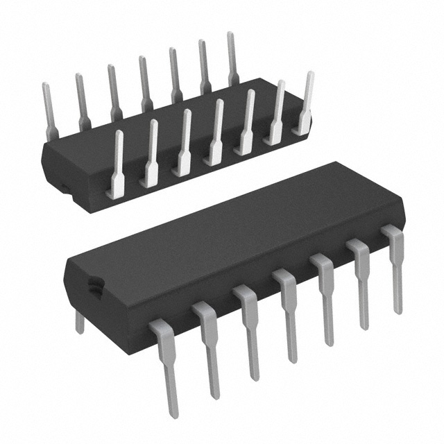
14-lead SOIC or PDIP package
0.5 or 1.0μs (typ.) internal dead time
RoHS compliant
Topology
Full-bridge
VOFFSET
600 V
Io+ & I o- (typical)
Deadtime (typical)
180 mA & 260 mA
1.0 μs (IRS2453D)
0.5 μs (IRS24531D)
Package Options
14 Lead PDIP
IRS2453DPbF
14 Lead SOIC
(Narrow Body)
IRS2453(1)DSPbF
Ordering Information
Standard Pack
Base Part Number
Package Type
PDIP14
IRS2453D(S)
Complete Part Number
Form
Quantity
Tube/Bulk
25
IRS2453DPBF
Tube/Bulk
55
IRS2453DSPBF
Tape and Reel
2500
IRS2453DSTRPBF
Tube/Bulk
55
IRS24531DSPBF
Tape and Reel
2500
IRS24531DSTRPBF
SOIC14N
IRS24531DS
1
www.irf.com
SOIC14N
© 2016 International Rectifier
April 27, 2016
�IRS2453(1)D(S)
Table of Contents
Page
Ordering Information
1
Description
3
Typical Connection Diagram
3
Qualification Information
4
Absolute Maximum Ratings
5
Recommended Operating Conditions
6
Recommended Component Values
6
Electrical Characteristics
7
Functional Block Diagram
9
Input / Output Pin Equivalent Circuit Diagram
10
Lead Definitions
11
Lead Assignments
11
Application Information and Additional Details
12
Package Details
15
Tape and Reel Details
16
Part Marking Information
17
2
www.irf.com
© 2016 International Rectifier
April 27, 2016
�IRS2453(1)D(S)
Description
The IRS2453(1)D is based on the popular IR2153 self-oscillating half-bridge gate driver IC, and incorporates a
high voltage full-bridge gate driver with a front end oscillator similar to the industry standard CMOS 555 timer.
HVIC and latch immune CMOS technologies enable ruggedized monolithic construction. The output driver
features a high pulse current buffer stage designed for minimum driver cross-conduction. Noise immunity is
achieved with low di/dt peak of the gate drivers, and with an under voltage lockout hysteresis greater than 1.5 V.
The IRS2453(1)D also includes latched and non-latched shutdown pins.
Typical Connection Diagram
+ AC rectified line
1 VCC
2 COM
3 CT
4 RT
5 SD
6 LO1
7 LO2
VB1 14
IRS2453(1)D
15 V
HO1 13
VS1 12
NC 11
VB2 10
HO2 9
VS2 8
LOAD
- AC rectified line
3
www.irf.com
© 2016 International Rectifier
April 27, 2016
�IRS2453(1)D(S)
Qualification Information
†
Qualification Level
Moisture Sensitivity Level
Machine Model
ESD
Human Body Model
IC Latch-Up Test
RoHS Compliant
†
††
†††
††
Industrial
Comments: This family of ICs has passed JEDEC’s
Industrial qualification. IR’s Consumer qualification level is
granted by extension of the higher Industrial level.
†††
MSL2 260°C
SOIC14
(per IPC/JEDEC J-STD-020)
Not applicable
PDIP14
(non-surface mount package style)
Class C
(per JEDEC standard JESD22-A115)
Class 2
(per EIA/JEDEC standard EIA/JESD22-A114)
Class I, Level A
(per JESD78)
Yes
Qualification standards can be found at International Rectifier’s web site http://www.irf.com/
Higher qualification ratings may be available should the user have such requirements. Please contact
your International Rectifier sales representative for further information.
Higher MSL ratings may be available for the specific package types listed here. Please contact your
International Rectifier sales representative for further information.
4
www.irf.com
© 2016 International Rectifier
April 27, 2016
�IRS2453(1)D(S)
Absolute Maximum Ratings
Absolute maximum ratings indicate sustained limits beyond which damage to the device may occur. All voltage
parameters are absolute voltages referenced to COM, all currents are defined positive into any lead. The thermal
resistance and power dissipation ratings are measured under board mounted and still air conditions.
Symbol
Definition
Min.
Max.
Units
VB1,
High side floating supply voltage
-0.3
625
VB2
VS1,
VB - 25
VB + 0.3
High side floating supply offset voltage
VS2
VHO1,
VS - 0.3
VB + 0.3
High side floating output voltage
VHO2
V
VLO1,
VCC + 0.3
Low side output voltage
-0.3
VLO2
VRT
RT pin voltage
VCC + 0.3
-0.3
VCT
CT pin voltage
-0.3
VCC + 0.3
VSD
SD pin voltage
-0.3
VCC + 0.3
IRT
RT pin current
-5
5
ICC
Supply current (†)
---
25
Allowable offset voltage slew rate
-50
50
PD
Maximum power dissipation @ TA≤ +25 ºC, PDIP14
---
1.6
PD
Maximum power dissipation @ TA ≤ +25 ºC, SOIC14N
---
1.0
RθJA
Thermal resistance, junction to ambient, PDIP14
---
75
RθJA
Thermal resistance, junction to ambient, SOIC14N
---
120
TJ
Junction temperature
-55
150
TS
Storage temperature
-55
150
TL
Lead temperature (soldering, 10 seconds)
---
300
dVS/dt
†
mA
V/ns
W
ºC/W
ºC
This IC contains a zener clamp structure between the chip VCC and COM which has a nominal
breakdown voltage of 15.6 V. Please note that this supply pin should not be driven by a DC, low
impedance power source greater than the VCLAMP specified in the Electrical Characteristics section.
5
www.irf.com
© 2016 International Rectifier
April 27, 2016
�IRS2453(1)D(S)
Recommended Operating Conditions
For proper operation the device should be used within the recommended conditions.
Symbol
Definition
Min.
VBS1,
VCC - 0.7
High side floating supply voltage
VBS2
VS1, VS2 Steady state high side floating supply offset voltage
-3.0 (†)
Max.
Units
VCLAMP
V
600
VCC
Supply voltage
VCCUV+
VCLAMP
ICC
Supply current
(††)
5
mA
TJ
Junction temperature
-25
125
ºC
† It is recommended to avoid output switching conditions where negative-going spikes at the VS node
would decrease VS below ground by more than -5V.
†† Enough current should be supplied to the VCC pin of the IC to keep the internal 15.6 V zener diode
clamping the voltage at this pin.
Recommended Component Values
Symbol
Component
RT
Timing resistor value
CT
CT pin capacitor value
Min.
Max.
Units
1
---
k
330
---
pF
VBIAS (VCC, VBS) = 14 V, VS=0 V and TA = 25 °C, CLO1=CLO2 = CHO1=CHO2 = 1nF.
IRS2453(1)D
IRS2453DFrequency
Frequencyvs.
vs.RT
RT
1000000
CT Values
Frequency (Hz)
100000
330pf
470pF
10000
1nF
2.2nF
1000
4.7nF
10nF
100
10
1000
10000
100000
1000000
RT (Ohm)
6
www.irf.com
© 2016 International Rectifier
April 27, 2016
�IRS2453(1)D(S)
Electrical Characteristics
VBIAS (VCC, VBS) = 14 V, CT = 1nF and TA = 25 °C unless otherwise specified. The VO and IO parameters are
referenced to COM and are applicable to the respective output leads:
HO or LO. CLO1=CLO2=CHO1=CHO2=1nF.
Symbol
Definition
Min
Typ
Max
Units Test Conditions
Low Voltage Supply Characteristics
VCCUV+
Rising VCC under voltage lockout threshold
10.0
11.0
12.0
VCCUVVCCUVH
YS
IQCCUV
Falling VCC under voltage lockout threshold
8.0
9.0
10.0
VCC under voltage lockout hysteresis
Micropower startup VCC supply current
1.5
2.0
2.4
---
140
200
IQCC
Quiescent VCC supply current
---
1.3
2.0
ICC_20K
VCC supply current at fosc (RT = 36.5 kΩ)
---
3.5
ICCFLT
VCC supply current when SD > VSD
---
3.0
360
360
500
µA
14.6
15.6
16.6
V
---
3
10
VCLAMP
VCC Zener clamp voltage
V
µA
VCC VCCUV-
mA
ICC = 5 mA
Floating Supply Characteristics
IQBS1UV,
IQBS2UV
Micropower startup VBS supply current
µA
IQBS1,
IQBS2
Quiescent VBS supply current
---
30
100
VBS1UV+,
VBS2UV+
VBS supply under voltage positive going
threshold
8.0
9.0
10.0
VBS1UV-,
VBS2UV-
VBS supply under voltage negative going
threshold
7.0
8.0
9.0
ILK1, ILK2
Offset supply leakage current
---
---
50
19.6
20.2
20.8
88
94
100
RT pin duty cycle
48
50
52
%
CT pin current
---
0.05
1.0
A
ICTUV
VCT+
UV-mode CT pin pull down current
1
5
---
mA
Upper CT ramp voltage threshold
---
9.3
---
VCT-
Lower CT ramp voltage threshold
---
4.7
---
---
10
50
---
100
300
---
10
50
---
100
300
---
0
100
V
A
Oscillator I/O Characteristics
fOSC
d
ICT
VRT+
VRT-
VRTUV
7
Oscillator frequency
kHz
Low level RT output voltage
www.irf.com
© 2016 International Rectifier
VB = VS = 600
V
RT = 36.5 k
RT = 7.15 k
fo < 100 kHz
VCC = 7 V
V
High level RT output voltage, VCC - VRT
UV-mode RT output voltage
VCC VCCUV, VCC = VBS
mV
IRT = 100 A
RT = 140 k
IRT = 1 mA
RT = 14 k
IRT = 100 A
RT = 140 k
IRT = 1 mA
RT = 14 k
VCC VCCUV-
April 27, 2016
�IRS2453(1)D(S)
Electrical Characteristics
VBIAS (VCC, VBS) = 14 V, CT = 1nF and TA = 25 °C, unless otherwise specified. The VO and IO parameters are
referenced to COM and are applicable to the respective output leads:
HO or LO. CLO1=CLO2=CHO1=CHO2=1nF.
Symbol
Definition
Min
Typ
Max
Units Test Conditions
Gate Driver Output Characteristics
VOH
High level output voltage, VBIAS - VO
---
VCC
---
VOL
Low level output voltage, VO
---
COM
---
IO = 0 A
V
VOL_UV
UV-mode output voltage, VO
---
COM
---
tr
Output rise time
---
120
200
tf
Output fall time
---
50
100
tsd
Shutdown propagation delay
---
250
---
IRS2453D
0.8
1.0
1.40
td
Output dead time (HO or LO)
IRS24531D
0.4
0.5
0.7
IO+
Output source current
---
180
---
IO-
Output sink current
---
260
---
Shutdown threshold at SD pin (latched)
1.8
2.0
2.3
CT voltage shutdown threshold (non-latched)
2.2
2.3
2.5
IO = 0 A,
VCC
VCCUV-
ns
s
mA
Shutdown
VSD
V
VCTSD
--VRTSD
10
50
SD mode RT output voltage, VCC - VRT
mV
---
100
300
VB when the bootstrap FET is on
13.7
14.0
---
VB source current when FET is on
40
55
---
VB source current when FET is on
10
12
---
IRT = 100 A,
RT = 140 k
VCT = 0 V
IRT = 1 mA,
RT = 14 k
VCT = 0 V
Bootstrap FET Characteristics
VB1_ON
VB2_ON
IB1_CAP
IB2_CAP
IB1_10 V
IB2_10 V
8
V
CBS=0.1 μF
mA
www.irf.com
© 2016 International Rectifier
VB=10 V
April 27, 2016
�IRS2453(1)D(S)
Functional Block Diagram
RT 4
14 VB1
R
Q
HV
Level
Shift
+
-
S
R
R
+
-
Q
DEAD
TIME
12 VS1
PULSE
GEN
S
13 HO1
R
PULSE
FILTER
BOOTSTRAP
DRIVE
Q
R/2
+
-
CT 3
S Q
R1
R2 Q
DEAD
TIME
DELAY
6
LO1
R/2
SD 5
S
2.0V
10 VB2
Q
R
HV
Level
Shift
Q
PULSE
FILTER
R
9 HO2
S
8 VS2
PULSE
GEN
BOOTSTRAP
DRIVE
UV
DETECT
1 VCC
15.4V
DELAY
7 LO2
2
9
www.irf.com
© 2016 International Rectifier
COM
April 27, 2016
�IRS2453(1)D(S)
Input / Output Pin Equivalent Circuit Diagrams:
VB1
VB2
ESD
Diode
ESD
Diode
25V
HO1
25V
HO2
ESD
Diode
ESD
Diode
VS1
VS2
600V
600V
VCC
VCC
ESD
Diode
ESD
Diode
LO1
LO2
25V
25V
ESD
Diode
ESD
Diode
COM
COM
VCC
VCC
ESD
Diode
ESD
Diode
25V
SD
RESD
ESD
Diode
ESD
Diode
COM
VCC
ESD
Diode
CT
RESD
ESD
Diode
COM
10
www.irf.com
© 2016 International Rectifier
April 27, 2016
�IRS2453(1)D(S)
Lead Definitions
Pin
Symbol
1
VCC
Description
Logic and internal gate drive supply voltage
2
COM
IC power and signal ground
3
CT
Oscillator timing capacitor input
4
RT
Oscillator timing resistor input
5
SD
Shutdown input
6
LO1
Low side gate driver output
7
LO2
Low side gate driver output
8
VS2
High voltage floating supply return
9
HO2
High side gate driver output
10
VB2
High side gate driver floating supply
11
NC
No connect
12
VS1
High voltage floating supply return
13
HO1
High side gate driver output
14
VB1
High side gate driver floating supply
Lead Assignment
11
www.irf.com
1
COM
2
CT
3
RT
4
SD
5
LO1
6
LO2
7
© 2016 International Rectifier
14
IRS2453(1)D(S)
VCC
VB1
13 HO1
12
VS1
11
NC
10
VB2
9
HO2
8
VS2
April 27, 2016
�IRS2453(1)D(S)
Application Information and Additional Details
Timing Diagram
VCCUV+
VCC
Fault mode
VCT