July 09, 2008
IRS2530D(S)
DIM8
DIMMING BALLAST CONTROL IC
Product Summary
IC Features
•
•
•
•
•
•
•
•
•
•
•
TM
Dimming ballast control plus half-bridge driver
Closed-loop lamp current dimming control
Internal non-ZVS protection
Internal crest factor protection
Programmable preheat time
Fixed dead-time (2.0μs typ.)
Lamp insert auto-restart
Internal bootstrap MOSFET
Internal 15.6V zener clamp diode on Vcc
Micropower startup (250μA)
Latch immunity and ESD protection
Topology
Half-Bridge
VOFFSET
600 V
VOUT
VCC
IO+ & IO- (typical)
180mA & 260mA
Deadtime (typical)
2.0μs
Package Types
Ballast System Features
•
•
•
•
•
•
•
•
•
Single chip dimming solution
Simple lamp current dimming control method
Single lamp current sensing resistor required
No half-bridge current-sensing resistor required
No external protection circuits required (fully
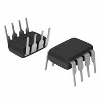
PDIP8
SO8
internal)
Flash-free lamp start at all dimming levels
Large reduction in component count
Typical applications
Easy to use for fast design cycle time
•
Linear dimming ballast (down to 10%)
Increased manufacturability and reliability
•
3-way dimming ballast
•
Multi-level switch dimming ballast
Typical Connection Diagram
L
AC
LINE
INPUT
F1
LF
BR1
RVCC1
N
RVCC2
RLIM1
CF
CBUS
VCC
CVCC2
COM
VB
1
8
IRS2530D
CVCC1
RLIM2
2
CDIM
DIM
CVCO
VCO
3
4
7
6
5
RHO
MHS
HO
VS
LO
LRES:A
CDC
CBS
LRES:B
CSNUB
RLO
CRES
MLS
SPIRAL
CFL LAMP
CH1
DCP2
RDIM1
1-10V
DIM
INPUT
RLMP2
CPH RVCO
(+)
RLMP1
CH2
CFB
RFB
DCP1
LRES:C
RDIM2
(-)
RCS
www.irf.com
© 2008 International Rectifier
1
�IRS2530D(S)
Table of Contents
Page
Description
3
Qualification Information
4
Absolute Maximum Ratings
5
Recommended Operating Conditions
6
Electrical Characteristics
7
Input/Output Pin Equivalent Circuit Diagram
9
Lead Definitions
10
Lead Assignments
10
State Diagram
11
Application Information and Additional Details
12
Package Details
20
Tape and Reel Details
21
Part Marking Information
22
Ordering Information
23
www.irf.com
© 2008 International Rectifier
2
�IRS2530D(S)
Description
This IC takes full advantage of IR’s patented ballast and high-voltage technologies to realize a simple, highperformance dimming ballast solution. A single high-voltage pin senses the half-bridge current and voltage
to perform necessary ballast protection functions. The DC dim input voltage reference and the AC lamp
current feedback have been coupled together allowing a single pin to be used for dimming. Combining these
high-voltage control algorithms together with a simple dimming method in a single 8-pin IC results in a large
reduction in component count, an increase in manufacturability and reliability, a reduced design cycle time,
while maintaining high dimming ballast system performance
Block Diagram
Bootstrap
MOSFET
VCC 1
Driver
Logic
UVLO
COM 2
High-Side
Half-bridge
Driver
8
VB
7
HO
6
VS
5
LO
1uA
Voltage
Controlled
Oscillator
VCO 4
Fault
Logic
Crest
Factor
Protection
Non-ZVS
Protection
Dimming
Control
DIM
Half-bridge
Voltage
Sensing
Low-Side
Half-bridge
Driver
3
Restart
Logic
www.irf.com
© 2008 International Rectifier
3
�IRS2530D(S)
†
Qualification Information
Qualification Level
Moisture Sensitivity Level
Machine Model
ESD
Human Body Model
IC Latch-Up Test
RoHS Compliant
Industrial††
Comments: This family of ICs has passed JEDEC’s Industrial
qualification. IR’s Consumer qualification level is granted by
extension of the higher Industrial level.
MSL2†††
SOIC8
(per IPC/JEDEC J-STD-020C)
Not applicable
PDIP8
(non-surface mount package style)
Class C
(per JEDEC standard EIA/JESD22-A115)
Class 3A
(per EIA/JEDEC standard JESD22-A114)
Class I, Level A
(per JESD78A)
Yes
†
††
Qualification standards can be found at International Rectifier’s web site http://www.irf.com/
Higher qualification ratings may be available should the user have such requirements. Please contact
your International Rectifier sales representative for further information.
†††
Higher MSL ratings may be available for the specific package types listed here. Please contact your
International Rectifier sales representative for further information.
www.irf.com
© 2008 International Rectifier
4
�IRS2530D(S)
Absolute Maximum Ratings
Absolute Maximum Ratings indicate sustained limits beyond which damage to the device may occur. All
voltage parameters are absolute voltages referenced to COM, all currents are defined positive into any lead.
The Thermal Resistance and Power Dissipation ratings are measured under board mounted and still air
conditions.
Symbol
Definition
Min.
Max.
VB
High-Side Floating Supply Voltage
-0.3
625
VS
High-Side Floating Supply Offset Voltage
VB - 25
VB + 0.3
VHO
High-Side Floating Output Voltage
VS - 0.3
VB + 0.3
VLO
Low-Side Output Voltage
-0.3
VCC + 0.3
VVCO
VCO Input Voltage
-0.3
6
VDIM
DIM Input Voltage
-0.3
VCC + 0.3
††
†
ICC
---
20
-500
500
dVS/dt
Supply Current
Maximum allowable current at LO, HO and PFC due to
external power transistor Miller effect.
Allowable VS Pin Voltage Slew Rate
-50
50
PD
Maximum Power Dissipation @ TA ≤ +25ºC, 8-Pin DIP
---
1.0
PD
Maximum Power Dissipation @ TA ≤ +25ºC, 8-Pin SOIC
---
0.625
RθJA
Thermal Resistance, Junction to Ambient, 8-Pin DIP
---
85
RθJA
Thermal Resistance, Junction to Ambient, 8-Pin SOIC
---
128
TJ
Junction Temperature
-55
150
TS
Storage Temperature
-55
150
TL
Lead Temperature (Soldering, 10 seconds)
---
300
IOMAX
Units
V
mA
V/ns
W
ºC/W
ºC
†
This IC contains a zener clamp structure between the chip VCC and COM which has a nominal
breakdown voltage of 15.6V. This supply pin should not be driven by a DC, low impedance power
source greater than the VCLAMP specified in the Electrical Characteristics section.
††
This IC contains a zener clamp structure between the chip VCO and COM which has a nominal
breakdown voltage of 7.25V. This pin should not be driven by a DC, low impedance power source
greater than the VVCOMAX specified in the Electrical Characteristics section.
www.irf.com
© 2008 International Rectifier
5
�IRS2530D(S)
Recommended Operating Conditions
For proper operation the device should be used within the recommended conditions.
Symbol
VBS
Definition
Min.
Max.
Units
VCC - 0.7
VCLAMP
V
600
V
VCCUV+ + 0.1V
VCLAMP
V
VCC
High-Side Floating Supply Voltage
Steady State High-Side Floating Supply
Offset Voltage
Supply Voltage
ICC
Supply Current
---
5
mA
VVCO
VCO Pin Voltage
0
6
V
TJ
Junction Temperature
-40
125
ºC
VS
†††
-3.0
†††
Care should be taken to avoid output switching conditions where the VS node decreases below
COM by more than 5V.
www.irf.com
© 2008 International Rectifier
6
�IRS2530D(S)
Electrical Characteristics
VCC=VBS=14V, VS=0V, CVCC=CBS=0.1μF, CVCO=CDIM=10nF, CLO=CHO=1nF, and TA = 25°C unless
otherwise specified. The output voltage and current (VO and IO) parameters are referenced to COM and are
applicable to the respective HO and LO output leads.
Symbol
Definition
Min
Typ
Max
Units
Test Conditions
Low Voltage Supply Characteristics
VCLAMP
VCC Zener Clamp Voltage
14.6
15.6
16.6
VCCUV+
Rising VCC UVLO+ Threshold
11.5
12.5
13.5
VCCUV-
Falling VCC UVLO- Threshold
9.5
10.5
11.5
VCC Undervoltage Lockout Hysteresis
1.5
2.0
3.0
IQCCUV
Micropower Startup VCC Supply Current
---
250
---
µA
VCC = 8V
ICCDIM
DIM Mode VCC Supply Current
---
4.5
---
mA
MODE = DIM
IQCCFLT
Fault Mode VCC Supply Current
VCO Pin Zener Clamp Voltage
---
375
---
µA
MODE = FAULT
---
7.25
---
V
MODE = DIM
VBS Supply Current
---
2
3
mA
MODE = DIM
IQBSUV
UVLO Mode VBS Quiescent Current
---
---
50
µA
VBS = 7V
VBSUV+
Rising VBS Supply Undervoltage
Threshold
Falling VBS Supply Undervoltage
Threshold
Offset Supply Leakage Current
8.0
9.0
10.0
7.0
8.0
9.0
---
---
50
VCCUVHY
VVCOMAX
ICC = 10mA
V
Floating Supply Characteristics
IBS
VBSUVILK
V
μA
VB = VS = 600V
Ballast Control Characteristics
fMIN
Minimum Output Frequency
32.0
34.2
36.4
fMAX
Maximum Output Frequency
---
115
---
Duty Cycle
---
50
---
%
Output Deadtime (HO or LO)
---
2.0
---
µs
MODE = ALL
VCO Pin Charging Current
---
1
---
µA
MODE = PH/IGN
VLOSD+
LO Pin Shutdown Threshold
---
8.75
---
VLOSD-
LO Pin Re-start Threshold
---
8.5
---
VZVSTH
VS Non-ZVS Detection Threshold
---
4.5
---
VCO Fault Rising Threshold
---
4.0
---
Crest factor peak-to-average fault factor
---
5.5
---
d
DT
IVCO
VVCOFLT+
CSCF
www.irf.com
kHz
VCO = 6V
VCO = 0V
MODE = FAULT
V
MODE = FAULT
MODE = DIM, LO
= HIGH
V
MODE = PH/IGN
N/A
MODE = DIM
VS offset = 0.5V
© 2008 International Rectifier
7
�IRS2530D(S)
Electrical Characteristics
VCC=VBS=14V, VS=0V, CVCC=CBS=0.1µF, CVCO=CDIM=10nF, CLO=CHO=1nF, and TA = 25°C unless
otherwise specified. The output voltage and current (VO and IO) parameters are referenced to COM and are
applicable to the respective HO and LO output leads.
Symbol
Definition
Min
Typ
Max
Units
---
0.0
---
V
Test Conditions
Dimming Control Characteristics
VDIMREG
DIM Regulation Threshold
MODE = DIM
Gate Driver Output Characteristics (HO and LO)
VOH
High-Level Output Voltage
---
VCC
---
IO = 0A
VOL
Low-Level Output Voltage
---
COM
---
IO = 0A
---
IO = 0A,
VCC ≤ VCCUV-
VOL_UV
---
UV-Mode Output Voltage
COM
tr
Output Rise Time
---
120
220
tf
Output Fall Time
---
50
80
tSD
Shutdown Propagation Delay
---
350
---
IO+
Output source current
---
180
---
IO-
Output sink current
---
260
---
ns
mA
Bootstrap FET Characteristics
VB_ON
VB when the bootstrap FET is on
---
13.3
---
IB_CAP
VB source current when FET is on
30
55
---
IB_10V
VB source current when FET is on
8
12
---
www.irf.com
V
mA
CBS = 0.1µF
VB = 10V
© 2008 International Rectifier
8
�IRS2530D(S)
I/O Pin Equivalent Circuit Diagrams
www.irf.com
© 2008 International Rectifier
9
�IRS2530D(S)
Lead Definitions
Pin #
Symbol
Description
1
VCC
Logic and internal gate drive supply voltage
2
COM
IC power and signal ground
3
DIM
Dimming DC reference and AC lamp current feedback input
4
VCO
Voltage-controlled oscillator (VCO) input
5
LO
Half-bridge low-side gate driver output
6
VS
High voltage floating supply return and half-bridge sensing input
7
HO
High-side gate driver output
8
VB
High-side gate driver floating supply
Lead Assignments
1
COM
2
DIM
3
VCO
4
8
IRS2530D
VCC
www.irf.com
VB
7 HO
6 VS
5 LO
© 2008 International Rectifier
10
�IRS2530D(S)
State Diagram
Power Off
VCC > 0V
UVLO Mode
Half-Bridge Off
VCC < 10.5V (VCCUV-)
or
LO > 8.75V (VLOSD+)
(Lamp Removed)
IQCCUV ≅ 250μA
VCO = 0V
HO Off
LO Open Circuit
VCC > 12.5V (VCCUV+)
and
LO < 8.5V (VLOSD-)
(Lamp Inserted)
VCC < 10.5V (VCCUV-)
FAULT Mode
Fault Latch Set
Half-Bridge Off
IQCCUV ≅ 250μA
HO Off
LO Open Circuit
VCO > 4.0V
(VVCOFLT+)
(Lamp non-strike)
PH/IGN Mode
Half-Bridge Oscillating
Freq ramps from fMAX to fMIN
VCO Charging (1μA)
non-ZVS Disabled
Crest Factor Disabled
Lamp Ignites
CF > 5.5 (lamp removal)
DIM Mode
non-ZVS
ZVS
freq = freq + df
ZVS OK
Half-Bridge Oscillating @fDIM
Dimming Loop Enabled
non-ZVS Enabled
Crest Factor Enabled
www.irf.com
© 2008 International Rectifier
11
�IRS2530D(S)
Application Information and Additional Details
Information regarding the following topics is included as subsections within this section of the datasheet:
•
•
•
•
•
•
•
•
UVLO Mode and IC Supply Circuitry
Preheat/Ignition (PH/IGN) Mode
Dim Mode
Non Zero-Voltage Switching (ZVS) Protection
Crest Factor Over-current Protection
Fault Mode and Lamp Reset
Component Selection
PCB Layout Guidelines
UVLO Mode and IC Supply Circuitry
The Under-Voltage Lock-Out Mode (UVLO) is defined as the state the IC is in when VCC is below the turn-on
threshold of the IC, VCCUV+ (12.5 V, typical), and LO is above the shutdown threshold, VLOSD+ (8.75 V, typical).
The UVLO circuit is designed to maintain an ultra-low supply current IQCCUV (
很抱歉,暂时无法提供与“IRS2530DPBF”相匹配的价格&库存,您可以联系我们找货
免费人工找货