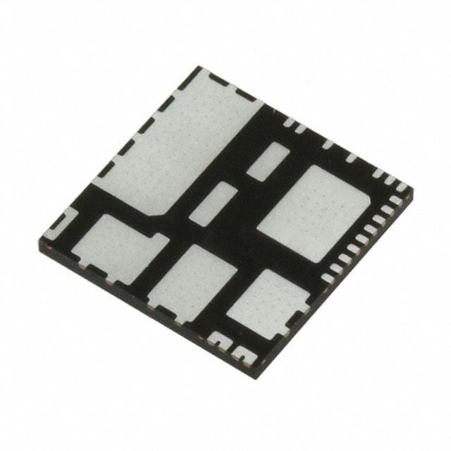
IRSM836-035MA
3A, 500V
Integrated Power Module for
Small Appliance Motor Drive Applications
Description
IRSM836-035MA is a 3A, 500V Integrated Power Module (IPM) designed for advanced appliance motor drive
applications such as energy efficient fans and pumps. IR's technology offers an extremely compact, high
performance AC motor-driver in an isolated package. This advanced IPM offers a combination of IR's low RDS(on)
Trench MOSFET technology and the industry benchmark 3-phase high voltage, rugged driver in a small PQFN
package. At only 12x12mm and featuring integrated bootstrap functionality, the compact footprint of this surfacemount package makes it suitable for applications that are space-constrained. Integrated over-current protection,
fault reporting and under-voltage lockout functions deliver a high level of protection and fail-safe operation.
IRSM836-035MA functions without a heat sink.
Features
Integrated gate drivers and bootstrap functionality
Open-source for leg-shunt current sensing
Protection shutdown pin
Low RDS(on) Trench FREDFET
Under-voltage lockout for all channels
Matched propagation delay for all channels
Optimized dV/dt for loss and EMI trade offs
3.3V Schmitt-triggered active high input logic
Cross-conduction prevention logic
Motor power range up to ~110W, without heat sink
Isolation 1500VRMS min
Base Part Number
Package Type
IRSM836-035MA
36L
PQFN 12 x 12 mm
IRSM836-035MA
Standard Pack
Orderable Part Number
Form
Quantity
Tape and Reel
2000
IRSM836-035MATR
Tray
800
IRSM836-035MA
All part numbers are PbF
1
www.irf.com
© 2015 International Rectifier
March 24, 2015
�IRSM836-035MA
Internal Electrical Schematic
VB1 VB2 VB3
IRSM836-035MA
V+
VCC
HIN1
HIN2
HIN3
LIN1
LIN2
LIN3
FAULT
ITRIP
EN
RCIN
U, VS1
V, VS2
W, VS3
600V
3-Phase
Driver
HVIC
COM
VSS
VRU
VRV
VRW
Absolute Maximum Ratings
Absolute maximum ratings indicate sustained limits beyond which damage to the module may occur. These are not tested at
manufacturing. All voltage parameters are absolute voltages referenced to VSS unless otherwise stated in the table.
Symbol
Description
Min
Max
Unit
BVDSS
MOSFET Blocking Voltage
---
500
V
IO @ T=25°C
DC Output Current per MOSFET
---
3
IOP
Pulsed Output Current (Note 1)
---
20
Pd @ TC=25°C
Maximum Power Dissipation per MOSFET
---
36
W
VISO
Isolation Voltage (1min) (Note 2)
---
1500
VRMS
TJ
Operating Junction Temperature
-40
150
°C
TL
Lead Temperature (Soldering, 30 seconds)
---
260
°C
TS
Storage Temperature
-40
150
°C
VS1,2,3
High Side Floating Supply Offset Voltage
VB1,2,3 - 20
VB1,2,3 +0.3
V
VB1,2,3
High Side Floating Supply Voltage
-0.3
500
V
VCC
Low Side and Logic Supply voltage
-0.3
20
V
VSS -0.3
VCC+0.3
V
VIN
Input Voltage of LIN, HIN, ITRIP, EN, RCIN, FLT
Note 1: Pulse Width = 100µs, TC =25°C, Duty=1%.
Note 2: Characterized, not tested at manufacturing
2
www.irf.com
© 2015 International Rectifier
A
March 24, 2015
�IRSM836-035MA
Recommended Operating Conditions
Symbol
Description
V+
Positive DC Bus Input Voltage
Min
Max
Unit
---
400
V
VS1,2,3
High Side Floating Supply Offset Voltage
(Note 3)
400
V
VB1,2,3
High Side Floating Supply Voltage
VS+10
VS+20
V
VCC
Low Side and Logic Supply Voltage
11.5
18.5
V
VIN
Input Voltage of LIN, HIN, ITRIP, EN, FLT
0
5
V
Fp
PWM Carrier Frequency
---
20
kHz
The Input/Output logic diagram is shown in Figure 1. For proper operation the module should be used within the
recommended conditions. All voltages are absolute referenced to COM. The V S offset is tested with all supplies biased at 15V
differential.
Note 3: Logic operational for Vs from COM-5V to COM+250V. Logic state held for Vs from COM-5V to COM-VBS.
Static Electrical Characteristics
o
(VCC-COM) = (VB-VS) = 15 V. TA = 25 C unless otherwise specified. The VIN and IIN parameters are referenced to VSS and are
applicable to all six channels. The VCCUV parameters are referenced to VSS. The VBSUV parameters are referenced to VS.
Symbol
Description
Min
Typ
Max
Units
BVDSS
Drain-to-Source Breakdown Voltage
500
---
---
V
TJ=25°C, ILK=250µA
ILKH
Leakage Current of High Side FET’s in
Parallel
10
µA
TJ=25°C, VDS=500V
ILKL
Leakage Current of Low Side FET’s in
Parallel Plus Gate Drive IC
15
µA
TJ=25°C, VDS=500V
RDS(ON)
Drain to Source ON Resistance
---
1.85
2.2
Ω
TJ=25°C, VCC=15V, Id = 1A
VIN,th+
Positive Going Input Threshold
2.5
---
---
V
VIN,th-
Negative Going Input Threshold
---
---
0.8
V
VCCUV+,
VBSUV+
VCC and VBS Supply Under-Voltage,
Positive Going Threshold
8
8.9
9.8
V
VCCUV-,
VBSUV-
VCC and VBS supply Under-Voltage,
Negative Going Threshold
7.4
8.2
9
V
VCCUVH,
VBSUVH
VCC and VBS Supply Under-Voltage
Lock-Out Hysteresis
---
0.7
---
V
IQBS
Quiescent VBS Supply Current VIN=0V
---
---
125
µA
IQCC
Quiescent VCC Supply Current VIN=0V
---
---
3.35
mA
IQCC, ON
Quiescent VCC Supply Current VIN=4V
---
---
10
mA
IIN+
Input Bias Current VIN=4V
---
100
160
µA
IIN-
Input Bias Current VIN=0V
---
--
1
µA
ITRIP+
ITRIP Bias Current VITRIP=4V
---
5
40
µA
ITRIP-
ITRIP Bias Current VITRIP=0V
---
--
1
µA
VIT, TH+
ITRIP Threshold Voltage
0.37
0.46
0.55
V
VIT, TH-
ITRIP Threshold Voltage
---
0.4
---
V
3
www.irf.com
Conditions
© 2015 International Rectifier
March 24, 2015
�IRSM836-035MA
VIT, HYS
ITRIP Input Hysteresis
---
0.06
---
V
RBR
Internal Bootstrap Equivalent Resistor
Value
---
200
---
Ω
VRCIN,TH
RCIN Positive Going Threshold
---
8
---
V
RON,FLT
FLT Open-Drain Resistance
---
50
100
Ω
Min
Typ
Max
Units
0.7
1.5
µs
TJ=25°C
Dynamic Electrical Characteristics
o
(VCC-COM) = (VB-VS) = 15 V. TA = 25 C unless otherwise specified.
Symbol
Description
Conditions
TON
Input to Output Propagation Turn-On
Delay Time
---
TOFF
Input to Output Propagation Turn-Off
Delay Time
---
0.7
1.5
µs
TFIL,IN
Input Filter Time (HIN, LIN)
200
330
---
ns
VIN=0 & VIN=4V
TFIL,EN
Input Filter Time (EN)
100
200
---
ns
VIN=0 & VIN=4V
TBLT-ITRIP
ITRIP Blanking Time
100
330
ns
VIN=0 & VIN=4V, VI/Trip=5V
TFLT
Itrip to Fault
---
600
1000
ns
VIN=0 & VIN=4V
TEN
EN Falling to Switch Turn-Off
700
1000
ns
VIN=0 & VIN=4V
TITRIP
ITRIP to Switch Turn-Off Propagation Delay
950
1300
ns
ID=1A, V =50V, See Figure 3
Max
Units
+
ID=1mA, V =50V
See Fig.2
---
+
MOSFET Avalanche Characteristics
Symbol
Description
Min
Typ
Conditions
EAS
Single Pulse Avalanche Energy
--150
--mJ
Note 4
Note 4: From characterization of TO-220 packaged devices. Starting TJ=25°C, L=93mH, VDD=150V, IAS=1.8A
Thermal and Mechanical Characteristics
Symbol
Description
Rth(J-CT)
Rth(J-CB)
4
Min
Typ
Max
Units
Conditions
Total Thermal Resistance Junction to
Case Top
---
27.4
---
°C/W
One device
Total Thermal Resistance Junction to
Case Bottom
---
2.2
---
°C/W
One device
www.irf.com
© 2015 International Rectifier
March 24, 2015
�IRSM836-035MA
Qualification Information†
††
Qualification Level
Industrial
(per JEDEC JESD 47E)
Moisture Sensitivity Level
MSL3
(per IPC/JEDEC J-STD-020C)
†††
Machine Model
Class B
(per JEDEC standard JESD22-A115)
Human Body Model
Class 2
(per standard ESDA/JEDEC JS-001-2012)
ESD
RoHS Compliant
Yes
†
Qualification standards can be found at International Rectifier’s web site http://www.irf.com/
††
Higher qualification ratings may be available should the user have such requirements. Please contact
your International Rectifier sales representative for further information.
†††
Higher MSL ratings may be available for the specific package types listed here. Please contact your
International Rectifier sales representative for further information.
5
www.irf.com
© 2015 International Rectifier
March 24, 2015
�IRSM836-035MA
Input/Output Pin Equivalent Circuit Diagrams
VB
ESD
Diode
20 V
Clamp
HO
ESD
Diode
V CC
HIN,
LIN,
or EN
VS
ESD
Diode
600 V
VCC
20 V
Clamp
ESD
Diode
33k
ESD
Diode
25 V
Clamp
VSS
LO
ESD
Diode
COM
VCC
VCC
ESD
Diode
ESD
Diode
RCIN or
FAULT
ITRIP
ESD
Diode
VSS
6
www.irf.com
ESD
Diode
1M
VSS
© 2015 International Rectifier
March 24, 2015
�IRSM836-035MA
Input-Output Logic Level Table
V+
Ho
Hin1,2,3
Gate
Driver
IC
U, V, W
Lo
Lin1,2,3
EN
Itrip
Hin1,2,3
Lin1,2,3
U,V,W
1
0
1
0
V+
1
0
0
1
0
1
0
0
0
off
1
1
X
X
off
0
X
X
X
off
HIN1,2,3
LIN1,2,3
ITRIP
U,V,W
Figure 1: Input/Output Logic Diagram
7
www.irf.com
© 2015 International Rectifier
March 24, 2015
�IRSM836-035MA
VDS
ID
ID
VDS
90% ID
50%
HIN /LIN
90% ID
50%
VDS
HIN /LIN
50%
HIN /LIN
HIN /LIN
50%
VCE
10% ID
10% ID
tf
tr
TON
TOFF
Figure 2a: Input to Output propagation turn-on
delay time.
Figure 2b: Input to Output propagation turn-off
delay time.
IF
VDS
HIN /LIN
Irr
trr
Figure 2c: Diode Reverse Recovery.
Figure 2: Switching Parameter Definitions
8
www.irf.com
© 2015 International Rectifier
March 24, 2015
�IRSM836-035MA
HIN1,2,3
LIN1,2,3
50%
50%
ITRIP
U,V,W
50%
50%
TITRIP
TFLT-CLR
Figure 3: ITRIP Timing Waveform
9
www.irf.com
© 2015 International Rectifier
March 24, 2015
�IRSM836-035MA
Module Pin-Out Description
Pin
1
Name
HIN3
Description
Logic Input for High Side Gate Driver - Phase 3
2
LIN1
Logic Input for Low Side Gate Driver - Phase 1
3
LIN2
Logic Input for Low Side Gate Driver - Phase 2
4
LIN3
Logic Input for Low Side Gate Driver - Phase 3
5
/FLT
Fault Output Pin
6
Itrip
Over-Current Protection Pin
7
EN
Enable Pin
8
RCin
Reset Programming Pin
9, 39
10, 11, 30,
37
12, 13
VSS, COM
Ground for Gate Drive IC and Low Side Gate Drive Return
U, VS1
Output 1, High Side Floating Supply Offset Voltage
VR1
Phase 1 Low Side FET Source
14, 15
VR2
Phase 2 Low Side FET Source
16, 17, 38
V, VS2
Output 2, High Side Floating Supply Offset Voltage
18, 19
W, VS3
Output 3, High Side Floating Supply Offset Voltage
20, 21
VR3
Phase 3 Low Side FET Source
22-29
V+
DC Bus Voltage Positive
31
VB1
High Side Floating Supply Voltage 1
32
VB2
High Side Floating Supply Voltage 2
33
VB3
High Side Floating Supply Voltage 3
34
VCC
15V Supply
35
HIN1
Logic Input for High Side Gate Driver - Phase 1
36
HIN2
Logic Input for High Side Gate Driver - Phase 2b
26
25
24
23
22
21
20
27
28
Top View
19
29
18
30
31
38
37
17
16
32
33
39
10
www.irf.com
All pins with the same name are
internally connected. For example,
pins 10, 11, 30 and 37 are
internally connected.
15
14
13
12
34
35
36
1 2 3 4 5 6 7 8 9
Note
Pads 37 and 38 can be omitted
from the PCB footprint and hence
do not need to be soldered
10
11
© 2015 International Rectifier
March 24, 2015
�IRSM836-035MA
Fault Reporting and Programmable Fault Clear Timer
The IRSM836-035MA provides an integrated fault reporting output and an adjustable fault clear timer.
There are two situations that would cause the IRSM836-035MA to report a fault via the FLT pin. The first is an
under-voltage condition of VCC and the second is when the ITRIP pin recognizes a fault.
The fault clear timer provides a means of automatically re-enabling the module operation a preset amount
of time after the fault condition has disappeared. When a fault condition occurs, the fault diagnostic output (FLT)
stays in the low state until the fault condition has been removed and the fault clear timer expires; once the fault
clear timer expires, the voltage on the FLT pin will return to the logic-high voltage. Figure 4a is a block-level
diagram that focuses on the fault diagnostic and fault clear timer functionality of the driver chip within the module.
The fault clear timer is defined with a simple resistor-capacitor (RC) network on the RCin pin, as shown in Figure
4b.
Figure 5 is a timing diagram showing the states of the FLT and RCin pins during both normal operation and
under a fault condition. Under normal operation, both FLT and RCin are in high impedance (open drain) states.
CRCIN is fully-charged, and FLT is pulled up high. When a fault condition occurs, RCin and FLT are pulled low to
VSS – CRCIN is discharged; once the fault condition has been removed, RCin returns to a high impedance state
and the fault clear timer begins – that is, CRCIN starts charging via RRCIN. tFLTCLR seconds later – when the RCin
voltage crosses a datasheet-defined threshold of VRCIN,TH, FLT returns to a high impedance state and the module
is operational again. tFLTCLR is determined by a simple RC network, shown in Figure 6 - RRCIN and CRCIN determine
how long the voltage at the RCin pin takes to reach the VRCIN,TH fixed threshold.
V cc
HIN (x 3)
VB ( x3 )
LIN (x 3)
EN
IRSM836-035MA
VS (x 3 )
FAULT
R RCIN
RCIN
ITRIP
CRCIN
VRx
VSS
I
Figure 4a: Block diagram showing internal
functioning of fault diagnostic and fault clear timer
11
www.irf.com
-
Figure 4b: Programming the fault clear timer
© 2015 International Rectifier
March 24, 2015
�IRSM836-035MA
ITRIP
VRCIN
tFLTCLR
VCC
VRCIN,TH
Time
VSS
VFAULT
High
Impedance State
Time
VSS
Figure 5: RCIN and FLT pin waveforms
The design guidelines for this network are shown in Table 1. CRCIN needs to be small enough so that the
discharge of the capacitor occurs before the fault condition disappears. If the fault condition disappears before the
CRCIN capacitor is sufficiently discharged, the module will be stuck in fault mode. To achieve sufficiently high fault
clear time, it is thus recommend RRCIN be increased while CRCIN be kept small.
≤1 nF
CRCIN
Ceramic
0.5 MΩ to 2 MΩ
RRCIN
>> RON,RCIN
Table 1: Design guidelines
The length of the fault clear time period can be determined by using the formula below.
V
t FLTCLR RRCIN CRCIN ln 1 RCIN ,TH
VCC
If the fault clear timer functionality is not needed, it is sufficient to pull the RCin pin up to VCC with RRCIN ≥ 10kΩ.
In this case, CRCIN is not needed.
12
www.irf.com
© 2015 International Rectifier
March 24, 2015
�IRSM836-035MA
Typical Application Connection IRSM836-035MA
VB2
VB1
VB3
IRSM836-035MA
VBUS
2M
VCC
XTAL0
XTAL1
SPD-REF
AIN2
HIN1
PWMVH
HIN2
PWMWH
HIN3
PWMUL
LIN1
PWMVL
LIN2
PWMWL
LIN3
GATEKILL
FAULT
IRMCK171
Power
Supply
U, VS1
V, VS2
W, VS3
ITRIP
AIN1
VDD
6.04k
EN
IFB+
IFB-
VDDCAP
HVIC
PWMUH
2M
IFBO
6.04k
VSS
7.68k
RCIN
VSS
COM
1nF
4.87k
0.5
1. Electrolytic bus capacitors should be mounted as close to the module bus terminals as possible to reduce
ringing and EMI problems. Additional high frequency ceramic capacitor mounted close to the module pins
will further improve performance.
2. In order to provide good decoupling between VCC-VSS and VB1,2,3-VS1,2,3 terminals, the capacitors
shown connected between these terminals should be located very close to the module pins. Additional
high frequency capacitors, typically 0.1µF, are recommended.
3. Value of the boot-strap capacitors depends upon the switching frequency. Their selection should be made
based on application note AN-1044.
4. PWM generator must be disabled within Fault duration to guarantee shutdown of the system. Overcurrent condition must be cleared before resuming operation.
13
www.irf.com
© 2015 International Rectifier
March 24, 2015
�IRSM836-035MA
Current Capability in a Typical Application
Figure 6 shows the current capability for this module at specified conditions. The current capability of the
module is affected by application conditions including the PCB layout, ambient temperature, maximum PCB
temperature, modulation scheme, PCB copper thickness and so on. The curves below were obtained from
measurements carried out on the IRMCS1171 reference design board which includes the IRSM836-035MA and
IR’s IRMCK171 digital control IC.
320V, ΔTca = 70 °C
500
450
RMS Current (mA)
400
350
300
250
200
150
1oz, 2ph
1oz, 3ph
2oz, 2ph
2oz, 3ph
100
50
0
5
20
320V, ΔTca = 40 °C
500
450
1oz, 2ph
1oz, 3ph
2oz, 2ph
2oz, 3ph
400
RMS Current (mA)
10
15
Carrier Frequency (kHz)
350
300
250
200
150
100
50
0
5
10
15
Carrier Frequency (kHz)
20
Figure 6: Maximum Sinusoidal Phase Current vs. PWM Switching Frequency
+
Sinusoidal Modulation, V =320V, PF=0.95
14
www.irf.com
© 2015 International Rectifier
March 24, 2015
�IRSM836-035MA
PCB Example
Figure 7 below shows an example layout for the application PCB. The effective area of the V+ top-layer
copper plane is ~3cm² in this example. For an FR4 PCB with 1oz copper, Rth(J-A) is about 40°C/W. A lower Rth(J-A)
can be achieved using thicker copper and/or additional layers.
Module
Figure 7: PCB layout example and corresponding thermal image
At the module’s typical operating conditions, dV/dt of the phase node voltage is influenced by the load
capacitance which includes parasitic capacitance of the PCB, MOSFET output capacitance and motor winding
capacitance. To turn off the MOSFET, the load capacitance needs to be charged by the phase current. For the
IRMCS1171 reference design, turn-off dV/dt ranges from 2 to 5 V/ns depending on the phase current magnitude.
Turn-on dV/dt is influenced by PCB parasitic capacitance and motor winding capacitance and typically ranges
from 4 to 6 V/ns. The MOSFET turn-on loss combined with the complimentary body diode reverse recovery loss
comprises the majority of the total switching losses. Two-phase modulation can be used to reduce switching
losses and run the module at higher phase currents.
15
www.irf.com
© 2015 International Rectifier
March 24, 2015
�IRSM836-035MA
36L Package Outline IRSM836-035MA (Bottom View)
Dimensions in mm
16
www.irf.com
© 2015 International Rectifier
March 24, 2015
�IRSM836-035MA
36L Package Outline IRSM836-035MA (Bottom View)
Dimensions in mm
17
www.irf.com
© 2015 International Rectifier
March 24, 2015
�IRSM836-035MA
36L Package Outline IRSM836-035MA (Top and Side View)
18
www.irf.com
© 2015 International Rectifier
March 24, 2015
�IRSM836-035MA
Top Marking
1.1
1.2
1.3
1.4
1.5
1.6
19
www.irf.com
Site Code (H or C)
Last 4 characters of the production order prior to “.n” (n = 1 or 2 digit split indicator)
Lead Free Released: P
Lead Free Samples: W
Engineering / DOE: Y
Date Code: YWW (Y = last digit of the production calendar year. WW is week number in the
calendar year)
Part Number: IRSM836-035MA
IR Logo
© 2015 International Rectifier
March 24, 2015
�IRSM836-035MA
Revision History
January 2013
March 2015
Formatting corrections; added notes about what pins are internally connected; updated ordering
table stating all parts are PbF.
Increased the recommended range for VCC and VB1,2,3; added further details about the working of
Fault Reporting & Programmable Fault Clear Timer; clarified conditions in avalanche table; made
the part marking notes clearer; improved readability.
Data and Specifications are subject to change without notice
IR WORLD HEADQUARTERS: 233 Kansas St., El Segundo, California 90245, USA Tel: (310) 252-7105
TAC Fax: (310) 252-7903
Visit us at www.irf.com for sales contact information
20
www.irf.com
© 2015 International Rectifier
March 24, 2015
�