ISOFACE™
ISO1H816G
Galvanic Isolated 8 Channel High-Side Switch
Datasheet
Revision 2.4, 2014-10-20
Power Management & Multimarket
�Edition 2014-10-20
Published by
Infineon Technologies AG
81726 Munich, Germany
© 2014 Infineon Technologies AG
All Rights Reserved.
Legal Disclaimer
The information given in this document shall in no event be regarded as a guarantee of conditions or
characteristics. With respect to any examples or hints given herein, any typical values stated herein and/or any
information regarding the application of the device, Infineon Technologies hereby disclaims any and all warranties
and liabilities of any kind, including without limitation, warranties of non-infringement of intellectual property rights
of any third party.
Information
For further information on technology, delivery terms and conditions and prices, please contact the nearest
Infineon Technologies Office (www.infineon.com).
Warnings
Due to technical requirements, components may contain dangerous substances. For information on the types in
question, please contact the nearest Infineon Technologies Office.
Infineon Technologies components may be used in life-support devices or systems only with the express written
approval of Infineon Technologies, if a failure of such components can reasonably be expected to cause the failure
of that life-support device or system or to affect the safety or effectiveness of that device or system. Life support
devices or systems are intended to be implanted in the human body or to support and/or maintain and sustain
and/or protect human life. If they fail, it is reasonable to assume that the health of the user or other persons may
be endangered.
�ISOFACE™
ISO1H816G
Revision History
Page or Item
Subjects (major changes since previous revision)
Revision 2.4, 2014-10-20
Page 4
Feature list updated, Vbb Monitoring included
Page 7
Page 7 Chapter 2 Block diagram updated
Page 9
Page 9 Chapter 3.3.3 Description for repetitive short circuit corrected
Page 9
Page 9 Chapter 3.4 Vbb Monitoring included in common diagnostic output description
Page 16
Page 16 Chapter 4.5 Footnotes corrected
Page 18
Page 18 Chapter 4.8 Timing parameter for CS delay split into tCSD and tCSDMD
Page 19
Page 19 Chapter 4.10 Parameter Minimum Internal Gap removed
all
Correction of formats and typos
Revision 2.3
Page 13
Page 13, Table 4.1 Extended operating temperature footnote removed
Revision 2.0
all
Final Datasheet
Trademarks of Infineon Technologies AG
AURIX™, C166™, CanPAK™, CIPOS™, CIPURSE™, EconoPACK™, CoolMOS™, CoolSET™,
CORECONTROL™, CROSSAVE™, DAVE™, DI-POL™, EasyPIM™, EconoBRIDGE™, EconoDUAL™,
EconoPIM™, EconoPACK™, EiceDRIVER™, eupec™, FCOS™, HITFET™, HybridPACK™, I²RF™,
ISOFACE™, IsoPACK™, MIPAQ™, ModSTACK™, my-d™, NovalithIC™, OptiMOS™, ORIGA™,
POWERCODE™; PRIMARION™, PrimePACK™, PrimeSTACK™, PRO-SIL™, PROFET™, RASIC™,
ReverSave™, SatRIC™, SIEGET™, SINDRION™, SIPMOS™, SmartLEWIS™, SOLID FLASH™, TEMPFET™,
thinQ!™, TRENCHSTOP™, TriCore™.
Other Trademarks
Advance Design System™ (ADS) of Agilent Technologies, AMBA™, ARM™, MULTI-ICE™, KEIL™,
PRIMECELL™, REALVIEW™, THUMB™, µVision™ of ARM Limited, UK. AUTOSAR™ is licensed by AUTOSAR
development partnership. Bluetooth™ of Bluetooth SIG Inc. CAT-iq™ of DECT Forum. COLOSSUS™,
FirstGPS™ of Trimble Navigation Ltd. EMV™ of EMVCo, LLC (Visa Holdings Inc.). EPCOS™ of Epcos AG.
FLEXGO™ of Microsoft Corporation. FlexRay™ is licensed by FlexRay Consortium. HYPERTERMINAL™ of
Hilgraeve Incorporated. IEC™ of Commission Electrotechnique Internationale. IrDA™ of Infrared Data
Association Corporation. ISO™ of INTERNATIONAL ORGANIZATION FOR STANDARDIZATION. MATLAB™ of
MathWorks, Inc. MAXIM™ of Maxim Integrated Products, Inc. MICROTEC™, NUCLEUS™ of Mentor Graphics
Corporation. MIPI™ of MIPI Alliance, Inc. MIPS™ of MIPS Technologies, Inc., USA. muRata™ of MURATA
MANUFACTURING CO., MICROWAVE OFFICE™ (MWO) of Applied Wave Research Inc., OmniVision™ of
OmniVision Technologies, Inc. Openwave™ Openwave Systems Inc. RED HAT™ Red Hat, Inc. RFMD™ RF
Micro Devices, Inc. SIRIUS™ of Sirius Satellite Radio Inc. SOLARIS™ of Sun Microsystems, Inc. SPANSION™
of Spansion LLC Ltd. Symbian™ of Symbian Software Limited. TAIYO YUDEN™ of Taiyo Yuden Co.
TEAKLITE™ of CEVA, Inc. TEKTRONIX™ of Tektronix Inc. TOKO™ of TOKO KABUSHIKI KAISHA TA. UNIX™
of X/Open Company Limited. VERILOG™, PALLADIUM™ of Cadence Design Systems, Inc. VLYNQ™ of Texas
Instruments Incorporated. VXWORKS™, WIND RIVER™ of WIND RIVER SYSTEMS, INC. ZETEX™ of Diodes
Zetex Limited.
Last Trademarks Update 2011-11-11
Datasheet
3
Revision 2.4, 2014-10-20
�ISOFACE™
ISO1H816G
Coreless Transformer Isolated Digital
Output 8 Channel 1.2 A High-Side Switch
Product Highlights
•
•
•
•
Coreless transformer isolated data interface
Galvanic isolation
8 High-side output switches 1.2A
µC compatible 8-bit serial peripheral
Features
Typical Application
•
•
•
•
•
•
•
•
•
•
•
•
•
•
•
•
•
•
•
•
•
•
•
Interface CMOS 3.3/5V operation compatible
Serial Interface
High common mode transient immunity
Short circuit protection
Maximum current internally limited
Overload protection
Overvoltage protection (including load dump)
Undervoltage shutdown with autorestart
hysteresis
Switching inductive loads
Common output disable pin
Thermal shutdown with restart
Thermal independence of separate channels
Common diagnostic output
ESD protection
Loss of GNDbb and loss of Vbb protection
Very low standby current
Reverse battery protection
Isolated return path for DIAG signal
Vbb monitoring
RoHS compliant
•
Isolated switch for industrial applications (PLC)
All types of resistive, inductive and capacitive loads
µC compatible power switch for 24V DC
applications
Driver for solenoid, relays and resistive loads
Description
and
The ISO1H816G is a galvanically isolated 8 bit data
interface in PG-DSO-36 package that provides 8 fully
protected high-side power switches that are able to
handle currents up to 1.2 A.
A serial µC compatible interface allows to connect the
IC directly to a µC system. The input interface is
designed to operate with 3.3/5V CMOS compatible
levels.
The data transfer from input to output side is realized by
the integrated Coreless Transformer Technology.
Typical Application
VCC
VCC
Vbb
DIS
VCC P1.x
AD0
CS
P0.0
SCLK
Control
Unit
DIAG
SI
P0.1
Vbb
CT
OUT0
Control
&
Protectio
n Unit
OUT1
Serial
Interface
for daisy chain
SO
DIAG
OUT7
µC (i.e C166)
GND
ISO1H816G
GNDCC
GNDbb
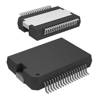
Type
On-state Resistance
Package
ISO1H816G
200mΩ
PG-DSO36
Datasheet
4
Revision 2.4, 2014-10-20
�ISOFACE™
ISO1H816G
Pin Configuration and Functionality
1
Pin Configuration and Functionality
1.1
Pin Configuration
Vbb
Pin
Symbol
1
N.C.
Not connected
2
VCC
Positive 3.3/5V logic supply
3
DIS
Output disable
4
CS
Chip select
5
SCLK
Serial Clock
6
SI
7
N.C.
Not connected
8
N.C.
Not connected
9
N.C.
Not connected
10
N.C.
Not connected
11
N.C.
Not connected
12
N.C.
Not connected
13
SO
Serial Data Output
14
DIAG
15
GNDCC
16
N.C.
Not connected
17
N.C.
Not connected
18
N.C.
Not connected
Figure 1
19
GNDbb
Output driver ground
.
20
N.C
21
OUT7
High-side output of channel 7
22
OUT7
High-side output of channel 7
23
OUT6
High-side output of channel 6
24
OUT6
High-side output of channel 6
25
OUT5
High-side output of channel 5
26
OUT5
High-side output of channel 5
27
OUT4
High-side output of channel 4
28
OUT4
High-side output of channel 4
29
OUT3
High-side output of channel 3
30
OUT3
High-side output of channel 3
31
OUT2
High-side output of channel 2
32
OUT2
High-side output of channel 2
33
OUT1
High-side output of channel 1
34
OUT1
High-side output of channel 1
35
OUT0
High-side output of channel 0
36
OUT0
High-side output of channel 0
TAB
Vbb
Datasheet
Function
N.C.
VCC
DIS
CS
SCLK
SI
N.C.
N.C.
N.C.
N.C.
N.C.
N.C.
SO
DIAG
GNDCC
N.C.
N.C.
N.C.
Serial Data input
Common diagnostic output
Input logic ground
1
2
3
4
5
6
7
8
9
10
11
12
13
14
15
16
17
18
TAB
TAB
36
35
34
33
32
31
30
29
28
27
26
25
24
23
22
21
20
19
OUT0
OUT0
OUT1
OUT1
OUT2
OUT2
OUT3
OUT3
OUT4
OUT4
OUT5
OUT5
OUT6
OUT6
OUT7
OUT7
N.C.
GNDbb
Vbb
Power SO-36 (430mil)
Not connected
Positive driver power supply voltage
5
Revision 2.4, 2014-10-20
�ISOFACE™
ISO1H816G
Pin Configuration and Functionality
1.2
Pin Functionality
GNDCC (Ground for VCC domain)
This pin acts as the ground reference for the input
interface that is supplied by VCC.
VCC (Positive 3.3/5V logic supply)
The VCC supplies the input interface that is
galvanically isolated from the output driver stage. The
input interface can be supplied with 3.3V / 5V.
GNDbb (Output driver ground domain)
This pin acts as the ground reference for the output
driver that is supplied by Vbb.
DIS (Output disable)
The high-side outputs OUT0...OUT7 can be
immediately switched off by means of the low active pin
DIS that is an asynchronous signal. The input registers
are also reset by the DIS signal. The output remains
switched off after low-high transient of DIS, till new data
is written into the input interface. Current Sink to
GNDCC
OUT0 ... OUT7 (High side output channel 0 ... 7)
The output high side channels are internally connected
to Vbb and controlled by the corresponding data input.
TAB (Vbb, Positive supply for output driver)
The heatslug is connected to the positive supply port of
the output interface.
CS (Chip select)
The system microcontroller selects the ISO1H816G by
means of the low active pin CS to activate the interface.
Current Source to VCC
SCLK (Serial shift clock)
SCLK (serial clock) is used to synchronize the data
transfer between the master and the ISO1H816G. Data
present at the SI pin are latched on the rising edge of
the serial clock input, while data at the SO pin is
updated after the falling edge of SCLK.
Current Source to VCC
SI (Serial data input)
This pin is used to transfer data into the device. Data is
latched on the rising edge of the serial clock. Current
Sink to GNDCC
SO (Serial data output)
SO can be connected to a serial input of a further IC to
build a daisy-chain configuration. It is only actvated if
CS is in low state, otherwise this output is in high
impedance state.
DIAG (Common diagnostic output)
The low active DIAG signal contains the OR-wired
information of the separated overtemperature detection
units for each channel.The output pin DIAG provides an
open drain functionality. A current source is also
connected to the pin DIAG. In normal operation the
signal DIAG is high. When overtemperature or Vbb
below ON-Limit is detected the signal DIAG changes to
low.
Datasheet
6
Revision 2.4, 2014-10-20
�Datasheet
7
DIAG
SO
SI
SCLK
CS
ISO1H816G
Serial
Input Interface
VCC
100µA
High-side Channel 7
Logic
Undervoltage
Charge Pump
Level shifter
Rectifier
Charge Pump
Level Shifter
Rectifier
Common
Diagnostic
Output
High-side Channel 0
Logic
to Logic
Channel 1 - 6
Undervoltage
Shutdown with
Restart
Overvoltage
Protection
Temperature Sensor
Overload Protection
Current Limitation
Limitation of Unclamped
Inductive Load
Vbb
Channel 1 ... 6
Gate
Protection
from
Temperature
Sensor
Channel 1 - 6
Temperature Sensor
Overload Protection
Current Limitation
Limitation of Unclamped
Inductive Load
Gate
Protection
Voltage
Source
OUT7
OUT6
OUT5
OUT4
OUT3
OUT2
OUT1
OUT0
GNDbb
Vbb
Blockdiagram
to Logic
Channel 1 - 6
Serial
to
Parallel
Figure 2
DIS
Logic
CT
Blockdiagram
GNDCC
Undervoltage
Shutdown with
Restart
2
Galvanic Isolation
VCC
ISOFACE™
ISO1H816G
Blockdiagram
Revision 2.4, 2014-10-20
�ISOFACE™
ISO1H816G
Functional Description
3
Functional Description
3.1
Introduction
3.3.2
The ISOFACE ISO1H816G includes 8 high-side power
switches that are controlled by means of the integrated
µC compatible SPI interface. The outputs
OUT0...OUT7 are controlled by the data of the serial
input SI. The IC can replace 8 optocouplers and the 8
high-side switches in conventional I/O-Applications as
a galvanic isolation is implemented by means of the
integrated coreless transformer technology. The µC
compatible interface allows a direct connection to the
ports of a microcontroller without the need for other
components. Each of the 8 high-side power switches is
protected
against
short to
Vbb,
overload,
overtemperature and against overvoltage by an active
zener clamp.
Each of the eight output stages has its own zener clamp
that causes a voltage limitation at the power transistor
when solenoid loads are switched off. VON is then
clamped to 47V (min.).
Vbb
VON
OUTx
GNDbb
Figure 3
Power Supply
Inductive and overvoltage output
clamp (each channel)
Energy is stored in the load inductance during an
inductive load switch-off.
The IC contains 2 galvanic isolated voltage domains
that are independent from each other. The input
interface is supplied at VCC and the output stage is
supplied at Vbb. The different voltage domains can be
switched on at different time. The output stage is only
enabled once the input stage enters a stable state.
3.3
EL = 1 ⁄ 2 × L × IL
2
Ebb
EAS
ELoad
Vbb
Output Stage
Dx
OUTx
L
Each channel contains a high-side vertical power FET
that is protected by embedded protection functions.
Vbb
GNDbb
RL
Output Stage Control
Figure 4
Each output is independently controlled by an output
latch and a common reset line via the pin DIS that
disables all eight outputs and resets the latches. Serial
data input (SI) is read on the rising edge of the serial
clock SCLK. A logic high input data bit turns the
respective output channel ON, a logic low data bit turns
it OFF. CS must be low whilst shifting all the serial data
into the device. A low-to-high transition of CS transfers
the serial data input bits to the output buffer.
Datasheet
EL
ZL
The continuous current for each channel is 1.2A (all
channels ON).
3.3.1
Vbb
Vz
The diagnostic logic on the power chip recognizes the
overtemperature information of each power transistor
The information is send via the internal coreless
transformer to the pin DIAG at the input interface.
3.2
Power Transistor Overvoltage
Protection
ER
Inductive load switch-off energy
dissipation (each channel)
While demagnetizing the load inductance, the energy
dissipation in the DMOS is
E AS = E bb + E L – E R = V ON ( CL ) × i L ( t )dt
with an approximate solution for RL > 0Ω::
IL × L
IL × RL ⎞
E AS = ---------------- × ( V bb + V ON ( CL ) ) × ln ⎛⎝ 1 + -----------------------2 × RL
V ON ( CL ) ⎠
8
Revision 2.4, 2014-10-20
�ISOFACE™
ISO1H816G
Functional Description
3.3.3
Power Transistor Overcurrent
Protection
IN
The outputs are provided with a current limitation that
enters a repetitive switched mode after an initial peak
current has been exceeded. The initial peak short
circuit current limit is set to IL(SCp) at Tj = 125°C. During
the repetitive short circuit the current limit is set to IL(SCr).
If this operation leads to an overtemperature condition,
a second protection level (Tj > 135°C) will change the
output into a low duty cycle PWM (selective thermal
shutdown with restart) to prevent critical chip
temperatures.
t
VOUT
Normal
operation
IL
Output short to GND
IL(SCp)
t
IL(SCr)
t
DIAG
IN
t
VOUT
t
TJ
t
DIAG
t
Short circuit in on-state, shut down
down by overtemperature, restart by
cooling
3.4
Common Diagnostic Output
The overtemperature detection information are ORwired in the common diagnostic output block. The
information is send via the integrated coreless
transformer to the input interface. In addition Vbb
undervoltage is indicated at the DIAG output.
t
Figure 5
Figure 7
The output stage at pin DIAG has an open drain
functionality combined with a current source.
Overtemperature detection
The following figures show the timing for a turn on into
short circuit and a short circuit in on-state. Heating up
of the chip may require several milliseconds,
depending on external conditions.
VCC
100µA
DIAG
IN
CT
Common
Diagnostic
Output
t
VOUT
Output short to GND
IL
IL(SCp)
t
IL(SCr)
Figure 8
DIAG
Common diagnostic output
t
t
Figure 6
Datasheet
Turn on into short circuit, shut down by
overtemperature, restart by cooling
9
Revision 2.4, 2014-10-20
�ISOFACE™
ISO1H816G
Functional Description
3.5
Serial Interface
SI - Serial input. Serial data bits are shifted in at this pin,
the most significant bit first. SI information is read in on
the rising edge of the SCLK. Input data is latched in the
shift register and then transferred to the control buffer
of the output stages.
The ISO1H816G contains a serial interface that can be
directly controlled by the microcontroller output ports.
3.5.1
SPI Signal Description
SO - Serial output. SO is in a high impedance state until
the CS pin goes to a logic low state. The data of the
internal shift register are shifted out serially at this pin.
The most significant bit will appear at first. The further
bits will appear following the falling edge of SCLK.
CS - Chip select. The system microcontroller selects
the ISO1H816G by means of the CS pin. Whenever the
pin is in a logic low state, data can be transferred from
the µC.
CS High to low transition:
•Serial input data can be clocked in from then on
3.5.2
SPI Bus Concepts
3.5.2.1
Independent Individual Control
Each IC with a SPI is controlled individually and
independently by an SPI master, as in a directional
point-to-point communication.The port requirements
for this topology are the greatest, because for each
controlled IC an individual SPI at the µC is needed
(SCLK, CS, SI). All ICs can be
addressed
simultaneously with the full SPI bandwidth.
•SO changes from high impendance state to logic high
or low state corresponding to the SO bit-state
CS Low to high transition:
•Transfer of SI bits from shift register into output
buffers, if number of clock signals was an integer
multiple of 8
SPI 1
•SO changes from the SO bit-state to high impendance
state
CLK
Tx a1
Tx a2
SCLK
CS
SI
Output lines
SO
SPI - Interface
IC1
To avoid any false clocking the serial input pin SCLK
should be logic high state during high-to-low transition
of CS. When CS is in a logic high state, any signals at
the SCLK and SI pins are ignored and SO is forced into
a high impedance state. The integrated modulo counter
that counts the number of clocks avoids the take over
of invalid commands caused by a spike on the clock
line or wrong number of clock cycles. A command is
only taken over, if after the low-to-high transition of the
CS signal the number of counted clock cycles is
recognized as a multiple of 8.
SPI n
SCLK
CS
SI
Output lines
SO
SPI - Interface
µC
SCLK - Serial clock. The system clock pin clocks the
internal shift register of the ISO1H816G. The serial
input (SI) accepts data into the input shift register on the
rising edge of SCLK while the serial output (SO) shifts
the output information out of the shift register on the
falling edge of the serial clock. It is essential that the
SCLK pin is in a logic high state whenever chip select
CS makes any transition. The number of clock pulses
will be counted during a chip select cycle. The received
data will only be accepted, if exactly an integer multiple
of 8 clock pulses were counted during CS is active.
Datasheet
CLK
Tx n1
Tx n2
ICn
Number of adressed ICs = n
Number of necessary control and data ports = 3 n
Individual ICs are adressed by the chip select
Figure 9
10
Individual independent control of each
IC with SPI
Revision 2.4, 2014-10-20
�ISOFACE™
ISO1H816G
Functional Description
3.5.2.2
Daisy-chain Configuration
3.6
The connection of different ICs and a µC as shown in
Fig. 10 is called a daisy-chain. For this type of bustopology only one SPI interface of the µC for two or
more ICs is needed. All ICs share the same clock and
chip select port of the SPI master. That is all ICs are
active and addressed simultaneously. The data out of
the µC is connected to the SI of the first IC in the line.
Each SO of an IC is connected to the SI of the next IC
in the line.
SPI 1
CLK
Tx a1
Tx a2
SCLK
CS
SI
SO
Transmission Failure Detection
There is a failure detection unit integrated to ensure
also a stable functionality during the integrated
coreless transformer transmission. This unit decides
whether the transmitted data is valid or not. If four times
serial data coming from the internal registers is not
accepted the output stages are switched off until the
next valid data is received.
Output lines
SPI - Interface
IC1
SCLK
CS
SI
Output lines
SPI - Interface
µC
ICn
Number of adressed ICs = n
Number of necessary control and data ports = 3
All ICs are adressed by the common chip select
Figure 10
SPI bus all ICs in a “daisy chain”
configuration
The µC feeds the data bits into the SI of IC1 (first IC in
the chain). The bits coming from the SO of IC1 are
directly shifted into the SI of the next IC. As long as the
chip select is inactive (logic high) all the IC SPIs ignore
the clock (SCLK) and input signals (SI) and all outputs
(SO) are in tristate. As long as the chip select is active
the SPI register works as a simple shift register. With
each clock signal one input is shifted into the SPI
register (SI), each bit in the shift register moves one
position further within the register, and the last bit in the
SPI shift register is shifted out of SO. This is continued
as long as the chip select is active (logic low) and clock
signals are applied. The data is then only taken over to
the output buffers of each IC when the CS signal
changes to high from low and recognized as valid data
by the internal modulo counter.
Datasheet
11
Revision 2.4, 2014-10-20
�ISOFACE™
ISO1H816G
Functional Description
3.7
Serial Interface Timing
Chipselect active
CS
SCLK
n+7
SI
SO
Figure 11
n+5
n+4
n+3
n+2
n+1
n
n-1
n-2
n-3
n-4
n-5
n-6
n-7
Serial interface
tp(SCLK)
tCSS
tCSH
≈
CS
n
n+6
tCSD
tSU
SI
Figure 12
≈ ≈ ≈
SCLK
tHD
MSB In
LSB In
Serial input timing diagram
≈≈
CS
SCLK
t SODIS
SO
Figure 13
Datasheet
≈ ≈
tVALID
MSB Out
LSB Out
Serial output timing diagram
12
Revision 2.4, 2014-10-20
�ISOFACE™
ISO1H816G
Electrical Characteristics
4
Electrical Characteristics
Note: All voltages at pins 2 to 14 are measured with respect to ground GNDCC (pin 15). All voltages at pin 20 to
pin 36 and TAB are measured with respect to ground GNDbb (pin 19). The voltage levels are valid if other
ratings are not violated. The two voltage domains VCC ,GNDCC and Vbb ,GNDbb are internally galvanically
isolated.
4.1
Absolute Maximum Ratings
Note: Absolute maximum ratings are defined as ratings, which when being exceeded may lead to destruction of
the integrated circuit. For the same reason make sure, that any capacitor that will be connected to pin 2
(VCC) and TAB (Vbb) is discharged before assembling the application circuit. Supply voltages higher than
Vbb(AZ) require an external current limit for the GNDbb pin, e.g. with a 15Ω resistor in GNDbb connection.
Operating at absolute maximum ratings can lead to a reduced lifetime.
Parameter
at Tj = -40 ... 135°C, unless otherwise specified
Symbol
Supply voltage input interface (VCC)
VCC
Limit Values
Unit
min.
max.
-0.5
6.5
1)
45
V
Supply voltage output interface (Vbb)
Vbb
-1
Continuos voltage at pin SI
VSI
-0.5
6.5
Continuos voltage at pin CS
VCS
-0.5
6.5
Continuos voltage at pin SCLK
VSCLK
-0.5
6.5
Continuos voltage at pin DIS
VDIS
-0.5
6.5
Continuos voltage at pin SO
VSO
-0.5
6.5
Continuos voltage at pin DIAG
VDIAG
-0.5
6.5
Load current (short-circuit current)
IL
---
self limited
IGNDbb
-1.6
---
Operating Temperature
Tj
-25
internal limited °C
Extended Operation Temperature
Tj
-40
internal limited
Storage Temperature
Tstg
-50
150
Ptot
---
3.3
Reverse current through GNDbb
Power Dissipation
1)
2)
3)
Inductive load switch-off energy dissipation single
pulse, Tj = 125°C, IL = 1.2A
one channel active
all channel simultaneously active (each channel)
EAS
Load dump protection3) VloadDump4)=VA + VS
VIN = low or high
td = 400ms, RI = 2W, RL = 27W, VA = 13.5V
td = 350ms, RI = 2W, RL = 57W, VA = 27V
VLoaddump
Electrostatic discharge voltage (Human Body Model)
according to JESD22-A114-B
VESD
Electrostatic discharge voltage (Charge Device Model)
according to ESD STM5.3.1 - 1999
VESD
Continuos reverse drain current1)3), each channel
IS
A
W
J
---
10
1
V
-----
90
117
kV
2
kV
1
---
4
A
1) defined by Ptot
2) Device on 50mm*50mm*1.5mm epoxy PCB FR4 with 6cm² (one layer, 70µm thick) copper area for drain connection. PCB
is vertical without blown air.
3) not subject to production test, specified by design
4) VLoaddump is setup without the DUT connected to the generator per ISO7637-1 and DIN40839
Datasheet
13
Revision 2.4, 2014-10-20
�ISOFACE™
ISO1H816G
Electrical Characteristics
4.2
Thermal Characteristics
Parameter
Symbol
at Tj = -25 ... 125°C, Vbb=15...30V, VCC= 3.0...5.5V,
unless otherwise specified
Limit Values
min.
Unit Test Condition
typ.
max.
Thermal resistance junction - case
RthJC
---
---
1.5
Thermal resistance @ min. footprint
Rth(JA)
---
---
50
Thermal resistance @ 6cm² cooling area1)
Rth(JA)
---
---
38
K/W
1) Device on 50mm*50mm*1.5mm epoxy PCB FR4 with 6cm² (one layer, 70µm thick) copper area for drain connection. PCB
is vertical without blown air.
4.3
Load Switching Capabilities and Characteristics
Parameter
Symbol
at Tj = -25 ... 125°C, Vbb=15...30V, VCC= 3.0...5.5V,
unless otherwise specified
On-state resistance, IL = 0.5A, each channel
Tj = 25°C
Tj = 125°C
two parallel channels, Tj = 25°C:1)
four parallel channels, Tj = 25°C:1)
Nominal load current
Device on PCB 38K/W, Ta = 85°C, Tj < 125°C
one channel:1)
two parallel channels:1)
four parallel channels:1)
Limit Values
Unit
min.
typ.
max.
-----
150
270
75
38
200
320
100
50
Test Condition
mΩ
RON
A
IL(NOM)
1.4
2.2
4.4
Turn-on time to 90% VOUT2)
RL = 47Ω, VDx = 0 to 5V
ton
---
64
120
Turn-off time to 10% VOUT1)
RL = 47Ω, VDx = 5 to 0V
toff
---
89
170
Slew rate on 10 to 30% VOUT
RL = 47Ω, Vbb = 15V
dV/dton
---
1
2
Slew rate off 70 to 40% VOUT
RL = 47Ω, Vbb = 15V
-dV/dtoff
---
1
2
µs
V/µs
1) not subject to production test, specified by design
2) The turn-on and turn-off time includes the switching time of the high-side switch and the transmission time via the coreless
transformer in normal operating mode. During a failure on the coreless transformer transmission turn-on or turn-off time
can increase by up to 50µs.
Datasheet
14
Revision 2.4, 2014-10-20
�ISOFACE™
ISO1H816G
Electrical Characteristics
4.4
Operating Parameters
Parameter
at Tj = -25 ... 125°C, Vbb=15...30V, VCC=
3.0...5.5V, unless otherwise specified
Symbol
Common mode transient immunity1)
Magnetic field immunity1)
Voltage domain Vbb
(Output interface)
Limit Values
Unit
Test Condition
min.
typ.
max.
ΔVISO/dt
-25
-
25
HIM
100
Operating voltage
Vbb
11
---
35
Undervoltage shutdown
Vbb(under)
7
---
10.5
Undervoltage restart
Vbb(u_rst)
---
---
11
Undervoltage hysteresis
ΔVbb(under)
---
0.5
---
Undervoltage current
Ibb(uvlo)
---
1
2.5
mA
Vbb < 7V
Operating current
IGNDL
---
10
14
mA
All Channels
ON - no load
Leakage output current
(included in Ibb(off))
VDx = low, each channel
IL(off)
---
5
30
µA
Voltage domain VCC Operating voltage
(Input interface)
Undervoltage shutdown
VCC
3.0
---
5.5
V
VCC(under)
2.5
---
2.9
Undervoltage restart
VCC(u_rst)
---
---
3
Undervoltage hysteresis
ΔVCC(under)
---
0.1
---
Undervoltage current
ICC(uvlo)
---
1
2
mA
Operating current
ICC(on)
---
4.5
6
mA
kV/µs ΔVISO = 500V
A/m
IEC61000-4-8
V
Vcc < 2.5V
1) not subject to production test
Datasheet
15
Revision 2.4, 2014-10-20
�ISOFACE™
ISO1H816G
Electrical Characteristics
4.5
Output Protection Functions
Parameter1)
Symbol
at Tj = -25 ... 125°C, Vbb=15...30V, VCC=3.0...5.5V,
unless otherwise specified
Initial peak short circuit current limit, each channel IL(SCp)
Tj = -25°C, Vbb = 30V, tm = 700µs
Tj = 25°C
Tj = 125°C
two parallel channels:2)
four parallel channels:2)
Limit Values
Unit Test Condition
min.
typ.
max.
----1.4
--3.0
---
4.5
-----
A
twice the current of one channel
four times the current of one channel
---
Repetitive short circuit current limit
Tj = Tjt (see timing diagrams)
each channel:2) IL(SCr)
two parallel channels:2)
four parallel channels:2)
---
Output clamp (inductive load switch off)3)
at VOUT = Vbb - VON(CL)
VON(CL)
47
53
60
Overvoltage protection
Vbb(AZ)
47
---
---
Tjt
135
---
---
°C
---
10
---
K
2) 4)
Thermal overload trip temperature
Thermal hysteresis
2)
ΔTjt
2.2
2.2
2.2
V
1) Integrated protection functions are designed to prevent IC destruction under fault conditions described in the data sheet.
Fault conditions are considered as “outside” normal operating range. Protection functions are not designed for continuos
repetitive operation.
2) not subject to production test, specified by design
3) If channels are connected in parallel, output clamp is usually accomplished by the channel with the lowest VON(CL)
4) Higher operating temperature at normal function for each channel available
4.6
Diagnostic Characteristics at pin DIAG
Symbol
Parameter
at Tj = -25 ... 125°C, Vbb=15...30V, VCC=3.0...5.5V,
unless otherwise specified
Common diagnostic sink current
(overtemperature of any channel) Tj = 135°C
Idiagsink
Common diagnostic source current
Idiagsource
Datasheet
16
Limit Values
min.
typ.
Unit Test Condition
max.
5
100
mA
VDIAGON < 0.25 x
VCC
µA
Revision 2.4, 2014-10-20
�ISOFACE™
ISO1H816G
Electrical Characteristics
4.7
Input Interface
Parameter
Symbol
at Tj = -25 ... 125°C, Vbb=15...30V, VCC= 3.0...5.5V,
unless otherwise specified
Limit Values
Unit Test Condition
min.
typ.
max.
Input low state voltage
(SI, DIS, CS, SCLK)
VIL
-0.3
---
0.3 x
VCC
Input high state voltage
(SI, DIS, CS, SCLK)
VIH
0.7 x
VCC
---
VCC+
0.3
Input voltage hysteresis
(SI, DIS, CS, SCLK)
VIHys
Output low state voltage
(SO)
VOL
-0.3
---
0.25 x V
VCC
Output high state voltage
(SO)
VOH
0.75 x
VCC
---
VCC+
0.3
Input pull down current
(SI , DIS)
IIdown
100
Input pull up current
(CS, SCLK)
-IIup
100
100
V
mV
CL < 50pF,
RL > 10kΩ
µA
Output disable time (transition DIS to logic low)1)2) tDIS
Normal operation
Turn-off time to 10% VOUT
RL = 47Ω
---
85
170
Output disable time (transition DIS to logic low)1)2)3) tDIS
Disturbed operation
Turn-off time to 10% VOUT
RL = 47Ω
---
---
230
µs
1) The time includes the turn-on/off time of the high-side switch and the transmission time via the coreless transformer.
2) If Pin DIS is set to low the outputs are set to low; after DIS set to high a new write cycle is necessary to set the output again.
3) The parameter is not subject to production test - verified by design/characterization
Datasheet
17
Revision 2.4, 2014-10-20
�ISOFACE™
ISO1H816G
Electrical Characteristics
4.8
SPI Timing
Parameter
Symbol
at Tj = -25 ... 125°C, Vbb=15...30V, VCC= 3.0...5.5V,
unless otherwise specified
Limit Values
min.
Unit Test Condition
typ.
max.
Serial clock frequency
fSCLK
DC
---
20
MHz
Serial clock period (1/fclk)
tp(SLCK)
50
---
---
ns
CS Setup time (falling edge of CS to falling edge of tCSS
SCLK)
5
---
---
CS Hold time (rising edge of SCLK to rising edge tCSH
of CS)
10
---
---
CS Disable time (CS high time between two
accesses)
10
---
---
Data setup time (required time SI to rising edge of tSU
SCLK)
6
---
---
Data hold time (falling edge of SCLK to SI)
tHD
6
---
---
SO Output valid time
CL = 50pF
tVALID
---
---
20
tCSD
SO Output disable time
tSODIS
Delay to next CS cycle for multiple device
synchronization1)
tCSDMD
20
Input to output data transmission jitter
tIOJ
8
20
ns
µs
2)
2)
20
1) necessary CS delay time to ensure a proper data update for multiple devices
2) not subject to production test, specified by design
4.9
Reverse Voltage
Parameter
Symbol
at Tj = -25 ... 125°C, Vbb=15...30V, VCC= 3.0...5.5V,
unless otherwise specified
Reverse voltage1)2)RGND = 0 Ω
RGND = 150 Ω
-Vbb
Diode forward on voltage
IF = 1.25A, VDx = low, each channel
-VON
Limit Values
Unit Test Condition
min.
typ.
max.
-----
-----
1
45
---
---
1.2
V
1) defined by Ptot
2) not subject to production test, specified by design
Datasheet
18
Revision 2.4, 2014-10-20
�ISOFACE™
ISO1H816G
Electrical Characteristics
4.10
Isolation and Safety-Related Specification
Parameter
Value
Unit
Conditions
Rated dielectric isolation voltage VISO
500
VAC
1 - minute duration1)
Short term temporary overvoltage
1250
V
5s acc. DIN EN60664-1 1)
Minimum external air gap (clearance)
2.6
mm
shortest distance through air.
Minimum external tracking (creepage)
2.6
mm
shortest distance path along body.
1) not subject to production test, verified by characterization; Production Test with 1100V, 100ms duration
4.11
Reliability
For Qualification Report please contact your local Infineon Technologies office!
Datasheet
19
Revision 2.4, 2014-10-20
�ISOFACE™
ISO1H816G
Electrical Characteristics
Datasheet
20
Revision 2.4, 2014-10-20
�ISOFACE™
ISO1H816G
Electrical Characteristics
Datasheet
21
Revision 2.4, 2014-10-20
�ISOFACE™
ISO1H816G
Package Outlines
Package Outlines
0.65
0.25 +0.13
15.74 ±0.1
(Heatslug)
+0.07
-0.02
B
2.8
6.3
0.1 C
(Mold)
5˚ ±3˚
0.25
0 +0.1
1.1 ±0.1
11 ±0.15 1)
1.3
(Plastic Dual Small
Outline Package)
3.25 ±0.1
PG-DSO-36
3.5 MAX.
5
Heatslug
0.95 ±0.15
36x
0.25 M A B C
14.2 ±0.3
0.25 B
19
19
1
18
10
36
5.9 ±0.1
(Metal)
36
3.2 ±0.1
(Metal)
Bottom View
Index Marking
1 x 45˚
15.9 ±0.1 1)
(Mold)
1)
Figure 14
Datasheet
A
13.7 -0.2
(Metal)
Does not include plastic or metal protrusion of 0.15 max. per side
1
Heatslug
gps09181_1
PG-DSO36
22
Revision 2.4, 2014-10-20
�w w w . i n f i n e o n . c o m
Published by Infineon Technologies AG
�