ITS4200S-ME-N
Smart High-Side NMOS-Power Switch
Data Sheet
Rev 1.0, 2012-09-01
Standard Power
�Smart High-Side NMOS-Power Switch
1
ITS4200S-ME-N
Overview
Features
•
•
•
•
•
•
•
•
•
•
•
•
•
•
CMOS compatible input
Switching all types of resistive, inductive and capacitive loads
Fast demagnetization of inductive loads
Very low standby current
Optimized Electromagnetic Compatibility
Overload protection
Current limitation
Short circuit protection
Thermal shutdown with restart
Overvoltage protection (including load dump)
Reverse battery protection with external resistor
Loss of GND and loss of Vbb protection
Electrostatic Discharge Protection (ESD)
Green Product (RoHS compliant)
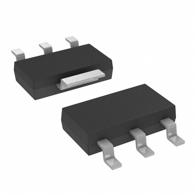
SOT-223-4
ITS4200S-ME-N is not qualified and manufactured according to the requirements of Infineon Technologies with
regards to automotive and/or transportation applications.
Description
The ITS4200S-ME-N is a protected single channel Smart High-Side NMOS-Power Switch in a SOT-223-4
package with charge pump and CMOS compatible input. The device is monolithically integrated in Smart
technology.
Product Summary
Overvoltage protection VSAZ min= 41V
Operating voltage range: 5V ≤VS≤ 34V
On-state resistance RDSON typ = 160mΩ
Nominal load current ILNOM = 0.7A
Operating Temperature range: Tj = -40°C to 125°C
Standby Current: ISSTB= 25µA
Application
•
•
•
•
All types of resistive, inductive and capacitive loads
Power switch for 12V and 24V DC applications with CMOS compatible control interface
Driver for electromagnetic relays
Power managment for high-side-switching with low current consumption in OFF-mode
Type
Package
Marking
ITS4200S-ME-N
SOT-223-4
I200SN
Data Sheet
2
Rev 1.0, 2012-09-01
�ITS4200S-ME-N
Block Diagram and Terms
2
Block Diagram and Terms
ITS4200S-ME-N
VS
4
Bias
Supervision
IN
Overvoltage
Protection
Current
Limiter
Logic
Gate
Control
Circuit
3
ESD
Protection
Temperature
Sensor
OUT
1
2
GND
Figure 1
Block diagram
Voltage- and Current-Definitions:
Switching Times and Slew Rate Definitions:
VIN
H
ITS4200S-ME-N
4
Bias
Supervision
Overvoltage
Protection
L
VS
IS
VOUT
t
+VS
Current
Limiter
VDS
90%
IN
I IN
3
V FD S
70%
Gate
Control
Circuit
Logic
ESD
Protection
SROFF
40%
30%
SRON
10%
IOUT
IL
V ST
GND
RL
V O UT
2
tON
t
tOFF
IL
V IN
1
OUT
0
VS
Temperature
Sensor
0
OFF
ON
OFF
t
GND
Figure 2
Data Sheet
Terms - parameter definition
3
Rev 1.0, 2012-09-01
�ITS4200S-ME-N
Pin Configuration
3
Pin Configuration
3.1
Pin Assignment
4
1
2
Figure 3
Pin configuration top view, SOT-223-4
3.2
Pin Definitions and Functions
3
Pin
Symbol
Function
1
OUT
Output to the load
2
GND
Logic ground
3
IN
Input, controles the power switch; the powerswitch is ON when high
4
VS
Supply voltage (design the wiring for the maximum short circuit current and also
for low thermal resistance)
Data Sheet
4
Rev 1.0, 2012-09-01
�ITS4200S-ME-N
General Product Characteristics
4
General Product Characteristics
4.1
Absolute Maximum Ratings
Table 1
Absolute maximum ratings 2) at Tj = 25°C unless otherwise specified. Currents flowing into the
device unless otherwise specified in chapter “Block Diagram and Terms”
Parameter
Symbol
Values
Min.
Typ.
Max.
Unit Note /
Test Condition
Number
VS
–
–
40
V
4.1.1
IOUT
self
limited
A
4.1.2
VIN
IIN
-5
–
VS
V
4.1.3
-5
–
5
mA
4.1.4
Tj
Tstg
-40
–
125
°C
4.1.5
-55
–
125
°C
4.1.6
P tot
–
–
1.4
W
4.1.7
EAS
–
–
500
mJ
single pulse
4.1.8
VESD
VESD
-1
–
1
kV
HBM3)
4.1.9
kV
3)
Supply voltage VS
Voltage
Output stage OUT
Output Current; (Short circuit
current see electrical
characteristics)
Input IN
Voltage
Current
Temperatures
Junction Temperature
Storage Temperature
Power dissipation
Ta = 25 °C1)
Inductive load switch-off energy dissipation
Tj = 125 °C; VS=13.5V; IL= 0.5A2)
ESD Susceptibility
ESD susceptibility (input pin)
ESD susceptibility (all other pins)
-2
–
2
HBM
4.1.10
1) Device on 50mm*50mm*1.5mm epoxy PCB FR4 with 6 cm2 (one layer, 70mm thick) copper area for Vbb connection. PCB
is vertical without blown air
2) Not subject to production test, specified by design
3) ESD susceptibility HBM according to EIA/JESD 22-A 114.
Note: Exposure to absolute maximum rating conditions for extended periods may affect device reliability.
Integrated protection functions are designed to prevent IC destruction under fault conditions described in the
data sheet. Fault conditions are considered as “outside” the normal operating range. Protection functions
are neither designed for continuous nor repetitive operation.
Data Sheet
5
Rev 1.0, 2012-09-01
�ITS4200S-ME-N
General Product Characteristics
4.2
Functional Range
Table 2
Functional Range
Parameter
Symbol
Nominal Operating Voltage
VS
VIN
Continuous Input Voltage
Values
Unit
Note /
Test Condition
Number
VS increasing
4.2.1
Min.
Typ.
Max.
5
–
34
V
-3
–
VS
V
4.2.2
Note: Within the functional range the IC operates as described in the circuit description. The electrical
characteristics are specified within the conditions given in the related electrical characteristics table.
4.3
Thermal Resistance
This thermal data was generated in accordance to JEDEC JESD51 standards.
More information on www.jedec.org
Table 3
Thermal Resistance1)
Parameter
Symbol
Values
Unit
Min.
Typ.
Max.
Note /
Test Condition
Number
Thermal Resistance Junction to pin5
Rthj-pin5
–
35.0
–
K/W
Thermal Resistance Junction to Ambient - 1s0p,
minimal footprint
RthJA_1s0p
–
120.0
–
K/W
2)
4.3.2
Thermal Resistance Junction to Ambient - 1s0p,
300mm2
RthJA_1s0p_30 –
69.3
–
K/W
3)
4.3.3
Thermal Resistance Junction to Ambient - 1s0p,
600mm2
RthJA_1s0p_60 –
61.6
–
K/W
4)
4.3.4
Thermal Resistance Junction to Ambient - 2s2p
RthJA_2s2p
–
55.5
–
K/W
5)
4.3.5
Thermal Resistance Junction to Ambient with
thermal vias - 2s2p
RthJA_2s2p
–
48.3
–
K/W
6)
4.3.6
4.3.1
0mm
0mm
1) Not subject to production test, specified by design
2) Specified RthJA value is according to Jedec JESD51-3 at natural convection on FR4 1s0p board, footprint; the Product
(Chip+Package) was simulated on a 76.2 x 114.3 x 1.5 mm board with 1x 70µm Cu.
3) Specified RthJA value is according to Jedec JESD51-3 at natural convection on FR4 1s0p board, Cu, 300mm2; the Product
(Chip+Package) was simulated on a 76.2 x 114.3 x 1.5 mm board with 1x 70µm Cu.
4) Specified RthJA value is according to Jedec JESD51-3 at natural convection on FR4 1s0p board, 600mm2; the Product
(Chip+Package) was simulated on a 76.2 x 114.3 x 1.5 mm board with 1x 70µm Cu.
5) Specified RthJA value is according to Jedec JESD51-2,-5,-7 at natural convection on FR4 2s2p board; the Product
(Chip+Package) was simulated on a 76.2 x 114.3 x 1.5 mm board with 2 inner copper layers (2 x 70µm Cu, 2 x 35µm Cu).
Data Sheet
6
Rev 1.0, 2012-09-01
�ITS4200S-ME-N
General Product Characteristics
6) Specified RthJA value is according to Jedec JESD51-2,-5,-7 at natural convection on FR4 2s2p board with two thermal vias;
the Product (Chip+Package) was simulated on a 76.2 x 114.3 x 1.5 mm board with 2 inner copper layers (2 x 70µm Cu, 2
x 35µm Cu. The diameter of the two vias are equal 0.3mm and have a plating of 25um with a copper heatsink area of 3mm
x 2mm). JEDEC51-7: The two plated-through hole vias should have a solder land of no less than 1.25 mm diameter with
a drill hole of no less than 0.85 mm diameter.
Data Sheet
7
Rev 1.0, 2012-09-01
�ITS4200S-ME-N
Electrical Characteristics
5
Electrical Characteristics
Table 4
VS = 13.5V; Tj = 25°C; all voltages with respect to ground, currents flowing into the device unless otherwise specified in chapter “Block Diagram and Terms”. Typical values at Vs = 13.5V,
Tj = 25°C
Parameter
Symbol
Values
Min.
Typ.
Max.
Unit
Note /
Test Condition
Number
5.0.1
5.0.3
Powerstage
NMOS ON Resistance
RDSON
–
160
200
mΩ
NMOS ON Resistance
RDSON
–
–
400
mΩ
Nominal Load Current;
device on PCB 1)
ILNOM
0.7
–
–
A
IOUT= 0.5A;
Tj = 25°C;
VIN= 5V
IOUT= 0.5A;
Tj = 125°C;
VIN= 5V
Tpin5 = 85°C
Turn ON Time(to 90% of Vout);
L to H transition of VIN
tON
–
60
100
µs
VS=13.5V; RL = 24Ω
5.0.4
Turn OFF Time (to 10% of Vout);
H to L transition of VIN
tOFF
–
60
150
µs
VS=13.5V; RL = 24Ω
5.0.5
ON-Slew Rate (10 to 30% of Vout);
L to H transition of VIN
SRON
–
2
4
V /µs VS=13.5V; RL = 24Ω
5.0.6
OFF-Slew Rate; dVOUT / dtON
(70 to 40% of Vout);
H to L transition of VIN
SROFF
–
2
4
V /µs VS=13.5V; RL = 24Ω
5.0.7
5.0
V
VS decreasing
5.0.8
5.0.2
Timings of Power Stages2)
Under voltage lockout (charge pump start-stop-restart)
Supply undervoltage;
charge pump stop voltage
VSUV
Supply startup voltage
VSSU
–
–
6.5
V
VS increasing
Supply startup voltage
VSSU
–
–
7.0
V
VS increasing
3.5
–
Tj = -40°C to 125°C
5.0.9
Tj = -40°C to 25°C
5.0.10
Tj = 125°C
Supply startup voltage;
Charge pump restart voltage
VSSCHP
–
5.6
7.0
V
Undervoltage hysteresis;
VUVHYS=VSSU-VSUV
VUVHYS
–
0.3
–
V
VSOV
34
–
42
V
VS increasing
5.0.11
5.0.12
Over voltage lockout
Overvoltage shutdown thresthold
VS decreasing
5.0.13
Tj = -40°C to 125°C
Overvoltage restart thresthold
VSOVRS
33
–
V
VS decreasing
5.0.14
Tj = -40°C to 125°C
Overvoltage
hysteresis;VOVHYS=VSOCSD-VSOVRS
VOVHYS
–
0.7
–
V
5.0.15
Current consumption
Data Sheet
8
Rev 1.0, 2012-09-01
�ITS4200S-ME-N
Electrical Characteristics
Table 4
VS = 13.5V; Tj = 25°C; all voltages with respect to ground, currents flowing into the device unless otherwise specified in chapter “Block Diagram and Terms”. Typical values at Vs = 13.5V,
Tj = 25°C
Parameter
Symbol
Values
Unit
Note /
Test Condition
Number
Min.
Typ.
Max.
Operating current
–
1.0
Standby current
IGND
ISSTB
1.6
mA
5.0.16
10
25
µA
VIN= 5V
VIN= 0V; VOUT= 0V;
–
Output leakage current
IOUTLK
–
2
5
µA
5.0.17
Tj = -40°C to 125°C
VIN= 0V; VOUT= 0V;
5.0.18
Tj = -40°C to 25°C
–
–
7
µA
VIN= 0V; VOUT= 0V;
Tj = 125°C
5.0.19
Initial peak short circuit current limit ILSCP
0.7
1.5
2.0
A
Tj = 25°C;VS = 20V;
VIN = 5.0V
5.0.20
Initial peak short circuit current limit ILSCP
0.7
–
2.4
A
Tj = -40°C to 125°C;
VS = 20V;VIN = 5.0V
5.0.21
Output clamp at VOUT = VS - VDSCL
(inductive load switch off)
VDSCL
41
47
–
V
IS = 4mA
5.0.22
Overvoltage protection
VSAZ
41
–
–
V
IS = 4mA;
Tj = -40°C to 125°C
5.0.23
Thermal overload
trip temperature
TjTrip
150
–
–
°C
–
5.0.24
Thermal hysteresis
THYS
–
10
–
K
–
5.0.25
–
V
–
5.0.26
5.0.27
Output leakage current
IOUTLK
Protection functions 3)
Reverse Battery
4)
Continuous reverse battery voltage VSREV
- 30
Input interface; pin IN
3.5
–
–
V
Tj = -40°C to 125°C
–
–
1.5
V
Tj = -40°C to 125°C
5.0.28
–
0.5
–
V
–
5.0.29
Off state input current
VINON
VINOFF
VINHYS
IINOFF
10
–
60
µA
VIN = 1.2V;
5.0.30
On state input current
IINON
10
–
100
µA
VIN = 3V to VS;
Input turn-ON threshold voltage
Input turn-OFF threshold voltage
Input threshold hysteresis
Tj = -40°C to 125°C
5.0.31
Tj = -40°C to 125°C
Input resistance
RIN
1.5
2.8
3.5
kΩ
–
5.0.32
1) Device on 50mm x 50mm x 1,5mm epoxy FR4 PCB with 6cm² (one layer copper 70um thick) copper area for supply voltage
connection. PCB in vertical position without blown air.
2) Timing values only with high slewrate input signal; otherwise slower.
3) Integrated protection functions are designed to prevent IC destruction under fault conditions described in the data sheet.
Fault conditions are considered as “outside” normal operating range. Protection functions are not designed for continuous
repetitive operation.
4) Requires a 150W resistor in GND connection. The reverse load current trough the intrinsic drain-source diode of the
power-MOS has to be limited by the connected load. Power dissipation is higher compared to normal operation due to the
votage drop across the drain-source diode. The temperature protection is not functional during reverse current operation!
Input current has to be limited (see max ratings).
Data Sheet
9
Rev 1.0, 2012-09-01
�ITS4200S-ME-N
Typical Performance Graphs
6
Typical Performance Graphs
Maximal allowable Power Dissipation Ptot versus
Ambient and Soldering Point TemperatureTa; TSP
Initial Peak Short Circuit Current Limit ILSCP versus
Drain-Source Voltage VDS
2
18
Tsp
TA
1.8
16
1.6
14
1.4
12
ILSC [A]
Ptot [W]
1.2
10
8
1
0.8
6
0.6
4
0.4
2
0.2
0
0
Tj=−40°C
Tj=25°C
Tj=125°C
25
125
0
2
4
Tj [°C]
On-Resistance RDSONversus
Junction Temperature Tj
6
8
VON [V]
10
12
14
On-Resistance RDSONversus
Supply Voltage VS
0.5
300
Vs=13.5V;IL=0.5A
Tj [°C]=25°C;IL=0.5A
0.45
250
0.4
0.35
200
RDSON [mΩ]
RDSON [Ω]
0.3
0.25
0.2
150
100
0.15
0.1
50
0.05
0
−40 −25
Data Sheet
0
25
50
Tj [°C]
75
100
0
125
10
10
15
Vs[V]
20
Rev 1.0, 2012-09-01
�ITS4200S-ME-N
Typical Performance Graphs
Typical Performance Characteristics
Operating Current IGND versus
Junction Temperature Tj
8
0.8
7
0.7
6
0.6
5
0.5
IGND [mA]
ISSTB [μA]
Standby Current ISSTB versus
Junction Temperature Tj
4
0.4
3
0.3
2
0.2
1
0.1
Vs=13.5V;IL=150mA
0
−40 −25
0
25
50
Tj [°C]
75
100
Vs=13.5V;VIN=5V
0
−40 −25
125
Initial Peak Short Circuit Current Limt ILSCP versus
Junction Temperature Tj
0
25
50
Tj [°C]
75
100
125
Typical Overload Current waveform; no heatsink;
parameter: Start Temperature Tj-start
1.4
2
Tj=−40°C
1.8
Tj=25°C
1.2
Tj=125°C
1.6
1.4
1.2
0.8
IL(lim) [A]
ILSCP [A]
1
0.6
1
0.8
0.6
0.4
0.4
0.2
0.2
Vs=13.5V
0
−40 −25
Data Sheet
0
25
50
Tj [°C]
75
100
0
125
11
0
100
200
t[ms]
300
400
Rev 1.0, 2012-09-01
�ITS4200S-ME-N
Typical Performance Graphs
Typical Performance Characteristics
Input Threshold voltage VINH,L versus Junction
Temperature Tj
Undervoltage restart of the charge pump
VDS
3
2.5
VIN [mA]
2
VSOV
1.5
VSOVRS
1
VSSU
0.5
VSSCHP
VSUV
Vs=13.5V
0
−40 −25
Data Sheet
0
25
50
Tj [°C]
75
100
125
VS
12
Rev 1.0, 2012-09-01
�ITS4200S-ME-N
Application Information
7
Application Information
7.1
Application Diagram
The following information is given as a hint for the implementation of the device only and shall not be regarded as
a description or warranty for a certain functionality, condition or quality of the device.
ITS4200S-ME-N
4
Bias
Supervision
Overvoltage
Protection
Wire
Harness
VS
Current
Limiter
GND3
CS
IN
3
220nF
Gate
Control
Circuit
Logic
ESD
Protection
Temperature
Sensor
1
Wire
Harness
OUT
COUT
2
Complex
LOAD
1nF
GND
GND1
Electronic Control Unit
Figure 4
GND2
Application Diagram
The ITS4200S-ME-N can be connected directly to a supply network. It is recommended to place a ceramic
capacitor (e.g. CS = 220nF) between supply and GND to avoid line disturbances. Wire harness inductors/resistors
are sketched in the application circuit above.
The complex load (resistive, capacitive or inductive) must be connected to the output pin OUT.
A built-in current limit protects the device against destruction.
The ITS4200S-ME-N can be switched on and off with standard logic ground related logic signal at pin IN.
In standby mode (IN=L) the ITS4200S-ME-N is deactivated with very low current consumption.
The output voltage slope is controlled during on and off transistion to minimize emissions. Only a small ceramic
capacitor COUT=1nF is recommended to attenuate RF noise.
In the following chapters the main features, some typical waverforms and the protection behaviour
of the ITS4200S-ME-N is shown. For further details please refer to application notes on the Infineon homepage.
Data Sheet
13
Rev 1.0, 2012-09-01
�ITS4200S-ME-N
Application Information
Special Feature Description
Supply reverse voltage:
R IN
IN
3
ROUTPD
1
VS
IRev
ZDSAZ
VBatt
ZDSAZ
IIN
ZDIN
VDS
I IN
ZDIN
4
RIN
IN
ZDDSCL
3
ITS4200S-ME-N
VS
4
VFDS
ITS4200S-ME-N
OUT
ROUTPD
2
1
OUT
IRev1
2
VOUT
GND
RGND
VRev
Supply over voltage:
ZDDSCL
7.2
GND
ZL
ZL
RGND
IRev2
If over-voltage is applied to the V S-Pin:
Voltage is limited to V ZDSAZ; current can be calculated :
IZDSAZ = (VS – VZDSAZ) / RGND
A typical value for RGND is 150Ω.
In case of ESD pulse on the input pin there is in both
polarities a peak current IINpeak ~ VESD / RIN
Drain-Source power stage clamper V DSCL:
R IN
IN
3
ROUTPD
ZD IN
1
ROUTPD
VOUT
Data Sheet
EBatt
ELoad
2
GND
1
OUT
EL
LL
ER
RL
LL
When an inductive load is switched off a current path must be
established until the current is sloped down to zero (all energy
removed from the inductive load ). For that purpose the series
combination Z DSCL is connected between Gate and Drain of the
power DMOS acting as an active clamp .
When the device is switched off , the voltage at OUT turns
negative until V DSCL is reached.
The voltage on the inductive load is the difference between
VDSCL and VS.
Figure 5
VS
ZDSAZ
IL
RGND
IIN
OUT
2
GND
3
VBatt
ZD SAZ
4
RIN
VDSCL
I IN
VDSCL
ZDIN
ITS4200S-ME-N
VS
ZDDSCL
IN
4
Energy calculation:
ZDDSCL
ITS4200S-ME-N
If reverse voltage is applied to the device :
1.) Current via load resistance RL :
IRev1 = (VRev – VFDS) / RL
2.) Current via Input pin IN and dignostic pin ST :
IRev2 = IST+IIN ~ (VRev–VCC)/RIN +(VRev–VCC)/RST1,2
Current IST must be limited with the extrernal series
resistor RSTS. Both currents will sum up to:
IRev = IRev1+ IRev2
Energy stored in the load inductance is given by :
EL= IL²*L/2
While demagnetizing the load inductance the energy
dissipated by the Power-DMOS is:
EAS = ES + EL – ER
With an approximate solution for R L =0Ω:
EAS = ½ * L * IL² * {(1- VS / (VS - VDSCL)
Special feature description
14
Rev 1.0, 2012-09-01
�ITS4200S-ME-N
Application Information
7.3
Typical Application Waveforms
General Input Output waveforms:
Waveforms switching a resistive load:
VIN
VIN
H
H
L
L
t
VS
t
VOUT
+VS
VDS
90%
VOUT
70%
t
t dON
SROFF = dV/dt
40%
30%
SRON = dV/dt
10%
0
0
t
IL
tON
t
t OFF
IL
0
0
t
OFF
ON
OFF
t
ON
OFF
Waveforms switching a capacitive load:
ON
OFF
Waveforms switching an inducitive load :
V IN
VIN
H
H
L
L
t
VOUT
~ VS
0
0
t
IL
ILSC
0
t
Figure 6
Data Sheet
ON
OFF
t
IL
0
OFF
~ VS
VDSCL
V OUT
t
ON
t
OFF
ON
OFF
ON
Typical application waveforms of the ITS4200S-ME-N
15
Rev 1.0, 2012-09-01
�ITS4200S-ME-N
Application Information
7.4
Protection Behavior
Overtemperature concept:
Overtemperature behavior:
VIN
H
TjRestart
ON
L
TjTrip
t
VOUT
heating
up
0
OFF
TJ
cooling
down
Device
Status
t
TJ
TjTrip
THYS
THYS
Normal
Toggling
t
Overtemperature
OFF
Waveforms turn on into a short circuit :
ON
OFF
ON
OFF
Waveforms short circuit during on state :
VIN
VIN
H
H
L
L
t
VOUT
0
IL
ILSCP
ILSCR
tm
Ipeak
Overloaded
IL
OFF
Data Sheet
t
Controlled
by the
current limit
circuit
0
t
OFF
Normal
operation
OUT shorted to GND
Shut down by overtemperature and
restart by cooling (toggling )
Shut down by overtemperature and
restart by cooling (toggling )
Figure 7
Ipeak
ILSCR
t
t SCOFF
OFF
0
t
Controlled
by the
current limit
circuit
0
t
VOUT
Protective behaviour of the ITS4200S-ME-N
16
Rev 1.0, 2012-09-01
�ITS4200S-ME-N
Package outlines and footprint
8
Package outlines and footprint
1.6 ±0.1
6.5 ±0.2
3 ±0.1
A
0.1 MAX.
B
1
0.25
M
A
2
3
2.3
0.7 ±0.1
4.6
3.5 ±0.2
0.5 MIN.
7 ±0.3
4
0.28 ±0.04
0.25
M
B
0...10˚
SOT223-PO V04
Figure 8
SOT-223-4 (Plastic Dual Small Outline Package, RoHS-Compliant)
To meet the world-wide customer requirements for environmentally friendly products and to be compliant with
government regulations the device is available as a green product. Green products are RoHS-Compliant (i.e Pbfree finish on leads and suitable for Pb-free soldering according to IPC/JEDEC J-STD-020
Data Sheet
17
Rev 1.0, 2012-09-01
�ITS4200S-ME-N
Revision History
9
Revision History
Revision
Date
Changes
1.0
2012-09-01
Datasheet release
Trademarks of Infineon Technologies AG
AURIX™, C166™, CanPAK™, CIPOS™, CIPURSE™, EconoPACK™, CoolMOS™, CoolSET™,
CORECONTROL™, CROSSAVE™, DAVE™, DI-POL™, EasyPIM™, EconoBRIDGE™, EconoDUAL™,
EconoPIM™, EconoPACK™, EiceDRIVER™, eupec™, FCOS™, HITFET™, HybridPACK™, I²RF™,
ISOFACE™, IsoPACK™, MIPAQ™, ModSTACK™, my-d™, NovalithIC™, OptiMOS™, ORIGA™,
POWERCODE™; PRIMARION™, PrimePACK™, PrimeSTACK™, PRO-SIL™, PROFET™, RASIC™,
ReverSave™, SatRIC™, SIEGET™, SINDRION™, SIPMOS™, SmartLEWIS™, SOLID FLASH™, TEMPFET™,
thinQ!™, TRENCHSTOP™, TriCore™.
Other Trademarks
Advance Design System™ (ADS) of Agilent Technologies, AMBA™, ARM™, MULTI-ICE™, KEIL™,
PRIMECELL™, REALVIEW™, THUMB™, µVision™ of ARM Limited, UK. AUTOSAR™ is licensed by AUTOSAR
development partnership. Bluetooth™ of Bluetooth SIG Inc. CAT-iq™ of DECT Forum. COLOSSUS™,
FirstGPS™ of Trimble Navigation Ltd. EMV™ of EMVCo, LLC (Visa Holdings Inc.). EPCOS™ of Epcos AG.
FLEXGO™ of Microsoft Corporation. FlexRay™ is licensed by FlexRay Consortium. HYPERTERMINAL™ of
Hilgraeve Incorporated. IEC™ of Commission Electrotechnique Internationale. IrDA™ of Infrared Data
Association Corporation. ISO™ of INTERNATIONAL ORGANIZATION FOR STANDARDIZATION. MATLAB™ of
MathWorks, Inc. MAXIM™ of Maxim Integrated Products, Inc. MICROTEC™, NUCLEUS™ of Mentor Graphics
Corporation. MIPI™ of MIPI Alliance, Inc. MIPS™ of MIPS Technologies, Inc., USA. muRata™ of MURATA
MANUFACTURING CO., MICROWAVE OFFICE™ (MWO) of Applied Wave Research Inc., OmniVision™ of
OmniVision Technologies, Inc. Openwave™ Openwave Systems Inc. RED HAT™ Red Hat, Inc. RFMD™ RF
Micro Devices, Inc. SIRIUS™ of Sirius Satellite Radio Inc. SOLARIS™ of Sun Microsystems, Inc. SPANSION™
of Spansion LLC Ltd. Symbian™ of Symbian Software Limited. TAIYO YUDEN™ of Taiyo Yuden Co.
TEAKLITE™ of CEVA, Inc. TEKTRONIX™ of Tektronix Inc. TOKO™ of TOKO KABUSHIKI KAISHA TA. UNIX™
of X/Open Company Limited. VERILOG™, PALLADIUM™ of Cadence Design Systems, Inc. VLYNQ™ of Texas
Instruments Incorporated. VXWORKS™, WIND RIVER™ of WIND RIVER SYSTEMS, INC. ZETEX™ of Diodes
Zetex Limited.
Last Trademarks Update 2011-11-11
Data Sheet
18
Rev 1.0, 2012-09-01
�Edition 2012-09-01
Published by
Infineon Technologies AG
81726 Munich, Germany
© 2012 Infineon Technologies AG
All Rights Reserved.
Legal Disclaimer
The information given in this document shall in no event be regarded as a guarantee of conditions or
characteristics. With respect to any examples or hints given herein, any typical values stated herein and/or any
information regarding the application of the device, Infineon Technologies hereby disclaims any and all warranties
and liabilities of any kind, including without limitation, warranties of non-infringement of intellectual property rights
of any third party.
Information
For further information on technology, delivery terms and conditions and prices, please contact the nearest
Infineon Technologies Office (www.infineon.com).
Warnings
Due to technical requirements, components may contain dangerous substances. For information on the types in
question, please contact the nearest Infineon Technologies Office.
The Infineon Technologies component described in this Data Sheet may be used in life-support devices or systems
and/or automotive, aviation and aerospace applications or systems only with the express written approval of
Infineon Technologies, if a failure of such components can reasonably be expected to cause the failure of that lifesupport automotive, aviation and aerospace device or system or to affect the safety or effectiveness of that device
or system. Life support devices or systems are intended to be implanted in the human body or to support and/or
maintain and sustain and/or protect human life. If they fail, it is reasonable to assume that the health of the user
or other persons may be endangered.
�