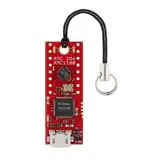
KITXMC2GOXMC1100V1TOBO1 数据手册
XMC 2Go evaluation kit user guide
About this document
Scope and purpose
This document describes the features and hardware details of the XMC 2Go equipped with the ARM® Cortex™M0 based XMC1100 microcontroller from Infineon Technologies AG.
Intended audience
This document is intended for users who use XMC 2Go kit with the XMC1100 microcontroller.
User Guide
www.infineon.com
Please read the Important Notice and Warnings at the end of this document
page 1 of 12
002-34988 Rev. **
2022-04-26
�XMC 2Go evaluation kit user guide
Table of contents
Table of contents
About this document ....................................................................................................................... 1
Table of contents ............................................................................................................................ 2
1
1.1
1.2
Overview............................................................................................................................... 3
Key features ............................................................................................................................................. 3
Block diagram.......................................................................................................................................... 3
2
2.1
2.2
2.3
2.4
Hardware description ............................................................................................................. 5
Power supply ........................................................................................................................................... 5
Pin header connector .............................................................................................................................. 6
User LEDs ................................................................................................................................................. 6
Debugging and UART communication ................................................................................................... 6
3
3.1
3.2
3.3
Production data ..................................................................................................................... 8
Schematics .............................................................................................................................................. 8
Components placement and geometry ................................................................................................. 9
List of material ......................................................................................................................................... 9
Revision history............................................................................................................................. 11
User Guide
2 of 12
002-34988 Rev. **
2022-04-26
�XMC 2Go evaluation kit user guide
Overview
1
Overview
The XMC 2Go is designed to evaluate the capabilities of the XMC1100 microcontroller and the powerful, free of
charge tool chain DAVE™.
This board is not cost optimized and does not serve as a reference design.
1.1
Key features
Table 1 summarizes the features of the XMC 2Go.
Table 1
Features of the XMC 2Go kit with XMC1100
Topic
Features
Processor
XMC1100 microcontroller (ARM® Cortex™-M0 based) in a 4 x 4 mm VQFN-24
package
Flash
32 KB or 64 KB
RAM
16 kB
Clock generation
Internal oscillator
Frequencies
32 MHz CPU clock, 64 MHz timer clock
Dimensions
14.0 x 38.5 mm
Power supply
from USB via Debug probe (J-Link) or
3.3 V external power
Connectors
Two 8-pin header (pin pitch: 2.54 mm ≙ 0.1” / between rows: 10.16 mm ≙ 0.4”)
Pin header fits to breadboard
Debugger
Onboard J-Link debugger supports
Serial wire debug (SWD, ARM standard)
Single pin debug (SPD)
UART-to-USB bridge (virtual COM)
Peripherals
Mapped to pin header X1/X2:
2 Channel USIC (UART, SPI, I2C, I2S, LIN)
6 Channel analog to digital converter (12-bit resolution)
4 x 16-bit timer
External interrupts (via ERU)
Others:
Real time clock
Random number generator
Others
2 User LEDs @ P1.0 and P1.1
1.2
Block diagram
The block diagram in Figure 1 shows the main components of the XMC 2Go kit including the power supply
concept. There are following main building blocks:
• XMC1100 microcontroller in a 4x4mm VQFN24 package
User Guide
3 of 12
002-34988 Rev. **
2022-04-26
�XMC 2Go evaluation kit user guide
Overview
• Onboard USB debugger realized with a XMC4200 microcontroller for serial wire debug (SWD) and UART-to-
USB Bridge
• Two 8-pin header X1 and X2
• Onboard power generation for power supply of the XMC1100 microcontroller and the debug IC
• 2 User LEDs
Figure 1
User Guide
Block diagram of the XMC 2Go kit
4 of 12
002-34988 Rev. **
2022-04-26
�XMC 2Go evaluation kit user guide
Hardware description
2
Hardware description
The following sections give a detailed description of the board hardware and how it can be used. Figure 2
shows the components of the XMC 2Go kit with XMC1100.
XMC4200 Debug IC and
UART to USB Bridge
Pin Header X1
User LED2
@ P1.1
Voltage Regulator &
Reverse Current Protection Diode
Pin Header distance fits
to Breadboard
Crystal for Debug IC
User LED1
@ P1.0
ESD Protection
Diode
XMC1100
Microcontroller
Power & Debug LED
Pin Header X2
Micro USB
Components.emf
Figure 2
2.1
XMC 2Go kit with XMC1100
Power supply
The XMC 2Go kit must be supplied by an external 5 Volt DC power supply connected to the Micro USB plugs
(X101). Out of the box with the preprogrammed application and the onboard debugger in operation the XMC
2Go typically draws about 75 mA. This current can be delivered via the USB plug of a PC, which is specified to
deliver up to 500 mA. The Power&Debug LED indicates the presence of the generated 3.3V supply voltage.
An onboard reverse current protection diode will ensure safe operation and protects the USB port of the
Laptop/PC in case power is provided through the pin header X1.
If the board is powered via the USB plug, it is not recommended to apply an additional power supply to the VDD
pin of X1 (3.3V), because this power supply could drive against the onboard power supply. The VDD pin can be
used to power an external circuit. But care must be taken not to draw more current than 150 mA, which is the
maximum current the onboard voltage regulator can deliver.
After power-up the Debug LED starts blinking. In case there is a connection to a PC via the Debug USB plug X101
and the USB Debug Device drivers are installed on this PC, the Debug LED will turn from blinking to constant
illumination.
User Guide
5 of 12
002-34988 Rev. **
2022-04-26
�XMC 2Go evaluation kit user guide
Hardware description
2.2
Pin header connector
The pin headers X1 and X2 can be used to extend the evaluation board or to perform measurements on the
XMC1100. The order of pins available at X1 and X2 corresponds to the pinning schema of the XMC1100
microcontroller in the TSSOP-16 pin package. The pinning table is also printed onto the bottom side of the PCB.
1
0
.5 0.0 .3V ND 2.1 2.1 2.9 2.7
0
P
P
3
G
P
P
P
P
X1
X2
P2
.6
.0
User LEDs
P2
2.3
5
.1
4
.1
.9
.8
.7
.6
Pinning of pin header
P0
P0
P0
P0
P0
P0
Figure 3
Pin_Header.emf
The port pins P1.0 and P1.2 of the XMC1100 on the XMC 2Go Kit are connected to LEDs exclusively.
Table 2
Pins used for the user LEDs
LED
Port pin
LED1
P1.1
LED2
P1.0
2.4
Debugging and UART communication
The onboard debugger supports 2-pin serial wire debug (SWD), single pin debug (SPD) and UART
communication. Both require the installation of Segger’s J-Link Driver which is part of the DAVE™ installation.
DAVE™ is a high productivity development platform for the XMC microcontroller families to simplify and
shorten SW development. It can be downloaded at www.infineon.com/dave. The latest Segger J-Link Driver
can be downloaded at https://www.segger.com/jlink-software.html.
During installation of the J-Link driver, you will be asked for the installation of optional components. For
support of the UART communication, take care to install the CDC USB driver (Composite device class).
Therefore, select the option “Install USB Driver for J-Link-OB with CDC” as shown in Figure 4.
Figure 4
User Guide
Recommended installation options for the J-Link driver
6 of 12
002-34988 Rev. **
2022-04-26
�XMC 2Go evaluation kit user guide
Hardware description
The XMC1100 on the XMC 2Go kit is configured to SWD1 mode. Use the “BMI Get Set” tool integrated into DAVE™
to configure the XMC1100 to e.g., SPD1 mode if required.
Note:
Unintended use of the “BMI Get Set” tool can cause the XMC 2Go Kit not to work anymore, e.g.,
when configuring the XMC1100 to SWD0, SPD0 mode or to productive user mode.
Note:
Do not configure the XMC1100 on the XMC 2Go kit to SWD0, SPD0 or to productive user mode.
Table 3 shows the pin assignment of the XMC1100-VQFN24 used for debugging and UART communication.
Table 3
XMC1100 pins used for debugging and UART communication
Pin function
Data pin for debugging via SWD/SPD
Input / output
Port pin
I/O
P1.3
Clock pin for debugging via SWD
O
P1.2
Transmit pin for UART communication
O
P2.1
Receive pin for UART communication
I
P2.2
User Guide
7 of 12
002-34988 Rev. **
2022-04-26
�XMC 2Go evaluation kit user guide
Production data
3
Production data
3.1
Schematics
The schematic of the XMC 2Go kit can be found in Figure 5.
Figure 5
User Guide
Schematic of the XMC 2Go kit with XMC1100
8 of 12
002-34988 Rev. **
2022-04-26
�XMC 2Go evaluation kit user guide
Production data
3.2
Components placement and geometry
Figure 6
Components placement and geometry
3.3
List of material
The list of material is valid for the XMC 2Go kit with XMC1100 version 1.
Table 4
No.
List of material
Qty
Value
Device
Reference designator
1
9
100nF 50V 0402 10% X5R CER
Capacitor
C1 C2 C101 C102 C103
C104 C105 C106 C201
2
2
15pF 50V 0402 10% COG CER
Capacitor
C109 C110
3
2
10uF 10V 0603 10% X5R CER
Capacitor
C107 C202
4
1
4.7uF 10V 0603 10% X7R CER
Capacitor
C108
5
1
NX3225SA 12MHZ AT-W
3.2X2.5
Crystal, NDK
Q101
User Guide
9 of 12
002-34988 Rev. **
2022-04-26
�XMC 2Go evaluation kit user guide
Production data
No.
Qty
Value
Device
Reference designator
6
3
100R 0402 1%
Resistor
R102 R103 R104
7
1
10k 0402 1%
Resistor
R109
8
1
1M 0402 1%
Resistor
R107
9
2
33R 0402 1%
Resistor
R105 R106
10
1
510R 0402 1%
Resistor
R108
11
3
680R 0402 1%
Resistor
R1 R2 R101
12
2
LED RT 0603 D 110mcd
LSQ976-Z
LED red
LED1 LED2
13
1
LED GN 0603 D 110mcd
LGQ971-Z
LED green
LED101
14
1
ZX62-AB-5PA
Connector, Micro-USB,
Hirose
X101
15
1
IFX54211 MBV33 SCT595
Linear Voltage Regulator,
Vout = 3.3V, Infineon
IC201
16
1
XMC1100-Q024F0032 or
XMC1100-Q024F0064
Microcontroller,
XMC1100, Cortex M0,
Infineon
IC1
17
1
XMC4200_QFN48
Microcontroller,
XMC4200, Cortex M4F,
Infineon
IC101
18
1
BAS3010A-03W SOD323-R
Diode, Infineon
D101
19
1
ESD8V0L2B-03L TSLP-3-1
TVS Diode, Infineon
D102
20
2
PINHD 8x1 0,1" TH
Pin Header, 8-pin, 0.1” TH
X1 X2
User Guide
10 of 12
002-34988 Rev. **
2022-04-26
�XMC 2Go evaluation kit user guide
Revision history
Revision history
Date
Version
Description
2022-04-26
**
Initial release
User Guide
11 of 12
002-34988 Rev. **
2022-04-26
�Trademarks
All referenced product or service names and trademarks are the property of their respective owners.
Edition 2022-04-26
Published by
Infineon Technologies AG
81726 Munich, Germany
© 2022 Infineon Technologies AG.
All Rights Reserved.
Do you have a question about this
document?
Go to www.infineon.com/support
Document reference
002-34988 Rev. **
IMPORTANT NOTICE
The information given in this document shall in no
event be regarded as a guarantee of conditions or
characteristics (“Beschaffenheitsgarantie”) .
With respect to any examples, hints or any typical
values stated herein and/or any information
regarding the application of the product, Infineon
Technologies hereby disclaims any and all
warranties and liabilities of any kind, including
without limitation warranties of non-infringement of
intellectual property rights of any third party.
In addition, any information given in this document
is subject to customer’s compliance with its
obligations stated in this document and any
applicable legal requirements, norms and standards
concerning customer’s products and any use of the
product of Infineon Technologies in customer’s
applications.
The data contained in this document is exclusively
intended for technically trained staff. It is the
responsibility of customer’s technical departments
to evaluate the suitability of the product for the
intended application and the completeness of the
product information given in this document with
respect to such application.
For further information on the product, technology,
delivery terms and conditions and prices please
contact your nearest Infineon Technologies office
(www.infineon.com).
WARNINGS
Due to technical requirements products may contain
dangerous substances. For information on the types
in question please contact your nearest Infineon
Technologies office.
Except as otherwise explicitly approved by Infineon
Technologies in a written document signed by
authorized
representatives
of
Infineon
Technologies, Infineon Technologies’ products may
not be used in any applications where a failure of the
product or any consequences of the use thereof can
reasonably be expected to result in personal injury.
�
KITXMC2GOXMC1100V1TOBO1 价格&库存
很抱歉,暂时无法提供与“KITXMC2GOXMC1100V1TOBO1”相匹配的价格&库存,您可以联系我们找货
免费人工找货- 国内价格 香港价格
- 1+96.994371+12.56417