E valu atio n B oar d
For XMC1000 Family
XMC 2 Go Kit wit h X M C11 00
Kit Version 1.0
Boa rd Us er‘s Ma nu al
Revision 1.0, 2014-02-20
Mic rocon t rolle r
�Edition 2014-02-20
Published by
Infineon Technologies AG
81726 Munich, Germany
© 2014 Infineon Technologies AG
All Rights Reserved.
Legal Disclaimer
The information given in this document shall in no event be regarded as a guarantee of conditions or
characteristics. With respect to any examples or hints given herein, any typical values stated herein and/or any
information regarding the application of the device, Infineon Technologies hereby disclaims any and all
warranties and liabilities of any kind, including without limitation, warranties of non-infringement of intellectual
property rights of any third party.
Information
For further information on technology, delivery terms and conditions and prices, please contact the nearest
Infineon Technologies Office (www.infineon.com).
Warnings
Due to technical requirements, components may contain dangerous substances. For information on the types in
question, please contact the nearest Infineon Technologies Office.
Infineon Technologies components may be used in life-support devices or systems only with the express written
approval of Infineon Technologies, if a failure of such components can reasonably be expected to cause the
failure of that life-support device or system or to affect the safety or effectiveness of that device or system. Life
support devices or systems are intended to be implanted in the human body or to support and/or maintain and
sustain and/or protect human life. If they fail, it is reasonable to assume that the health of the user or other
persons may be endangered.
�XMC 2Go
XMC 2Go Kit with XMC1100
Revision History
Page or Item
Subjects (major changes since previous revision)
Revision 1.0,
2014-02-20
Initial release
Trademarks of Infineon Technologies AG
AURIX™, C166™, CanPAK™, CIPOS™, CIPURSE™, EconoPACK™, CoolMOS™, CoolSET™,
CORECONTROL™, CROSSAVE™, DAVE™, EasyPIM™, EconoBRIDGE™, EconoDUAL™, EconoPIM™,
EiceDRIVER™, eupec™, FCOS™, HITFET™, HybridPACK™, I²RF™, ISOFACE™, IsoPACK™, MIPAQ™,
ModSTACK™, my-d™, NovalithIC™, OptiMOS™, ORIGA™, PRIMARION™, PrimePACK™, PrimeSTACK™,
PRO-SIL™, PROFET™, RASIC™, ReverSave™, SatRIC™, SIEGET™, SINDRION™, SIPMOS™,
SmartLEWIS™, SOLID FLASH™, TEMPFET™, thinQ!™, TRENCHSTOP™, TriCore™.
Other Trademarks
Advance Design System™ (ADS) of Agilent Technologies, AMBA™, ARM™, MULTI-ICE™, KEIL™,
PRIMECELL™, REALVIEW™, THUMB™, µVision™ of ARM Limited, UK. AUTOSAR™ is licensed by
AUTOSAR development partnership. Bluetooth™ of Bluetooth SIG Inc. CAT-iq™ of DECT Forum.
COLOSSUS™, FirstGPS™ of Trimble Navigation Ltd. EMV™ of EMVCo, LLC (Visa Holdings Inc.). EPCOS™
of Epcos AG. FLEXGO™ of Microsoft Corporation. FlexRay™ is licensed by FlexRay Consortium.
HYPERTERMINAL™ of Hilgraeve Incorporated. IEC™ of Commission Electrotechnique Internationale. IrDA™
of Infrared Data Association Corporation. ISO™ of INTERNATIONAL ORGANIZATION FOR
STANDARDIZATION. MATLAB™ of MathWorks, Inc. MAXIM™ of Maxim Integrated Products, Inc.
MICROTEC™, NUCLEUS™ of Mentor Graphics Corporation. Mifare™ of NXP. MIPI™ of MIPI Alliance, Inc.
MIPS™ of MIPS Technologies, Inc., USA. muRata™ of MURATA MANUFACTURING CO., MICROWAVE
OFFICE™ (MWO) of Applied Wave Research Inc., OmniVision™ of OmniVision Technologies, Inc.
Openwave™ Openwave Systems Inc. RED HAT™ Red Hat, Inc. RFMD™ RF Micro Devices, Inc. SIRIUS™ of
Sirius Satellite Radio Inc. SOLARIS™ of Sun Microsystems, Inc. SPANSION™ of Spansion LLC Ltd.
Symbian™ of Symbian Software Limited. TAIYO YUDEN™ of Taiyo Yuden Co. TEAKLITE™ of CEVA, Inc.
TEKTRONIX™ of Tektronix Inc. TOKO™ of TOKO KABUSHIKI KAISHA TA. UNIX™ of X/Open Company
Limited. VERILOG™, PALLADIUM™ of Cadence Design Systems, Inc. VLYNQ™ of Texas Instruments
Incorporated. VXWORKS™, WIND RIVER™ of WIND RIVER SYSTEMS, INC. ZETEX™ of Diodes Zetex
Limited.
Last Trademarks Update 2011-02-24
Template: IFX_Template_2011-02-24.dot
�XMC 2Go
XMC 2Go Kit with XMC1100
Table of Contents
Table of Contents
Introduction ............................................................................................................................................................ 7
1
1.1
1.2
Overview ............................................................................................................................................. 7
Key Features ........................................................................................................................................ 7
Block Diagram ...................................................................................................................................... 8
2
2.1
2.2
2.3
2.4
Hardware Description ........................................................................................................................ 9
Power Supply ....................................................................................................................................... 9
Pin Header Connector ........................................................................................................................ 10
User LEDs .......................................................................................................................................... 10
Debugging and UART Communication .............................................................................................. 11
3
3.1
3.2
3.3
Production Data................................................................................................................................ 11
Schematics ......................................................................................................................................... 11
Components Placement and Geometry ............................................................................................. 13
List of Material .................................................................................................................................... 14
Board Users Manual
4
Revision 1.0, 2014-02-20
�XMC 2Go
XMC 2Go Kit with XMC1100
List of Figures
List of Figures
Figure 1
Figure 2
Figure 3
Figure 4
Figure 5
Figure 6
Block Diagram of the XMC 2Go Kit ...................................................................................................... 8
XMC 2Go Kit with XMC1100 ................................................................................................................ 9
Pinning of Pin Header ........................................................................................................................ 10
Recommended Installation Options for the J-Link driver ................................................................... 11
Schematic of the XMC 2Go Kit with XMC1100 .................................................................................. 12
Components Placement and Geometry ............................................................................................. 13
Board Users Manual
5
Revision 1.0, 2014-02-20
�XMC 2Go
XMC 2Go Kit with XMC1100
List of Tables
List of Tables
Table 1
Table 2
Table 3
Table 4
Features of the XMC 2Go Kit with XMC1100 ...................................................................................... 7
Pins used for the User LEDs .............................................................................................................. 10
XMC1100 Pins used for Debugging and UART Communication ....................................................... 11
List of Material .................................................................................................................................... 14
Board Users Manual
6
Revision 1.0, 2014-02-20
�XMC 2Go
XMC 2Go Kit with XMC1100
Overview
Introduction
This document describes the features and hardware details of the XMC 2Go equipped with the ARM® Cortex™M0 based XMC1100 Microcontroller from Infineon Technologies AG.
1
Overview
The XMC 2Go is designed to evaluate the capabilities of the XMC1100 Microcontroller and the powerful, free of
charge tool chain DAVE™.
This board is not cost optimized and does not serve as a reference design.
1.1
Key Features
Table 1 summarizes the features of the XMC 2Go.
Table 1
Features of the XMC 2Go Kit with XMC1100
Topic
Features
Flash
XMC1100 microcontroller (ARM® Cortex™-M0 based) in a 4 x 4 mm VQFN-24
package
64 kB
RAM
16 kB
Clock Generation
Internal Oscillator
Frequencies
32 MHz CPU clock, 64 MHz Timer clock
Dimensions
14.0 x 38.5 mm
Processor
Power Supply
from USB via Debug probe (J-Link) or
3.3V external power
Connectors
Two 8-pin header (pin pitch: 2.54 mm ≙ 0.1” / between rows: 10.16 mm ≙ 0.4”)
Pin header fits to breadboard
Debugger
On-Board J-Link Debugger supports
Serial Wire Debug (SWD, ARM Standard)
Single Pin Debug (SPD)
UART-to-USB bridge (virtual COM)
Mapped to pin header X1/X2:
2 Channel USIC (UART, SPI, I2C, I2S, LIN)
6 Channel Analog to Digital Converter (12-Bit resolution)
4 x 16-Bit Timer
External Interrupts (via ERU)
Others:
Real Time Clock
Random Number Generator
Peripherals
Others
Board Users Manual
2 User LEDs @ P1.0 and P1.1
7
Revision 1.0, 2014-02-20
�XMC 2Go
XMC 2Go Kit with XMC1100
Overview
1.2
Block Diagram
The block diagram in Figure 1 shows the main components of the XMC 2Go Kit including the power supply
concept. There are following main building blocks:
XMC1100 Microcontroller in a 4x4mm VQFN24 package
On-board USB debugger realized with a XMC4200 Microcontroller for serial wire debug (SWD) and
UART-to-USB Bridge
Two 8 pin header X1 and X2
On-board power generation for power supply of the XMC1100 Microcontroller and the debug IC
2 User LEDs
8-Pin Header X1
P2.7/P2.8, P2.9, P2.10, P2.11, P0.0, P0.5
X1
+5V
Voltage
Regulator
ADC, CCU4, USIC, ERU0
LED2
LED1
P1.1
P1.0
GPIO
+3.3V
EVR
XMC1100 VQFN24
USIC
32MHz Cortex M0
64kB Flash, 16kB RAM
4 x16-bit timer, 6 Ch 12-bit ADC
Debug,
BSL
USIC
2 Ch USIC (UART, SPI, I2C, I2S, LIN)
P2.1
P2.2
UART
P1.2
P1.3
SWD
+3.3V
XMC4200
Debug IC
Micro
USB
X101
Debug
LED
ADC, CCU4, USIC, ERU0
XMC 2Go-V1 Kit
XMC1100 in VQFN24
X2
8-Pin Header X2
P0.6-P0.9, P0.14, P0.15, P2.0, P2.6
Block_Diag.emf
Figure 1
Block Diagram of the XMC 2Go Kit
Board Users Manual
8
Revision 1.0, 2014-02-20
�XMC 2Go
XMC 2Go Kit with XMC1100
Hardware Description
2
Hardware Description
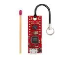
The following sections give a detailed description of the board hardware and how it can be used. Figure 2
shows the components of the XMC 2Go Kit with XMC1100.
XMC4200 Debug IC and
UART to USB Bridge
Pin Header X1
User LED2
@ P1.1
Voltage Regulator &
Reverse Current Protection Diode
Pin Header distance fits
to Breadboard
Crystal for Debug IC
User LED1
@ P1.0
ESD Protection
Diode
XMC1100
Microcontroller
Power & Debug LED
Pin Header X2
Micro USB
Components.emf
Figure 2
2.1
XMC 2Go Kit with XMC1100
Power Supply
The XMC 2Go Kit must be supplied by an external 5 Volt DC power supply connected to the Micro UBS plugs
(X101). Out of the box with the pre-programmed application and the on-board debugger in operation the XMC
2Go typically draws about 75 mA. This current can be delivered via the USB plug of a PC, which is specified to
deliver up to 500 mA. The Power&Debug LED indicates the presence of the generated 3.3V supply voltage.
An on-board reverse current protection diode will ensure safe operation and protects the USB port of the
Laptop/PC in case power is provided through the pin header X1.
If the board is powered via the USB plug, it’s not recommended to apply an additional power supply to the VDD
pin of X1 (3.3V), because this power supply could drive against the on-board power supply. The VDD pin can be
used to power an external circuit. But care must be taken not to draw more current than 150 mA, which is the
maximum current the on-board voltage regulator can deliver.
After power-up the Debug LED starts blinking. In case there is a connection to a PC via the Debug USB plug
X101 and the USB Debug Device drivers are installed on this PC, the Debug LED will turn from blinking to
constant illumination.
Board Users Manual
9
Revision 1.0, 2014-02-20
�XMC 2Go
XMC 2Go Kit with XMC1100
Hardware Description
2.2
Pin Header Connector
P2
P2
P2
P2
X2
X1
.7
P2
P0
.9
P2
P0
.1
0
G
N
P0
.1
1
3.
3V
P0
.0
P0
P0
.5
P0
P0
D
The pin headers X1 and X2 can be used to extend the evaluation board or to perform measurements on the
XMC1100. The order of pins available at X1 and X2 corresponds to the pinning schema of the XMC1100
Microcontroller in the TSSOP-16 pin package. The pinning table is also printed onto the bottom side of the PCB.
.6
.0
5
.1
4
.1
.9
.8
2.3
.7
.6
Figure 3
Pin_Header.emf
Pinning of Pin Header
User LEDs
The port pins P1.0 and P1.2 of the XMC1100 on the XMC 2Go Kit are connected to LEDs exclusively.
Table 2
Pins used for the User LEDs
LED
Port Pin
LED1
P1.1
LED2
P1.0
Board Users Manual
10
Revision 1.0, 2014-02-20
�XMC 2Go
XMC 2Go Kit with XMC1100
Production Data
2.4
Debugging and UART Communication
The on-board debugger supports 2-pin Serial Wire Debug (SWD), Single Pin Debug (SPD) and UART
communication. Both require the installation of Segger’s J-Link Driver which is part of the DAVE™ installation.
DAVE™ is a high-productivity development platform for the XMC microcontroller families to simplify and shorten
SW development. It can be downloaded at www.infineon.com/dave. The latest Segger J-Link Driver can be
downloaded at http://www.segger.com/jlink-software.html.
During installation of the J-Link driver you will be asked for the installation of optional components. For support
of the UART communication take care to install the CDC USB driver (Composite Device Class). Therefore
select the option “Install USB Driver for J-Link-OB with CDC” as shown in Figure 4.
Figure 4
Recommended Installation Options for the J-Link driver
The XMC1100 on the XMC 2Go Kit is configured to SWD1 mode. Use the “BMI Get Set” tool integrated into
DAVE™ to configure the XMC1100 to e.g. SPD1 mode if required. Take care: Unintended use of the “BMI Get
Set” tool can cause the XMC 2Go Kit not to work anymore, e.g. when configuring the XMC1100 to SWD0, SPD0
mode or to productive user mode.
Note: Do not configure the XMC1100 on the XMC 2Go Kit to SWD0, SPD0 or to productive user mode.
Table 3 shows the pin assignment of the XMC1100-VQFN24 used for debugging and UART communication.
Table 3
XMC1100 Pins used for Debugging and UART Communication
Pin Function
Input / Output
Port Pin
Data pin for Debugging via SWD/SPD
I/O
P1.3
Clock pin for Debugging via SWD
O
P1.2
Transmit Pin for UART Communication
O
P2.1
Receive Pin for UART Communication
I
P2.2
3
Production Data
3.1
Schematics
The schematic of the XMC 2Go Kit can be found in Figure 5.
Board Users Manual
11
Revision 1.0, 2014-02-20
�E
D
C
B
Target Device (XMC1100)
+5V
GND
1
4
1
EN
IN
IC201
Power Supply
GND
C1
GND
OUT
3
IFX54211 MBV33
C2
100nF/0402 100nF/0402
+3V3
1
2
3
4
5
6
7
8
X1
PINHD 8x1 0,1" TH
P2.7/P2.8
P2.9
P2.10
P2.11
GND
+3V3
P0.0
P0.5
P2.6
P2.0
P0.15
P0.14
P0.9
P0.8
P0.7
P0.6
+3V3
2
GND
LEDs
P1.0/LED1
P1.1/LED2
P2.7/P2.8
P2.9
P2.10
P2.11
RX_XMC4200
TX_XMC4200P2.6
P1.0/LED1
P1.1/LED2
P1.2/SWCLK
P1.3/SWDP2.0
P0.0
P0.5
P0.6
P0.7
P0.8
P0.9
P0.12
P0.13
P0.14
P0.15
PINHD 8x1 0,1" TH
16
15
14
13
12
11
10
9
X2
TSSOP-16 Pinout
10
9
EXP
15
16
17
18
19
20
21
22
23
24
14
13
12
11
1
2
3
4
5
6
7
8
Supply
LED RT/0603
LED1
3
LED RT/0603
LED2
XMC1100_VQFN24
VDD
VSS
EXP
P0.0
P0.5
P0.6
P0.7
P0.8
P0.9
P0.12
P0.13
P0.14
P0.15
P1.0
P1.1
P1.2
P1.3
P2.0
P2.1
P2.2
P2.6
P2.8
P2.9
P2.10
P2.11
IC1
GND
GND
Q101
+3V3
29
30
GND
Analog
Digital
VDDC1
VDDC
VDDP2
VDDP1
VDDP
31
6
41
28
5
3
4
7
10
19
20
11
12
13
14
15
16
35
36
37
38
39
40
42
43
44
45
46
47
48
1
2
5
6
The information given in this document shall in no event be regarded as a guarantee of conditions or
characteristics. With respect to any examples or hints given herein, any typical values stated herein and/or any
information regarding the application of the device, Infineon Technologies hereby disclaims any and all warranties
and liabilities of any kind, including without limitation, warranties of non-infringement of intellectual property rights
of any third party.
Legal Disclaimer
8
R105
R106
7
GND
+3V3
GND
+5V
X101S
100nF/0402
C101
Sheet: 1/1
8
13.02.2014 15:43:12
XMC 2Go-V1 Kit
XMC_2Go-V1
Target Device : 1-99
Debugging Device : 100-199
Power Supply : 200-299
GNDGNDGND GND
1
2
3
4
5
X101C
P1.2/SWCLK
100R/0402
TX_XMC4200
RX_XMC4200
P1.3/SWD
33R/0402
33R/0402
GND
R104
COM LED
Level Shifter
No RESET Pin
UART
SPD
SWV
JTAG
SWCLK
R103
+3V3
680R/0402
R101
100R/0402
100R/0402
DEBUG_LED#
R102
For further information and software examples please visit www.infineon.com/xmc-dev
Supply
USB_D-
HIB_IO_0
VBAT
P14.9
P14.8
P14.7
P14.6
P14.5
P14.4
P14.3
P14.0
P1.5
P1.4
P1.3
P1.2
P1.1
P1.0
P0.8
P0.7
P0.6
P0.5
P0.4
P0.3
P0.2
P0.1
P0.0
USB USB_D+
Hibernate/RTC
XMC4200_QFN48
VSS
PORST#
TCK
TMS
XTAL1
XTAL2
RTC_XTAL_1
RTC_XTAL_2
VAREF
VAGND
P2.5
P2.4
P2.3
P2.2
P2.1
P2.0
IC101
PINHD 1x5 0,05" TH
1
2
3
4
5
SV1
27
510R/0402
+3V3
GND
R108
8
9
18
17
DBG_RESET
DBG_TCK
DBG_TMS
U1C0
DX0A-P0.4
DOUT0-P0.5
GPIO-P0.7
GPIO-P0.6
UART2 (DM2)
RXD
TXD
TX_ENABLE
TXACTIVE#
21
22
23
24
25
26
32
34
33
P14.9
ADC
AIN
RESET#
GPIO-P0.3
DEBUG_LED# GPIO-P0.2
AUX_LED#
GPIO-P0.1
U0C1
DX2A-P2.3
DX1A-P2.4
GPIO-P0.8
SPI Slave
CS_IN
CLK_IN
PULL Select
GND
4
DEBUG_LED#
RXD
TXD
SWD_IN
SWD_OUT
SWCLK
SWCLK
C106 100nF/0402
U0C0
GPIO-P1.3
DX0B-P1.4
DOUT0-P1.5
SCLKOUT-P1.1
SELO0-P1.0
C108 4,7uF/0603
SPI Master
SWD DIR
MISO
MOSI
CLK_OUT
CS_OUT
C105 100nF/0402
Debug Connection Concept
C104 100nF/0402
XMC1100 in VQFN24
C110 15pF/0402
Configure wiggler-P0.5 as USIC_Tx but only active while X-spy function is selected
Configure wiggler-P0.4 as USIC_Rx but only active while X-spy function is selected
C103 100nF/0402
XMC 2Go Kit
C109 15pF/0402
7
D102
6
3 D1
5
LED101
LED GN/0603
4
C102 100nF/0402
On-board Debugger including a UART to USB Bridge
C107 10uF/0603
PinHeader XMC1100
C201 100nF/0402
P2 P1
C202 10uF/0603
3
680R/0402
ESD8V0L2B-03L 1
2
680R/0402
R1
A
C
D101
2
D2
A
GND1
GND2
2
5
R109
12
R2
BAS3010A-03W
R107
Board Users Manual
10k/0402
ZX62-AB-5PA
Figure 5
1M/0402
1
E
D
C
B
A
XMC 2Go
XMC 2Go Kit with XMC1100
Production Data
Schematic of the XMC 2Go Kit with XMC1100
Revision 1.0, 2014-02-20
�XMC 2Go
XMC 2Go Kit with XMC1100
Production Data
3.2
Components Placement and Geometry
X101
IC201
D101
C202
C201
C104 D102 R107
C106
R109
C103
R106 R105 C101
R101
IC101
38.5 mm
C107
LED101
R102
C102 C109R108
Q101
C105
C108
C110 R104
R103
C2 C1
IC1
P2
P1
LED2
R2
LED1
R1
14.0 mm
Figure 6
Components Placement and Geometry
Board Users Manual
13
Revision 1.0, 2014-02-20
�XMC 2Go
XMC 2Go Kit with XMC1100
Production Data
3.3
List of Material
The list of material is valid for the XMC 2Go Kit with XMC1100 Version 1.
Table 4
No.
List of Material
Qty Value
14
9
2
2
1
1
3
1
1
2
1
3
2
1
1
15
1
16
1
17
1
1
1
2
1
2
3
4
5
6
7
8
9
10
11
12
13
18
19
20
100nF 50V 0402 10% X5R CER
15pF 50V 0402 10% COG CER
10uF 10V 0603 10% X5R CER
4.7uF 10V 0603 10% X7R CER
NX3225SA 12MHZ AT-W 3.2X2.5
100R 0402 1%
10k 0402 1%
1M 0402 1%
33R 0402 1%
510R 0402 1%
680R 0402 1%
LED RT 0603 D 110mcd LSQ976-Z
LED GN 0603 D 110mcd LGQ971-Z
ZX62-AB-5PA
IFX54211 MBV33 SCT595
XMC1100_VQFN24
XMC4200_QFN48
BAS3010A-03W SOD323-R
ESD8V0L2B-03L TSLP-3-1
PINHD 8x1 0,1" TH
Board Users Manual
Device
Capacitor
Capacitor
Capacitor
Capacitor
Crystal, NDK
Resistor
Resistor
Resistor
Resistor
Resistor
Resistor
LED red
LED green
Connector, Micro-USB, Hirose
Linear Voltage Regulator, Vout =
3.3V, Infineon
Microcontroller, XMC1100, Cortex
M0, Infineon
Microcontroller, XMC4200, Cortex
M4F, Infineon
Diode, Infineon
TVS Diode, Infineon
Pin Header, 8-pin, 0.1” TH
14
Reference Designator
C1 C2 C101 C102 C103
C104 C105 C106 C201
C109 C110
C107 C202
C108
Q101
R102 R103 R104
R109
R107
R105 R106
R108
R1 R2 R101
LED1 LED2
LED101
X101
IC201
IC1
IC101
D101
D102
X1 X2
Revision 1.0, 2014-02-20
�w w w . i n f i n e o n . c o m
Published by Infineon Technologies AG
�


 工商网监
湘ICP备2023018690号
工商网监
湘ICP备2023018690号

