PTFB191501EV1R250XTMA1 数据手册
PTFB191501E
PTFB191501F
Confidential, Limited Internal Distribution
Thermally-Enhanced High Power RF LDMOS FETs
150 W, 1930 – 1990 MHz
Description
-20
40
Efficiency
15
IMD Low
sc
on
-55
31
33
35
37
39
41
43
45
5
0
47
s
•
Typical CW performance, 1990 MHz, 30 V
- Output power at P–1dB = 150 W
- Efficiency = 55%
•
Increased negative gate-source voltage range for
improved performance in Doherty peaking
amplifiers
•
Integrated ESD protection: Human Body Model,
Class 2 (minimum)
•
Excellent thermal stability, low HCI drift
•
Capable of handling 10:1 VSWR @ 30 V, 150 W
(CW) output power
•
Pb-free, RoHS-compliant
10
ACPR
-60
Typical two-carrier WCDMA performance at
1990 MHz, 30 V
- Average output power = 35 W
- Linear gain = 18 dB
- Efficiency = 30%
- Intermodulation distortion = –35 dBc
d
ue
20
Efficiency (%)
25
-50
Broadband internal matching
•
35
tin
IMD (dBc)
-35
-45
•
30
IMD Up
-40
pr
od
VDD = 30 V, IDQ = 1.20 A, ƒ = 1990 MHz, 3GPP WCDMA,
PAR = 8 dB, 10 MHz carrier spacing, BW 3.84 MHz
-30
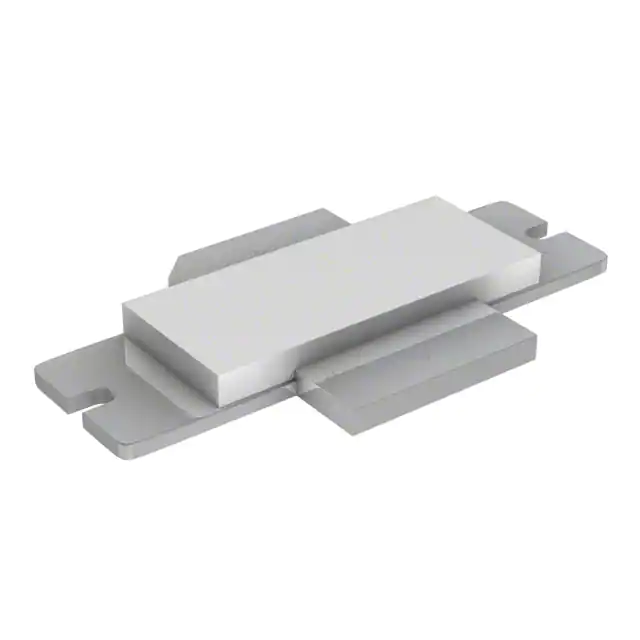
PTFB191501F
Package H-37248-2
Features
Two-carrier WCDMA Drive-up
-25
PTFB191501E
Package H-36248-2
uc
t
The PTFB191501E and PTFB191501F are 150-watt LDMOS FETs
designed for single- and two-carrier WCDMA and CDMA applications
from 1930 to 1990 MHz. Features include input and output matching,
and thermally-enhanced, RoHs-compliant package with slotted and
earless flanges. Manufactured with Infineon's advanced LDMOS
process, these devices provide excellent thermal performance and
superior reliability.
49
di
Output Power (dBm)
RF Characteristics
Two-carrier WCDMA Measurements (not subject to production test—verified by design/characterization in Infineon test fixture)
VDD = 30 V, IDQ = 1.2 A, POUT = 35 W average, ƒ1 = 1985 MHz, ƒ2 = 1995 MHz, 3GPP signal, channel bandwidth = 3.84 MHz,
peak/average = 8 dB @ 0.01% CCDF
Characteristic
Symbol
Min
Typ
Max
Unit
Gain
Gps
—
18
—
dB
Drain Efficiency
ηD
—
30
—
%
Intermodulation Distortion
IMD
—
–35
—
dBc
All published data at TCASE = 25°C unless otherwise indicated
*See Infineon distributor for future availability.
ESD: Electrostatic discharge sensitive device—observe handling precautions!
Data Sheet
1 of 15
Rev. 03, 2015-01-14
�PTFB191501E
PTFB191501F
Confidential, Limited Internal Distribution
RF Characteristics (cont.)
Two-tone Measurements (tested in Infineon test fixture)
VDD = 30 V, IDQ = 1.2 A, POUT = 150 W PEP, ƒ = 1990 MHz, tone spacing = 1 MHz
Min
Typ
Max
Unit
Gain
Gps
17
18
—
dB
Drain Efficiency
ηD
42
44
—
%
Intermodulation Distortion
IMD
—
–28
dBc
Min
Typ
Max
Unit
Drain-Source Breakdown Voltage
VGS = 0 V, IDS = 10 mA
V(BR)DSS
65
—
—
V
Drain Leakage Current
VDS = 28 V, V GS = 0 V
IDSS
—
—
1.0
µA
Drain Leakage Current
VDS = 63 V, V GS = 0 V
IDSS
—
—
10.0
µA
On-State Resistance
VGS = 10 V, V DS = 0.1 V
RDS(on)
—
0.08
—
Ω
Operating Gate Voltage
VDS = 28 V, IDQ = 1.2 A
VGS
2.4
2.9
3.4
V
Gate Leakage Current
VGS = 10 V, V DS = 0 V
IGSS
—
—
1.0
µA
Maximum Ratings
ue
Symbol
Value
Unit
Drain-Source Voltage
VDSS
65
V
Gate-Source Voltage
VGS
–6 to +10
V
Junction Temperature
TJ
200
°C
Storage Temperature Range
TSTG
–40 to +150
°C
Thermal Resistance (TCASE = 70°C, 200 W CW)
RθJC
0.29
°C/W
di
sc
on
Parameter
Symbol
pr
od
Conditions
d
Characteristic
–30
tin
DC Characteristics
s
Symbol
uc
t
Characteristic
Ordering Information
Type and Version
Package Type
Package Description
Shipping
PTFB191501E V1
H-36248-2
Thermally-enhanced slotted flange, single-ended
Tray
PTFB191501E V1 R250
H-36248-2
Thermally-enhanced slotted flange, single-ended
Tape & Reel 250 pcs
PTFB191501F V1
H-37248-2
Thermally-enhanced earless flange, single-ended
Tray
PTFB191501F V1 R250
H-37248-2
Thermally-enhanced earless flange, single-ended
Tape & Reel 250 pcs
*See Infineon distributor for future availability.
Data Sheet
2 of 15
Rev. 03, 2015-01-14
�PTFB191501E
PTFB191501F
Confidential, Limited Internal Distribution
Typical Performance (data taken in a production test fixture)
Two-carrier WCDMA 3GPP Drive-up
Two-carrier WCDMA 3GPP
VDD = 30 V, IDQ = 1.20 A, 3GPP WCDMA,
PAR = 8 dB, 10 MHz carrier spacing, BW 3.84 MHz
VDD = 30 V, IDQ = 1.20 A, ƒ = 1990 MHz, 3GPP WCDMA,
PAR = 8 dB, 10 MHz carrier spacing, BW 3.84 MHz
-40
s
19
Gain
18
17
pr
od
-45
-50
40
uc
t
-35
Gain (dB)
Drain Efficiency (%)
-30
50
20
1990 MHz Low
1990 MHz Up
1960 MHz Low
1960 MHz Up
1930 MHz Low
1930 MHz Up
30
20
Efficiency
10
16
-55
0
15
-60
31
33
35
37
39
41
43
45
47
31
49
33
35
37
Drain Efficiency (%)
-25
39
41
43
45
47
49
Output Power (dBm)
tin
ue
d
Output Power (dBm)
CW Power Sweep
Gain & Efficiency vs. Output Power
Two-tone Broadband Performance
VDD = 30 V, IDQ = 1.20 A, POUT = 63 W
45
di
Gain (dB)
55
Gain
18
17
16
Gain / Efficiency (dB / %)
19
60
65
35
25
Efficiency
15
Drain Efficiency (%)
20
15
14
43
45
47
49
51
50
45
-15
Efficiency
40
35
-10
-20
-25
IMD3
30
-30
-35
25
-40
Gain
-45
15
-50
1890 1910 1930 1950 1970 1990 2010 2030
53
Output Power (dBm)
Data Sheet
-5
IRL
20
5
41
55
Return Loss (dB), IMD (dBc)
sc
on
VDD = 30 V, IDQ = 1.20 A, ƒ = 1990 MHz
Frequency (MHz)
3 of 15
Rev. 03, 2015-01-14
�PTFB191501E
PTFB191501F
Confidential, Limited Internal Distribution
Typical Performance (cont.)
Two-tone Drive-up
Two-tone Drive-up
VDD = 30 V, IDQ = 1.20 A,
VDD = 30 V, IDQ = 1.20 A,
ƒ1 = 1990 MHz, ƒ2 = 1989 MHz
ƒ 1 = 1990 MHz, ƒ2 = 1989 MHz
-35
35
-40
30
IMD3
-45
25
-50
20
-55
15
-60
10
5
-65
40
42
44
46
48
50
52
54
Output Power, PEP (dBm )
55
Gain
19
18
45
35
Efficiency
17
pr
od
40
Gain (dB)
IMD (dBc)
45
Efficiency
-30
Efficiency (%)
-25
20
25
16
15
15
40
42
44
Efficiency (%)
50
s
55
-20
uc
t
-15
5
46
48
50
52
54
tin
ue
d
Output Power, PEP (dBm)
Intermodulation Distortion vs. Output Power
VDD = 30 V, IDQ = 1.20 A, Tone Spacing = 1 MHz
VDD = 30 V, IDQ = 1.20 A, ƒ 1 = 1990 MHz, ƒ2 = 1989 MHz
sc
on
Two-tone Drive-up at Selected Frequencies
-20
-20
3rd
1990 MHz
-30
-30
IMD (dBc)
1930 MHz
-40
di
IMD (dBc)
1960 MHz
-50
-60
5th
-40
7th
-50
-60
-70
41
43
45
47
49
51
-70
53
40
Output Power, PEP (dBm)
Data Sheet
45
50
55
Output Power, PEP (dBm)
4 of 15
Rev. 03, 2015-01-14
�PTFB191501E
PTFB191501F
Confidential, Limited Internal Distribution
Typical Performance (cont.)
CW Performance
Gain & Efficiency vs. Output Power
CW Performance
Gain vs. Output Power
VDD = 30 V, IDQ = 1.20 A, ƒ = 1990 MHz
VDD = 30 V, ƒ = 1990 MHz
19
21
18
30
17
20
Gain
10
16
s
uc
t
40
18
IDQ = 1.20 A
IDQ = 0.80 A
17
pr
od
19
Power Gain (dB)
50
Drain Efficiency (%)
20
Gain (dB)
Efficiency
–10 °C
25 °C
85 °C
IDQ = 1.40 A
60
16
43 44 45 46 47 48 49 50 51 52 53
42
Output Power (dBm)
44
46
48
50
52
54
tin
ue
d
Output Power (dBm)
Gate-Source Voltage vs. Case Temperature
Voltage normalized to typical gate voltage.
Series show current.
sc
on
Single-carrier WCDMA
VDD = 30 V, IDQ = 1.20A, f = 1990 MHz
3GPP_WCDMA, PAR = 8dB, BW 3.84MHz
-20
40
1.03
-40
20
-50
10
ACP up
ACP low
-60
Drain Efficiency (%)
30
di
ACP (dBc)
-30
Normalized Bias Voltage
Efficiency
0
31
33
35
37
39
41
43
45
47
1.01
1.00
0.40 A
1.53 A
2.67 A
3.80 A
4.93 A
6.07 A
0.99
0.98
0.97
0.96
0.95
49
-20
Output Power (dBm)
Data Sheet
1.02
0
20
40
60
80
100
Case Temperature (°C)
5 of 15
Rev. 03, 2015-01-14
��PTFB191501E
PTFB191501F
Confidential, Limited Internal Distribution
Reference Circuit
8
1
In
C802
100000 pF
C106
10000000 pF
TL115
4
3
NC
3
6
TL121
TL117
TL119
s
1
2
1
1
3
1
R102
5100 Ohm
2
2
3
3
C102
1000000 pF
2
TL122
C103
20000 pF
TL123
Er=4.5
H=30 mil
TMM/TMM4
TL104
X PORT
RF_IN
3
2
TL109
TL111
C101
10 pF
R103
10 Ohm
TL126
TL125
TL120
TL124
TL110
TL127
TL128
pr
od
3
1
TL107
TL108
TL112
1
R801
1000 Ohm
C803
100000 pF
S1
4
S
3 E
C105
10 pF
TL118
TL129
B
3
S3
uc
t
R101
2000 Ohm
5
2 C
1
R804
1300 Ohm
C104
20000 pF
7
C801
100000 pF
R803
1200 Ohm
2
Out
NC
2
1
TL116
R802
1000 Ohm
S2
VGS1
TL113
TL106
TL130
C107
0.7 pF
TL102
TL103
TL114
TL101
TL105
3
2
3
1
2
1
1 5
0
1
e
f -
v 1
_ B
D
_
i n
_
0
8 -
3
0 -
0
9
GATE
DUT
PORT
2 Pin 1
ue
d
b1 9
TL242
TL237
TL234
1
2
3
TL245
TL220
TL240
sc
on
TL241
tin
Reference circuit input schematic for ƒ = 1990 MHz
TL223
TL230
TL227
1
TL229
TL224
2
1
3
2
1
TL226
2
3
3
VDD1
C210
20000 pF
C208
1000000 pF
C212
10000000 pF
C206
10 pF
TL210
C201
0.7 pF
TL213
TL208
TL201
TL211
2
di
DRAIN
PORT
DUT
Pin
1D
TL203
TL219
3
1
2
TL204
TL205
TL215
TL202
3
1
1
TL206
TL216
C204
10 pF
TL207
TL217
TL218
TL246
2
1
3
4
2
3
4
TL212
C202
0.7 pF
TL214
TL247
C203
0.6 pF
C213
0.6 pF
TL248
PORT
RF_OUT
2
X
TL209
C205
10 pF
C209
20000 pF
TL243
TL235
TL236
TL244
TL238
TL221
3
2
TL239
TL222
TL231
1
C207
10000000 pF
C211
1000000 pF
TL232
TL228
3
2
1
TL225
3
2
1
9
1
5
0
1
e
f - v
1
_ B
D
_
o
u
t _
0
8 - 3
0
- 0
TL233
3
2
b 1
1
9
VDD2
Reference circuit output schematic for ƒ = 1990 MHz
Data Sheet
7 of 15
Rev. 03, 2015-01-14
�PTFB191501E
PTFB191501F
Confidential, Limited Internal Distribution
Reference Circuit (cont.)
VDD
R802 C801 C802
S3
C105
R102
C102 C103
RF_IN
C206
S2
s
R801
C803
VDD
uc
t
R101
R804
R803
S1
C210
C208
C201
R103 C107
C212
C204
pr
od
C106 C104
C101
C202
RF_OUT
C213
C203
C207
C211
C209
VDD
sc
on
tin
ue
d
C205
b 1 9 1 5 0 1 e f - v 1 _ C D _ 9 - 2 -0 9
Reference circuit assembly diagram (not to scale)*
di
Circuit Assembly Information
DUT
PTFB191501E or PTFB191501F
INPUT PCB
0.762 mm [.030"] thick, εr = 4.5
OUTPUT PCB
0.762 mm [.030"] thick, εr = 4.5
LDMOS Transistor
TMM 4
TMM 4
2 oz. copper
2 oz. copper
*Gerber files for this circuit available on request
Data Sheet
8 of 15
Rev. 03, 2015-01-14
�PTFB191501E
PTFB191501F
Confidential, Limited Internal Distribution
Reference Circuit (cont.)
Components List
Suggested
Manufacturer
Part Number
Chip capacitor
Chip capacitor
Chip capacitor
Chip capacitor
Capacitor, 10 µF, 35 V
Chip capacitor
Chip capacitor
10 pF
1000000 pF
20000 pF
10 pF
10000000 pF
0.7 pF
100000 pF
ATC
ATC
ATC
ATC
Digi-Key
ATC
ATC
ATC100B100FW500XB
445-1411-2-ND
ATC100B102FW50XB
ATC100B100FW500XB
399-1655-2-ND
Tantalum
ATC100B0R7BW500XB
PCC104BCT-ND
Resistor
Resistor
Resistor
Resistor
Resistor
Resistor
Transistor
Voltage regulator
2000 ohm
5100 ohm
10 ohm
1000 ohm
1200 ohm
1300 ohm
S3
Potentiometer
2k ohms
Digi-Key
Digi-Key
Digi-Key
Digi-Key
Digi-Key
Digi-Key
Infineon
National
Semiconductor
Digi-Key
Output
C201
C202
C203
C204
C205
C206
C207
C208
C209
C210
C211
C212
C213
Chip capacitor
Chip capacitor
Chip capacitor
Chip capacitor
Chip capacitor
Chip capacitor
Capacitor, 10 µF, 35 V
Chip capacitor
Chip capacitor
Chip capacitor
Chip capacitor
Capacitor, 10 µF, 35 V
Chip capacitor
Data Sheet
tin
0.7 pF
0.7 pF
0.6 pF
10 pF
10 pF
10 pF
10000000 pF
1000000 pF
20000 pF
20000 pF
1000000 pF
10000000 pF
0.6 pF
sc
on
di
uc
t
pr
od
d
Input
C101
C102
C103, C104
C105
C106
C107
C801, C802,
C803
R101
R102
R103
R801, R802
R803
R804
S1
S2
Comment
s
Value
ue
Schematic ID Component
Type
P2.0KECT-ND
P5.1KECT-ND
P100ECT
P1.0KECT-ND
P1.2KGECT-ND
P1.3KGECT-ND
BCP56
LM7805
3224W-202ECT-ND
ATC
100B0R7BW500XB
ATC
100B0R7BW500XB
ATC
100B0R6BW500XB
ATC
100B100FW500XB
ATC
100B100FW500XB
ATC
100B100FW500XB
Garrett Electronics TPSE106K050R0400
ATC
445-1411-2-ND
ATC
100B102FW50XB
ATC
100B102FW50XB
ATC
445-1411-2-ND
Garrett Electronics TPSE106K050R0400
ATC
100B0R6BW500XB
9 of 15
Tantalum
Tantalum
Rev. 03, 2015-01-14
�PTFB191501E
PTFB191501F
Confidential, Limited Internal Distribution
Reference Circuit (cont.)
Electrical Characteristics at 1990 MHz
Electrical
1st/4th Dimension
2nd Dimension
W2
6.87 Ω
0.241 λ
W1 17.780 mm
132.58 Ω
0.000 λ
W
MLIN
TL103
MSTEP
TL104
MLIN
50.98 Ω
0.312 λ
W
1.397 mm
TL105
MLIN
6.87 Ω
0.029 λ
W
17.780 mm
TL106
MLIN
11.38 Ω
0.019 λ
W
10.160 mm
TL107
MLIN
34.60 Ω
0.016 λ
W
2.540 mm
TL108
MLIN
40.30 Ω
0.180 λ
W
TL109
MLIN
34.60 Ω
0.016 λ
W
TL110
MBENDA$
TL111
MSTEP
50.98
TL112
MSTEP
34.60
TL113
MSTEP
TL114
MTEE
TL115
MTEE
TL116
17.780 mm
700 mils
0.025 mm
1 mils
W2
17.780 mm
700 mils
55 mils
L
25.527 mm
1005 mils
700 mils
L
2.159 mm
85 mils
400 mils
L
1.397 mm
55 mils
100 mils
L
1.270 mm
50 mils
2.032 mm
80 mils
L
14.478 mm
570 mils
2.540 mm
100 mils
L
1.270 mm
50 mils
W
0.889 mm
35 mils
0.031
W1
1.397 mm
55 mils
W2
2.540 mm
100 mils
0.025
W1
2.540 mm
100 mils
W2
2.032 mm
80 mils
40.30
0.126
W1
2.032 mm
80 mils
W2
10.160 mm
400 mils
6.87 Ω
0.241 λ
W1 17.780 mm
700 mils
W2
17.780 mm
700 mils
W3
0.889 mm
35 mils
20.46 Ω
0.066 λ
W1
5.080 mm
200 mils
W2
5.080 mm
200 mils
W3
6.350 mm
250 mils
MTEE
53.88 Ω
0.015 λ
W1
1.270 mm
50 mils
W2
1.270 mm
50 mils
W3
3.048 mm
120 mils
TL117
MTEE
30.35 Ω
0.038 λ
W1
3.048 mm
120 mils
W2
3.048 mm
120 mils
W3
2.540 mm
100 mils
TL118
MTEE
40.30 Ω
0.025 λ
W1
2.032 mm
80 mils
W2
2.032 mm
80 mils
W3
3.048 mm
120 mils
TL119
MTEE
30.35 Ω
0.038 λ
W1
3.048 mm
120 mils
W2
3.048 mm
120 mils
W3
2.540 mm
100 mils
TL120
MTEE$
65.15 Ω
0.011 λ
W1
0.889 mm
35 mils
W2
0.889 mm
35 mils
W3
2.032 mm
80 mils
TL121
MLIN
30.35 Ω
0.019 λ
W
3.048 mm
120 mils
L
1.524 mm
60 mils
TL122
MLIN
40.30 Ω
0.000 λ
W
2.032 mm
80 mils
L
0.025 mm
1 mils
TL123
MLIN
65.15 Ω
0.030 λ
W
0.889 mm
35 mils
L
2.540 mm
100 mils
TL124
MLIN
65.15 Ω
0.043 λ
W
0.889 mm
35 mils
L
3.556 mm
140 mils
TL125
MLIN
65.15 Ω
0.216 λ
W
0.889 mm
35 mils
L
18.034 mm
710 mils
TL126
MLIN
46.07 Ω
0.011 λ
W
1.651 mm
65 mils
L
0.889 mm
35 mils
TL127
MLIN
46.07 Ω
0.011 λ
W
1.651 mm
65 mils
L
0.889 mm
35 mils
TL128
MLIN
65.15 Ω
0.023 λ
W
0.889 mm
35 mils
L
1.905 mm
75 mils
TL129
MLIN
30.35 Ω
0.019 λ
W
3.048 mm
120 mils
L
1.524 mm
60 mils
TL130
MBENDA
W
0.889 mm
35 mils
Data Sheet
400 mils
L
d
pr
od
W1 10.160 mm
tin
1 mils
sc
on
di
700 mils
0.025 mm
10 of 15
W3
2.032 mm
80 mils
s
MTEE
TL102
uc
t
TL101
3rd Dimension
ue
Schematic ID
Rev. 03, 2015-01-14
�PTFB191501E
PTFB191501F
Confidential, Limited Internal Distribution
Reference Circuit (cont.)
Electrical Characteristics at 1990 MHz
MCROSS
TL202
MTEE
TL203
MTAPER
TL204
MTAPER
1st/4th Dimension
2nd Dimension
W1
25.654 mm
1010 mils
W2
1.270 mm
W4
1.270 mm
50 mils
W3
25.654 mm
W3
2.032 mm
80 mils
L
3.683 mm
145 mils
0.000 λ
W1
1.778 mm
70 mils
W2
1.778 mm
70 mils
4.88 Ω
0.026 λ
W1
25.654 mm
1010 mils
W2
9.144 mm
360 mils
53.88 Ω
9.144 mm380 mils
0.082 λ
W1
9.144 mm
53.88 Ω
MTAPER
50 mils
132.58 Ω
5.388 Ω
TL205
3rd Dimension
53.88 Ω
W2
360 mils
W2
0.082 λ
W1
2.794 mm
132.58 Ω
110 mils
W2
MSTEP
W1
1.778 mm
70 mils
TL207
MSTEP
W1
2.540 mm
100 mils
TL208
MLIN
43.96 Ω
0.031 λ
W
25.654 mm
TL209
MLIN
32.33 Ω
0.022 λ
W
TL210
MLIN
12.48 Ω
0.037 λ
TL211
MLIN
4.88 Ω
TL212
MLIN
43.96 Ω
TL213
MLIN
TL214
W2
2.794 mm
L
110 mils
2.794 mm110 mils
W2
L
1.778 mm
70 mils
1.778 mm70 mils
L
W2
2.540 mm
W2
1.397 mm
1010 mils
L
0.025 mm
1 mils
1.270 mm
50 mils
L
6.731 mm
265 mils
W
1.270 mm
50 mils
L
6.731 mm
265 mils
0.125 λ
W
25.654 mm
1010 mils
L
1.905 mm
75 mils
0.022 λ
W
0.025 mm
1 mils
L
0.025 mm
1 mils
132.58 Ω
0.000 λ
W
0.025 mm
MLIN
40.30 Ω
0.000 λ
W
2.032 mm
d
TL215
MLIN
43.96 Ω
0.066 λ
W
1.778 mm
70 mils
TL216
MLIN
34.60 Ω
0.016 λ
W
2.540 mm
100 mils
TL217
MLIN
34.60 Ω
0.016 λ
TL218
MLIN
50.98 Ω
0.310 λ
TL219
MCROSS
1 mils
L
0.025 mm
1 mils
80 mils
L
0.025 mm
1 mils
L
5.334 mm
210 mils
L
1.270 mm
50 mils
ue
tin
3.683 mm145 mils
L
1.270 mm
50 mils
1.270 mm50 mils
L
1.270 mm
50 mils
1.270 mm50 mils
55 mils
W
2.540 mm
100 mils
L
1.270 mm
50 mils
W
1.397 mm
55 mils
L
25.400 mm
1000 mils
W2
0.025 mm
1 mils
W1
9.144 mm
360 mils
W4
0.025 mm
1 mils
W1
1.270 mm
50 mils
W2
3.048 mm
120 mils
W1
1.270 mm
50 mils
W2
3.048 mm
120 mils
W1
3.048 mm
120 mils
W2
9.144 mm
360 mils
W1
3.048 mm
120 mils
W2
9.144 mm
360 mils
sc
on
1010 mils
100 mils
pr
od
TL206
9.144 mm360 mils
s
TL201
Electrical
uc
t
Schematic ID
W3
9.144 mm
360 mils
MSTEP$
TL221
MSTEP$
TL222
MSTEP$
TL223
MSTEP$
TL224
MTEE
30.35 Ω
0.059 λ
W1
9.144 mm
360 mils
W2
9.144 mm
360 mils
W3
3.048 mm
120 mils
TL225
MTEE
53.88 Ω
0.057 λ
W1
9.144 mm
360 mils
W2
9.144 mm
360 mils
W3
5.080 mm
200 mils
TL226
MLIN
40.30 Ω
0.000 λ
W
9.144 mm
360 mils
L
0.127 mm
5 mils
TL227
MTEE
40.30 Ω
0.000 λ
W1
9.144 mm
360 mils
W2
9.144 mm
360 mils
W3
2.540 mm
100 mils
TL228
MTEE
30.35 Ω
0.059 λ
W1
9.144 mm
360 mils
W2
9.144 mm
360 mils
W3
3.048 mm
120 mils
TL229
MTEE
12.48 Ω
0.002 λ
W1
9.144 mm
360 mils
W2
9.144 mm
360 mils
W3
5.080 mm
200 mils
TL230
MLIN
12.48 Ω
0.002 λ
W
9.144 mm
360 mils
L
0.127 mm
5 mils
TL231
MLIN
12.48 Ω
0.002 λ
W
9.144 mm
360 mils
L
0.127 mm
5 mils
TL232
MTEE
12.48 Ω
0.002 λ
W1
9.144 mm
360 mils
W2
9.144 mm
360 mils
W3
2.540 mm
100 mils
TL233
MLIN
53.88 Ω
0.037 λ
W
9.144 mm
360 mils
L
0.127 mm
5 mils
Data Sheet
di
TL220
11 of 15
Rev. 03, 2015-01-14
�PTFB191501E
PTFB191501F
Confidential, Limited Internal Distribution
Reference Circuit (cont.)
Electrical Characteristics at 1990 MHz
Schematic ID
Electrical
1st/4th Dimension
2nd Dimension
3rd Dimension
MBENDA$
W
1.270 mm
50 mils
TL235
MBENDA$
W
1.270 mm
50 mils
TL236
MLIN
53.88 Ω
0.015 λ
W
1.270 mm
50 mils
L
15.748 mm
620 mils
TL237
MLIN
53.88 Ω
0.015 λ
W
1.270 mm
50 mils
L
15.748 mm
620 mils
TL238
MLIN
12.48 Ω
0.121 λ
W
1.270 mm
50 mils
L
4.699 mm
185 mils
TL239
MLIN
12.48 Ω
0.121 λ
W
3.048 mm
120 mils
L
4.699 mm
185 mils
TL240
MLIN
12.48 Ω
0.121 λ
W
1.270 mm
50 mils
L
4.699 mm
TL241
MLIN
12.48 Ω
0.121 λ
W
2.032 mm
80 mils
L
0.025 mm
1 mils
TL242
MTEE$
12.48 Ω
0.121 λ
W1
1.270 mm
50 mils
W2
1.270 mm
50 mils
TL243
MLIN
12.48 Ω
0.121 λ
W
2.032 mm
80 mils
L
0.025 mm
1 mils
TL244
MTEE$
30.35 Ω
0.115 λ
W1
1.270 mm
50 mils
W2
1.270 mm
50 mils
TL245
MLIN
40.30 Ω
0.000 λ
W
3.048 mm
120 mils
L
4.699 mm
185 mils
TL246
MTEE
50.98 Ω
0.017 λ
W1
1.397 mm
55 mils
W2
1.397 mm
55 mils
TL247
MLIN
50.98 Ω
0.028 λ
W
2.032 mm
80 mils
L
0.025 mm
1 mils
TL248
MLIN
50.98 Ω
0.028 λ
W
1.397 mm
55 mils
L
2.261 mm
89 mils
uc
t
s
TL234
W3
2.032 mm
80 mils
W3
2.032 mm
80 mils
W3
2.032 mm
80 mils
d
pr
od
185 mils
di
sc
on
tin
ue
See next page for Package Outline Specifications
Data Sheet
12 of 15
Rev. 03, 2015-01-14
�PTFB191501E
PTFB191501F
Confidential, Limited Internal Distribution
Package Outline Specifications
Package H-36248-2
(45° X 2.72
[.107])
CL
4.83±0.51
[.190±.020]
uc
t
S
CL
pr
od
FLANGE 9.78
[.385]
LID 9.40+0.10
–0.15
19.43 ±0.51
[.370+.004
–.006 ]
[.765±.020]
s
D
G
4X R1.52
[R.060]
tin
ue
d
2X 12.70
[.500]
2X R1.63
[R.064]
sc
on
1.02
[.040]
19.81±0.20
[.780±.008]
CL
SPH 1.57
[.062]
3.61±0.38
[.142±.015]
-A-
34.04
[1.340]
2 4 8 c-a se sh: -3 0 2 4 8 -2 _ p o _ 9 -F -0 8
di
0.0381 [.0015]
27.94
[1.100]
Diagram Notes—unless otherwise specified:
Data Sheet
1.
Lead thickness: 0.102 +0.051/–0.025 [.004 +.002/–.001].
2.
All tolerances ± 0.127 [.005] unless specified otherwise.
3.
Pins: D = drain, S = source, G = gate.
4.
Interpret dimensions and tolerances per ASME Y14.5M-1994.
5.
Primary dimensions are mm. Alternate dimensions are inches.
6.
Gold plating thickness: 1.14 micron ± 0.38 micron [45 microinch ± 15 microinch]
13 of 15
Rev. 03, 2015-01-14
�PTFB191501E
PTFB191501F
Confidential, Limited Internal Distribution
Package Outline Specifications (cont.)
Package H-37248-2
( 45° X 2.72
[.107])
2X 4.83±0.51
[.190±.020]
uc
t
D
+0.10
19.81±0.20
[.780±.008]
C
L
tin
ue
2X 12.70
[.500]
SPH 1.57
[.062]
sc
on
19.43±0.51
[.765±.020]
G
d
4X R0.508 +0.381
–0.127
[R.020+.015
– .005]
CL
pr
od
LID 9.40 –0.15
[.370+.004
– .006 ]
FLANGE 9.78
[.385]
s
C
L
1.02
[.040]
0.0381 [.0015] -A-
S
3.61±0.38
[.142±.015]
20.57
[.810]
di
248-cases:h-31248-2_po
Diagram Notes—unless otherwise specified:
1.
Lead thickness: 0.102 +0.051/–0.025 [.004 +.002/–.001].
2.
All tolerances ± 0.127 [.005] unless specified otherwise.
3.
Pins: D = drain, S = source, G = gate.
4.
Interpret dimensions and tolerances per ASME Y14.5M-1994.
5.
Primary dimensions are mm. Alternate dimensions are inches.
6
Gold plating thickness: 1.14 micron ± 0.38 micron [45 microinch ± 15 microinch]
Find the latest and most complete information about products and packaging at the Infineon Internet page
http://www.infineon.com/rfpower
Data Sheet
14 of 15
Rev. 03, 2015-01-14
�PTFB191501EF V1
Confidential, Limited Internal Distribution
Revision History:
2015-01-14
2009-09-09, Data Sheet
Previous Version:
Data Sheet
Subjects (major changes since last revision)
All
Products discontinued. Please see PD Notes : PD_215_14.
Add performance curves and reference circuit information.
s
Page
uc
t
We Listen to Your Comments
Any information within this document that you feel is wrong, unclear or missing at all?
Your feedback will help us to continuously improve the quality of this document.
Please send your proposal (including a reference to this document) to:
pr
od
highpowerRF@infineon.com
Edition 2015-01-14
sc
on
Published by
Infineon Technologies AG
81726 Munich, Germany
tin
ue
d
To request other information, contact us at:
+1 877 465 3667 (1-877-GO-LDMOS) USA
or +1 408 776 0600 International
© 2009 Infineon Technologies AG
All Rights Reserved.
Legal Disclaimer
di
The information given in this document shall in no event be regarded as a guarantee of conditions or
characteristics. With respect to any examples or hints given herein, any typical values stated herein and/or any
information regarding the application of the device, Infineon Technologies hereby disclaims any and all warranties
and liabilities of any kind, including without limitation, warranties of non-infringement of intellectual property rights of
any third party.
Information
For further information on technology, delivery terms and conditions and prices, please contact the nearest
Infineon Technologies Office (www.infineon.com/rfpower).
Warnings
Due to technical requirements, components may contain dangerous substances. For information on the types in
question, please contact the nearest Infineon Technologies Office.
Infineon Technologies components may be used in life-support devices or systems only with the express written
approval of Infineon Technologies, if a failure of such components can reasonably be expected to cause the failure of
that life-support device or system or to affect the safety or effectiveness of that device or system. Life support devices
or systems are intended to be implanted in the human body or to support and/or maintain and sustain and/or protect
human life. If they fail, it is reasonable to assume that the health of the user or other persons may be endangered.
Data Sheet
15 of 15
Rev. 03, 2015-01-14
�