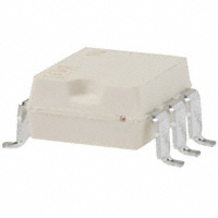
Series PVT212PbF
Microelectronic Power IC
®
HEXFET Power MOSFET Photovoltaic Relay
Single-Pole, Normally-Open, 0-150V, 550mA AC / 825mA DC
General Description
The PVT212 Series Photovoltaic Relay is a singlepole, normally open solid-state relay that can replace
electromechanical relays in many applications. It
utilizes International Rectifier’s proprietary HEXFET
power MOSFET as the output switch, driven by an
integrated circuit photovoltaic generator of novel
construction. The output switch is controlled by
radiation from a GaAlAs light emitting diode (LED)
which is optically isolated from the photovoltaic
generator.
These SSRs are specifically designed for industrial
control and peripheral telecom applications. Series
PVT212 Relays are packaged in a 6-lead molded
DIP package with either thru-hole or surface mount
(‘gull-wing’) terminals. It is available in standard
plastic shipping tubes or on tape-and-reel. Please
refer to part identification information.
Features
HEXFET Power MOSFET output
Bounce-free operation
4,000 VRMS I/O isolation
Very low on-resistance (RDD-ON)
Linear AC/DC operation
Solid-State Reliability
UL recognized
ESD Tolerance:
4000V Human Body Model
500V Machine Model
.
Applications
Control of AC (up to 90 VAC) industrial
loads
Control of DC industrial loads up to
+/-120 VDC
Telecom line switching
Part Identification
PVT212PbF
PVT212SPbF
PVT212S-TPbF
thru-hole
surface-mount
surface-mount, Tape and Reel
(HEXFET is the registered trademark for International Rectifier Power MOSFETs)
1
www.irf.com © 2015 International Rectifier
Submit Datasheet Feedback
May 18, 2015
�Series PVT212PbF
Electrical Specifications (TA = +25°C unless otherwise specified)
INPUT CHARACTERISTICS
Limits
Units
Minimum Control Current (see figure 1)
Maximum Control Current for Off-State Resistance
Control Current Range (Caution: current limit input LED, see figure 5)
5.0
0.4
5.0 to 25
mA
mA
mA
6.0
V
Maximum Reverse Voltage
OUTPUT CHARACTERISTICS
Operating Voltage Range
Maximum Load Current @ TA=+40°C 5mA Control (see figure 1)
A Connection
B Connection
C Connection
Maximum On-State Resistance @TA=+25°C
100mA Pulsed Load, 5mA Control (see figures 2 & 3)
A Connection
B Connection
C Connection
Max. pulsed Load Current @TA=+25°C, 10mA Control (10mS @ 10% duty cycle)
Maximum Off-State Leakage @TA=+25°C, ±150V
Maximum Turn-On Time @TA=+25°C (see figures 6 & 7)
For 50mA, 100 V DC load, 10mA Control (5mS pulse width @ 50% duty cycle)
Maximum Turn-Off Time @TA=+25°C (see figures 6 & 7)
For 50mA, 100 V DC load, 10mA Control (5mS pulse width @ 50% duty cycle)
Maximum Output Capacitance @ 50VDC, f=1MHz (Cout, see figure 8)
GENERAL CHARACTERISTICS
Minimum Dielectric Strength, Input-Output
Minimum Insulation Resistance, Input-Output
Maximum Capacitance, Input-Output Vd=0V, f=1MHz
Maximum Pin Soldering Temperature (10 seconds maximum)
Ambient Temperature Range:
Operating
Storage
Limits
Units
0 to ±150
V peak
550
600
825
mA
mA
mA
0.75
0.40
0.25
1200
1.0
Ω
Ω
Ω
mA
µA
3.0
ms
0.5
100
ms
pF
Limits
Units
4000
1012
1.0
+260
-40 to +85
-40 to +100
VRMS
Ω
pF
°C
International Rectifier does not recommend the use of this product in aerospace, avionics, military or life support applications.
Users of this International Rectifier product in such applications assume all risks of such use and indemnify International
Rectifier against all damages resulting from such use.
Connection Diagrams
2
www.irf.com © 2015 International Rectifier
Submit Datasheet Feedback
May 18, 2015
�Series PVT212PbF
700
ILED = 5mA
“A” Connection
“A” Connection
2.0
1.5
ILED=3mA
500
1.0
Load Current (mA)
Max Load Current (mA)
600
400
300
0.5
0.0
-1.0
-0.8
-0.6
-0.4
-0.2
0.0
0.2
-1.0
200
-1.5
100
0.4
0.6
0.8
1.0
-0.5
I LED = 5mA
10mS Pulsed, 25C
-2.0
Voltage Drop (VDD)
0
0
20
40
60
80
100
Ambient Temperature (C)
Figure 2. Typical On Characteristics
Figure 1. Typical Current Derating Curves
1.4
“A” Connection
I LED = 5mA
1.2
Load Current (A)
1.0
10mS - Pulsed, 25ºC
25ºC
40ºC
60ºC
85ºC
0.8
0.6
0.4
0.2
0.0
0.0
3
0.1
0.2
0.3
0.4
0.5
0.6
0.7
VDD (Volts) Ambient
Ambient Temperature (oC)
Figure 3. Typical On-Characteristics
Figure 4. Typical Normalized Off-State Leakage
www.irf.com © 2015 International Rectifier
Submit Datasheet Feedback
May 18, 2015
�Series PVT212PbF
10.0
“A” Connection
Delay Time (mS)
max. device
& -45°C lim
it
TYPICAL
min. devic
e & +85°C
limit
Input Current (mA)
Ton
Tdly
1.0
Toff
0.1
0
0.5
1.0
1.5
0
2.0
5
10
15
I LED (mA)
LED Forward Voltage Drop (Volts DC)
Figure 6. Typical Delay Times
(5mS Pulse Width, 100V/50mA Load)
Figure 5. Input Characteristics (Current Controlled)
800
“A” Connection
700
Typical Capacitance (pF)
600
ILED
90%
500
400
300
200
I
D
10%
100
tdly
ton
toff
0
0
10
20
30
40
50
60
70
80
90
100
VDD Drain to Drain Voltage
Figure 7. Delay Time Definitions
4
www.irf.com © 2015 International Rectifier
Figure 8. Typical Output Capacitance
Submit Datasheet Feedback
May 18, 2015
�Series PVT212PbF
Case Outlines
01-2008 01
01-2009 01
Note: For the most current drawing please refer to IR website at: http://www.irf.com/package/
5
www.irf.com © 2015 International Rectifier
Submit Datasheet Feedback
May 18, 2015
�Series PVT212PbF
Qualification information
Qualification level
Moisture Sensitivity
Level
RoHS compliant
†
Industrial
††
(per JEDEC JESD47I guidelines)
PVT212PbF
N/A
PVT212SPbF
MSL4
††
PVT212S-TPbF
(per JEDEC J-STD-020E & JEDEC J-STD-033C )
Yes
† Qualification standards can be found at International Rectifier’s web site: http://www.irf.com/product-info/reliability
†† Applicable version of JEDEC standard at the time of product release
Revision History
Date
5/18/2015
Comments
• Added Qualification Information Table on page 6
• Updated data sheet with new IR corporate template
IR WORLD HEADQUARTERS: 101 N. Sepulveda Blvd., El Segundo, California 90245, USA
Data and specifications subject to change without notice
To contact International Rectifier, please visit http://www.irf.com/whoto-call/
6
www.irf.com © 2015 International Rectifier
Submit Datasheet Feedback
May 18, 2015
�
很抱歉,暂时无法提供与“PVT212S”相匹配的价格&库存,您可以联系我们找货
免费人工找货- 国内价格 香港价格
- 100+45.98273100+5.95638