Revision 2.4, 2015-10-20
�Edition 2015-10-20
Published by
Infineon Technologies AG
81726 Munich, Germany
© 2015 Infineon Technologies AG
All Rights Reserved.
Legal Disclaimer
The information given in this document shall in no event be regarded as a guarantee of conditions or
characteristics. With respect to any examples or hints given herein, any typical values stated herein and/or any
information regarding the application of the device, Infineon Technologies hereby disclaims any and all
warranties and liabilities of any kind, including without limitation, warranties of non-infringement of intellectual
property rights of any third party.
Information
For further information on technology, delivery terms and conditions and prices, please contact the nearest
Infineon Technologies Office (www.infineon.com).
Warnings
Due to technical requirements, components may contain dangerous substances. For information on the types in
question, please contact the nearest Infineon Technologies Office.
Infineon Technologies components may be used in life-support devices or systems only with the express written
approval of Infineon Technologies, if a failure of such components can reasonably be expected to cause the
failure of that life-support device or system or to affect the safety or effectiveness of that device or system. Life
support devices or systems are intended to be implanted in the human body or to support and/or maintain and
sustain and/or protect human life. If they fail, it is reasonable to assume that the health of the user or other
persons may be endangered.
�PX3517
Revision History
Page or Item
Subjects (major changes since previous revision)
Revision 2.2
2014-03-262015-10-20 Conditions for RT pin not used
table 2: pin RT description
paragraph 5.5 Thermal Protection description
Revision 2.3
2014-10-13
RPHASE added in the Simplified Block Diagram
SOA diagram for RPHASE introduced
Revision 2.4
2015-10-20
Power up and power down sequence introduced
Junction operating temperature from -25°C to -40°C table 1 and table 7
Trademarks of Infineon Technologies AG
AURIX™, BlueMoon™, COMNEON™, C166™, CROSSAVE™, CanPAK™, CIPOS™, CoolMOS™,
CoolSET™, CORECONTROL™, DAVE™, EasyPIM™, EconoBRIDGE™, EconoDUAL™, EconoPACK™,
EconoPIM™, EiceDRIVER™, EUPEC™, FCOS™, HITFET™, HybridPACK™, ISOFACE™, I²RF™,
IsoPACK™, MIPAQ™, ModSTACK™, my-d™, NovalithIC™, OmniTune™, OptiMOS™, ORIGA™, PROFET™,
PRO-SIL™, PRIMARION™, PrimePACK™, RASIC™, ReverSave™, SatRIC™, SIEGET™, SINDRION™,
SMARTi™, SmartLEWIS™, TEMPFET™, thinQ!™, TriCore™, TRENCHSTOP™, X-GOLD™, XMM™,
X-PMU™, XPOSYS™.
Other Trademarks
Advance Design System™ (ADS) of Agilent Technologies, AMBA™, ARM™, MULTI-ICE™, PRIMECELL™,
REALVIEW™, THUMB™ of ARM Limited, UK. AUTOSAR™ is licensed by AUTOSAR development
partnership. Bluetooth™ of Bluetooth SIG Inc. CAT-iq™ of DECT Forum. COLOSSUS™, FirstGPS™ of Trimble
Navigation Ltd. EMV™ of EMVCo, LLC (Visa Holdings Inc.). EPCOS™ of Epcos AG. FLEXGO™ of Microsoft
Corporation. FlexRay™ is licensed by FlexRay Consortium. HYPERTERMINAL™ of Hilgraeve Incorporated.
IEC™ of Commission Electrotechnique Internationale. IrDA™ of Infrared Data Association Corporation. ISO™
of INTERNATIONAL ORGANIZATION FOR STANDARDIZATION. MATLAB™ of MathWorks, Inc. MAXIM™ of
Maxim Integrated Products, Inc. MICROTEC™, NUCLEUS™ of Mentor Graphics Corporation. Mifare™ of NXP.
MIPI™ of MIPI Alliance, Inc. MIPS™ of MIPS Technologies, Inc., USA. muRata™ of MURATA
MANUFACTURING CO., MICROWAVE OFFICE™ (MWO) of Applied Wave Research Inc., OmniVision™ of
OmniVision Technologies, Inc. Openwave™ Openwave Systems Inc. RED HAT™ Red Hat, Inc. RFMD™ RF
Micro Devices, Inc. SIRIUS™ of Sirius Sattelite Radio Inc. SOLARIS™ of Sun Microsystems, Inc. SPANSION™
of Spansion LLC Ltd. Symbian™ of Symbian Software Limited. TAIYO YUDEN™ of Taiyo Yuden Co.
TEAKLITE™ of CEVA, Inc. TEKTRONIX™ of Tektronix Inc. TOKO™ of TOKO KABUSHIKI KAISHA TA.
UNIX™ of X/Open Company Limited. VERILOG™, PALLADIUM™ of Cadence Design Systems, Inc. VLYNQ™
of Texas Instruments Incorporated. VXWORKS™, WIND RIVER™ of WIND RIVER SYSTEMS, INC. ZETEX™
of Diodes Zetex Limited.
Last Trademarks Update 2010-06-09
Datasheet
3
Revision 2.4, 2015-10-20
�PX3517
Applications
1
Applications
Desktop and Server VR11.X and VR12.X
VR12 .X Vcore and non-Vcore
non Vcore buck
buck-converter
converters
converters
Network and Telecom
elecom uncontrolled processor VR
Single Phase and Multiphase POL
CPU/
CPU/GPU
GPU Regulation in Graphics Cards and Gaming Consoles
Voltage Regulator Modules requiring high power density
Memory (DDR2/3)
2
Features
High frequency operation up to 1.2
1.2MHz
MHz
Capability to drive MOSFET at 50A
0A continuous current per phase
Wide
ide driving input voltage range from 4.5V to 9V
Adjustable thermal warning
Thermal warning report function
Wide input voltage range:
r ange: up to 16V
16
Low power dissipation
Includes bootstrap diode
Adaptive shoot through protection
Compatible with standard +3.
+3.3
3V
V PWM co
controller
ntroller ICs
Tri
Tri-state
state PWM input functionality
Small package: 3mm x 3mm TDSON-10
TDSON 0
RoHS compliant
Table 1
Product Identification
Identification
Part Number
PX3517
Figure 1
Datasheet
Temperature
Temp
erature Range
40 to 125C
125 C
-40
Package
3x
TDSON
DSON 10
x3
3 10-leads
10 leads T
DSON-10
Marking
3517
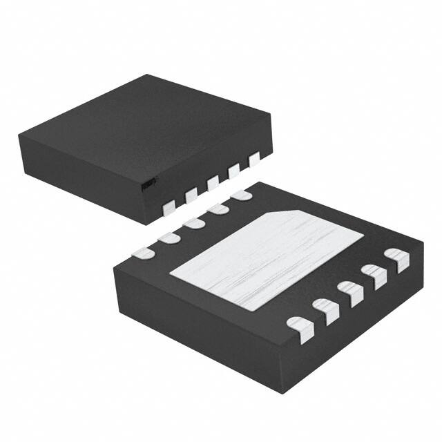
Picture of the product
4
20
Revision 2.4,
2.4 2015-10
2015 10-20
�PX3517
Description
3
Description
3.1
Pinout
Figure 2
Pinout, numbering and pin names (transparent top view)
Note: Signals marked with “#” are active low.
Table 2
Pin No.
I/O Signals
Name
Pin Type Buffer Type Function
1
UGATE
O
Analog
Upper gate drive output
Connect to high side N-channel power MOSFET gate.
2
BOOT
O
Analog
Floating bootstrap supply pin for upper gate drive
1
Connect the bootstrap capacitor between this pin and the
PHASE pin. The bootstrap capacitor provides the charge to
turn on the upper MOSFET. See the Internal Bootstrap
Device section herein for guidance in choosing the
capacitance value.
3
THW#
O
Analog
Open drain output
2
Connect this pin to 3.3V through a resistor . Once the
thermal protection threshold is tripped, the THW# pin is
pulled down. Leave open if not used.
4
PWM
I
3.3V Logic
PWM drive logic input
Connect this pin to the PWM out from the controller IC.
6
LGATE
O
Analog
Lower gate drive output
Connect to low side N-channel power MOSFET gate.
8
RT
O
Analog
Thermal warning threshold selection pin
Connect this pin to an external resistance2 to GND. Used
to set the thermal warning threshold. If not used it can be
left floating.
10
PHASE
I
Analog
Return path for high side MOSFET driver
Connect this pin to the source of the upper MOSFET and
the drain of the lower MOSFET. This pin provides a return
path for the upper gate drive.
1
2
See section 5.2 for guidance in choosing capacitance value
See section 5.5 for resistor value selection
Datasheet
5
Revision 2.4, 2015-10-20
�PX3517
Description
Table 3
Pin No.
Power Supply
Name
Pin Type Buffer Type Function
7
VCC
POWER
-
Supply for IC housekeeping and logic
Connect to +4.5V-8V power supply. Place a high quality low
ESR ceramic capacitor from this pin to GND.
9
PVCC
POWER
-
Supply for IC driver section
Connect this pin to +4.5V-8V power supply.
Table 4
Pin No.
Ground Pins
Name
Pin Type Buffer Type Function
5
GND
GND
-
GND connection
Can be left open since main GND connection to circuit
board is established by die pad. Cannot be used as sole
ground connection (does not replace die pad ground).
-
Die Pad
GND
-
Bias and reference ground
All signals are referenced to this node. It is also the power
ground return for the driver. It is mandatory to connect the
die paddle electrically and thermally to the circuit board.
3.2
General Description
The PX3517 is a dual, high speed driver designed to drive a wide range of high side and low side N-channel
power MOSFETs in synchronous rectified buck converters. When combined with the Primarion family of Digital
Multi-phase Controller ICs or Digital Point of Load Controller ICs and Infineon N-channel MOSFET products, the
PX3517 forms a complete core-voltage regulator solution for advanced micro and graphics processors as well
as point-of-load applications. VCC and PVCC can be tied together and supplied by a voltage ranging between
4.5V and 8V. They can be separated for better noise decoupling of the logic section (VCC) from the power
section (PVCC). They can also be supplied with different voltages, but in this case the appropriate power
up/down sequence has to be implemented. PVCC provides the capability of driving the high side MOSFET gate
and low side MOSFET gate with a variable gate driving voltage to tailor efficiency based on customer
conditions. Adaptive shoot-through protection is integrated into the IC. This prevents both upper and lower
MOSFETs from conducting simultaneously and minimizes dead time. A thermal warning function with an
adjustable threshold, set by an external resistance, is featured to protect the system from thermal issues. Once
the junction temperature of the PX3517 encounters the thermal warning threshold the driver outputs a logic
signal through the open drain THW# pin.
Datasheet
6
Revision 2.4, 2015-10-20
�PX3517
Description
Figure 3
Datasheet
Simplified block diagram
7
Revision 2.4, 2015-10-20
�PX3517
Electrical specification
4
Electrical specification
4.1
Absolute Maximum Ratings
Stresses above those listed in Table 5 “Absolute Maximum Ratings” may cause p
permanent
ermanent damage to the
device. These
These are
are absolute
absolute stress
stress ratings
ratings only
only and
and operation
operation of
of the
the device
device is
is not
not implied
implied or
or recommended
recommended at
at
these or any other conditions
conditions in excess of those given in the operational sections
s ections of this specification. Exposure
to
to the
the absolute
absolute maximum
maximum ratings
ratings for
for extended
extended periods
periods may
may adversely
adversely affect
affect the
the operation
operation and
and reliability
reliability of
of the
the
device.
Table 5
Absolute Maximum Ratings (Tambient =25°C)
Parameter
Symbol
Values
Unit
Min.
Typ.
Max.
VCC PVCC supply voltage (DC) VVCC,
VCC VPVCC
--0.3
0.3
9
V
Note / Test
Conditions
Condition
THW#
THW#
--0.3
0.3
–
–
3.6
V
BOOT voltage
VBOOT
--0.3
0.3
–
30
V
BOOT to PHASE voltage
VBOOT - VPHASE
--0.3
0.3
–
9
V
--1
--8
–
–
–
16
25
V
V
–
3.6
V
–
–
V
--40
–
3.6
150
C
–
--55
–
150
C
–
PHASE voltage, DC
PHASE voltage, pulsed
VPHASE
VPHASE
VPWM
RT
Junction temperature
VRT
T Jmax
T
Storage temperature
3
3)
TTB
TB
T STG
T
TTB
TB
3))
The pulse duration is 10ns.
Typical server VCORE
application conditions
Figure 4
Datasheet
Safe Operating Area of R PHASE
8
20
Revision 2.4,
2.4 2015-10
2015 10-20
�PX3517
Electrical specification
Note: ton refers to the on-time of the HS-MOSFET. For input voltages below 12 V no limits on the duration of t on
need to be applied.The relative position of a typical Server VCORE application conditions V IN=12V
VOUT=1.8V fSW=450kHz is represented as reference.This Safe Operating Area is verified by design, not
100% tested in production.
Note: All rated voltages are relative to voltages on the GND pins unless otherwise specified.
Datasheet
9
Revision 2.4, 2015-10-20
�PX3517
Electrical specification
4.2
Thermal Characteristics
Table 6
Thermal Characteristics
Parameter
Symbol
Values
Thermal resistance, junction-soldering
3
point
θJS
-
7
-
Thermal resistance, junction-top of
package
θJtop
-
20
-
Min.
4.3
Typ.
Unit
Note / Test Condition
K/W
-
Max.
-
Recommended Operating Conditions and Electrical Characteristics
Note: PVCC = VCC = 5V, Tambient = 25°C
Table 7
Recommended Operating Conditions
Parameter
Symbol
MOSFET driver voltage
Logic supply voltage
T
Unit
Min.
Typ.
V PVCC
4.5
-
8.0
V VCC
4.5
-
8.0
TTB
TB
T
Values
TTB
TB
Test conditions
Max.
V
–
–
rising edge between 3.1V and 4.5V :
dvCC/dt>5V/100ms
Frequency of the PWM
Junction temperature
fSW
T jOP
T
TTB
TB
-40
1.2
MHz
Note4
+125
°C
–
Minimum on time
20
ns
Note4
Minimum off time
30
ns
Note4
Table 8
Voltage Supply And Biasing Current
Parameter
Symbol
Values
Unit
Test conditions
Min.
Typ.
Max.
VUVLO_R
-
3.6
4.5
UVLO falling
VUVLO_F
-
3.2
-
Driver current
IPVCC_300kHz
-
2
-
mA
fSW = 300kHz
IPVCC_PWML
-
670
-
μA
PWM = 0V
IVCC_PWML
-
1.05
-
mA
PWM = 0V
IVCC_O
-
660
-
μA
PWM = Open
UVLO rising
V
VCC rising
rising edge between 3.1V and 4.5V :
dvCC/dt>5V/100ms
IC current (control)
3
VCC falling
The junction-soldering point is referred to the GND bottom exposed pad.
Datasheet
10
Revision 2.4, 2015-10-20
�PX3517
Electrical specification
Table 9
Logic Inputs And Threshold
Parameter
Symbol
Values
Min.
THW#
Programmable
Warning
Temperature range
PWM
Typ.
70
Thermal warning
accuracy
Unit
–
Max.
130
°C
-10
–
+10
Hysteresis
–
10
–
On resistance
–
37.5
80
Ω
Leakage current
–
0.1
5
μA
0.8
V
Input low
Input high
Input resistance
Open voltage
Tri-state shutdown
window
T
T
T
T
T
V PWM_L
–
2.5
–
–
-
2.06
–
kΩ
–
1.6
–
V
TB
V PWM_H
TTB
TB
R IN-PWM
TTB
V PWM_O
TB
TTB
V PWM_S
TB
TTB
TB
ILOAD = 8mA
–
TTB
1.2
–
Test conditions
T
V PWM falling
TTB
TB
T
V PWM rising
TTB
TB
T
TTB
TB
T
2.0
V PWM = 1 V
V PWM_O
TTB
TB
–
TPFPT
Table 10
Timing Characteristics
Parameter
Symbol
Values
Min.
Typ.
Unit
Test conditions
Max.
Upper Gate (UGATE) Output
Shutdown hold off time
UGATE rise time
UGATE fall time
Tri-state to high propagation
delay
UGATE turn-on propagation
delay
UGATE turn-off propagation
delay
tSSHD_U
50
tr_U
10
Note4, 3nF load
tf_U
10
Note4, 3nF load
tPDTS_U
15
No load
tPDH_U
15
No load
tPDL_U
20
No load
tSSHD_L
50
tr_L
10
ns
No load
Lower Gate (LGATE) Output
Shutdown hold-off time
LGATE rise time
LGATE fall time
Tri-state to low propagation
delay
LGATE turn-on propagation
delay
LGATE turn-off propagation
delay
ns
No load
Note4, 3nF load
tf_L
5
Note4, 3nF load
tPDTS_L
15
No load
tPDH_L
15
No load
tPDL_L
7
No load
Thermal warning
Thermal warning propagation
delay
4
tD_THW#
10
s
Parameter verified by design, not 100% tested in production.
Datasheet
11
Revision 2.4, 2015-10-20
�PX3517
Electrical specification
Table 11
Output Characteristics
Parameter
Symbol
Values
Min.
Typ.
Unit
Test conditions
Max.
Output Characteristics
Upper drive source current
ISRC_UG
2
A
Note4, current pulse < 20ns
Upper drive source impedance
RSRC_UG
0.8
Ω
ISRC_UG = 200mA
Upper drive sink current
ISNK_UG
2
A
Note4, current pulse < 20ns
Upper drive sink impedance
RSNK_UG
0.6
Ω
ISINK_UG = 200mA
Lower drive source current
ISRC_LG
2
A
Note4, current pulse < 40ns
Lower drive source impedance
RSRC_LG
0.8
Ω
ISRC_UG = 200mA
Lower drive sink current
ISNK_LG
4
A
Note4, current pulse < 40ns
Lower drive sink impedance
RSNK_LG
0.35
Ω
ISINK_UG = 200mA
Datasheet
12
Revision 2.4, 2015-10-20
�PX3517
Theory of Operation
5
Theory of Operation
The PX3517 functionality is enabled by the VCC pin. When the VCC pin voltage overcomes the VCC rising
voltage threshold, the driver begins to operate depending on the PWM status. Before the VCC pin voltage
voltage reaches the VCC rising threshold both MOSFETs are kept in the OFF state. For VCC is recommended
to have a slope for the rising edge higher than 5V/100ms around the rising UVLO threshold.
The PX3517 functionality is driven by PWM signal transitions. When the PWM signal performs a transition from
low state to high state (PWM voltage higher than 2.5V typ) the low side MOSFET is turned off, after the turn off
propagation delay time. Next the high side MOSFET is turned on, after the turn on propagation delay time. Once
the on time has expired, the PWM signal provides a transition from high state to low state (PWM voltage lower
than 0.8V typ). This will drive the high side MOSFET from the ON state to the OFF state, after the turn off
propagation delay time. The PX3517 is also capable of driving two external MOSFETs into the OFF state. When
the PWM signal level enters the shut down window or tri-state (typically between 1.2V and 2V), after the shut
down hold off time has expired, both MOSFETs are switched off. This feature is useful when the IC controller
wants to reduce the number of active phases in order to decrease power consumption. In principle the tri-state
can also be used to improve performance during transitions between heavy and light loads.
The PX3517 implements an embedded resistor network, which forces the PWM pin voltage of the device into
the middle of the shut down window if the PWM input is left floating by the controller IC.
An adaptive anti-shoot-through control scheme is implemented in order to avoid cross conduction between the
high side MOSFET and the low side MOSFET. This adaptive scheme allows for the use of a variety of different
power MOSFETs for different kinds of power conversion. Nevertheless, the dead time is kept as short as
possible in order to maximize the efficiency of the overall solution.
The adaptive cross conduction protection is based on the gate-to-source voltage level of the MOSFETs during
turn off. When the PWM signal goes low, the high side MOSFET will begin to turn off. Once the V GS of the high
side MOSFET is discharged below 1V, the low side MOSFET will begin to turn on.
When the PWM signal goes high, the low side MOSFET will begin to turn off. Once the V GS of the low side
MOSFET is discharged below 1V, the high side MOSFET will begin to turn on.
There is an additional control mechanism on the PHASE pin that forces the turn on of the low side MOSFET if
the PHASE pin is not actively held high. This ensures that the converter will sink current efficiently, and that the
bootstrap capacitor will be refreshed appropriately during each switching cycle.
During start up it is possible for the 12V conversion input to rise before the 5V input. In this case, the high side
MOSFET can have an induced turn on through the CGD/CGS partition. In order to avoid this undesirable effect
the PX3517 embeds a resistance of 10k between UGATE pin and PHASE pin.
The PX3517 features adjustable thermal warning protection. The thermal warning trip point ranges from 70°C to
130°C, and is selected according to a resistance between the RT pin and GND pin. An embedded thermal
sense element senses the driver temperature and compares it to the trip point. Once the two temperatures
match, a logical signal is issued by the THW# pin. In this case the driver system does not shut down. The
thermal warning has a hysteresis of 10°C. Once the temperature reaches the threshold determined by the
external resistance, the THW# will be de-asserted if the temperature drops below the threshold by 10°C.
5.1
Driver Characteristics
The gate driver of the PX3517 has 2 voltage inputs, VCC and PVCC. VCC is the logic supply for the driver.
PVCC is used to drive the high and low side MOSFETs. Ceramic capacitors should be placed very close to
these input voltage pins to decouple the sensitive control circuitry from a noisy environment.
Since two different pins are provided for supplying the power to the driver, the correct power up/down sequence
has to be considered. In order to avoid false turn on of the gates (spurious high side turn on, for instance) it is
strongly suggested to ensure that the voltage at the VCC pin reaches the UVLO threshold earlier than the
PVCC pin. In this way the logic section will ensure the correct functionality of the power section.
Proper response of the driver to the PWM signal is only guaranteed when UVLO have been cleared by the
respective supply voltages (ref to table 8).
Datasheet
13
Revision 2.4, 2015-10-20
�PX3517
Theory of Operation
Therefore, it is strongly recommended to only issue pulses to PWM when no UVLO conditions are present. The
power down sequence should set PWM to HiZ with respect the internal threshold, before ramping down VIN
(see figure 7 for VIN connection), PVCC and VCC respectively.
The MOSFETs selected for this application are optimized for 5V gate drive, giving the end user optimized
efficiency at both high load and light load. Nevertheless the driving voltage (PVCC) can be increased,
(independently from VCC), up to 8V in order to have a customized efficiency curve depending on application
conditions. The reference for the power circuitry including the driver output stage and the reference for the gate
driver control circuit is CGND.
Referring to the block diagram in Figure 3 on page 7, VCC is internally connected to the UVLO circuit. For VCC
voltages less than the 3.6V (typ.) required for proper circuit operation, the UVLO circuit will perform a system
shut-down. PVCC supplies both the floating high side MOSFET driver and the low side MOSFET driver circuits.
An active boot circuit for the high side MOSFET gate drive is also included. A second UVLO circuit, sensing the
BOOT voltage level, is implemented to prevent false UGATE turn on during insufficient power supply level
conditions (BOOT Cap charging/discharging sequence). During such an undervoltage condition both UGATE
and LGATE are driven low actively. Further, a passive pull-down (10k) is placed on each gate.
UVLO Output
Logic Level
“H”
Enable
Shutdown
“L”
VUVLO_F
VUVLO_R
Figure 5
Internal output signal from UVLO unit
5.2
Current Capability and Internal Bootstrap
VCC
The PX3517 implements high current capability and low ohmic pull down resistances for the driving stages. The
high current capability ensures fast switching transition for the MOSFETs. This reduces the switching losses
(2A of driving source/sink current for the upper MOSFET) even with high gate charge high side MOSFETs. The
low ohmic pull down resistance (lower drive sink impedance 0.35) prevents induced turn on phenomenon of
the low side MOSFET during the fast turn on of the high side MOSFET.
The high side MOSFET is powered through the bootstrap circuitry. The PX3517 provides an embedded
bootstrap diode, so to complete the power network only a capacitance between the PHASE pin and the BOOT
pin is needed. In many cases the PX3517 is optimized for the best switching behavior, so an external resistance
is not needed. The bootstrap capacitance is chosen depending on the high side MOSFETgate charge. The
following formula gives a good estimation of the voltage drop across the bootstrap capacitance due to the
charging of the high side MOSFET.
VBOOT is the desired variation of the bootstrap voltage. This should generally be as low as possible in order
to avoid high side MOSFET RDSON drop. Generally, a value between 0.1V and 0.01V is acceptable.
The low side MOSFET driver is powered through the PVCC pin. The same considerations and formula for the
bootstrap capacitance can be applied to the capacitance used to filter the PVCC pin.
The flexibility to adjust the driving voltage from 4.5V to 8V gives designers the capability to shape the efficiency
curve in any way that is desired.
Datasheet
14
Revision 2.4, 2015-10-20
�PX3517
Theory of Operation
5.3
Power Dissipation
The power dissipation of the driver is given by the gate charge of the external power MOSFETs. The following
formulas held:
fSW is the switching frequency and QGHS and QGLS are respectively the gate charge of the high side MOSFET
and the gate charge of the low side MOSFET at the PVCC driving voltage. The very low thermal resistance
package used for the PX3517 allows the device to avoid any usage of external resistances to decrease the
power dissipation inside the driver even with high driving voltage. Since the thermal resistance is strongly
influenced by the number of layers used in the board, it is recommended to roughly check the expected junction
temperature via the power calculation.
5.4
Inputs to the Internal Control Circuits
The PWM is the control input to the IC from an external PWM controller IC and is compatible with 3.3V.
The PWM input has tri-state functionality. When the voltage remains in the specified PWM shutdown window for
at least the PWM shutdown holdoff time t_tsshd, operation is suspended by keeping both MOSFET gate outputs
low. If left open, the pin is internally fixed to VPWM_O = +1.6V level.
During the power-up sequence, the initial state of the PWM signal is ignored, until the first rising edge.
Since all the thresholds are derived from an internal linear regulator they will not depend on the VCC input.
Table 12
PWM Pin Functionality
PWM logic level
Driver output
Low
LGATE= High, UGATE = Low
High
LGATE = Low, UGATE = High
Open (left floating, or High impedance)
LGATE = Low, UGATE = Low
5.5
Thermal Protection
The THW# pin offers the possibility to check when the temperature of the driver overcomes the threshold fixed
by the RT pin resistor. Once the temperature of the driver matches the trip point this open drain output (pulled
up to 3.3V by, for instance, an external resistance in the range of 10k) is pulled to zero (active low) with a
typical resistance of 37. When the temperature of the device goes below the thermal warning minus the
hysteresis (10°C typ), the pin THW# is released and pulled up by the external resistance. If the thermal warning
is not used, then leave the pin floating. The thermal warning protection does not switch off the driver.
TWH# Output
Logic Level
“H”
“L”
TTHW#_FALLING
Figure 6
TTHW#_RAISING
Tj
Thermal warning
The RT pin provides the option to program the trip point of the thermal warning as follows:
Datasheet
15
Revision 2.4, 2015-10-20
�PX3517
Theory of Operation
T is the desired warning temperature. If the threshold is fixed to T=100°C then the T is 30°C and external
resistance is equivalent to 89.5k, as shown in the following table.
Desired warning temperature [°C]
70
80
90
100
110
120
130
Resistance connected to the RT pin []
82000
84400
87000
89500
92000
94400
96880
The adjustability of the thermal warning should compensate the fact that the sensing point on the driver can be
slightly different from the hot spot of the application. In this case a gap between the temperature of the hot spot
and the temperature of the driver can be measured and then the thermal warning can be designed with an offset
to compensate for the difference.
In order to have better temperature matching it is strongly recommended to connect the GND exposed pad of
the driver as near as possible to the hot spot.
If the thermal protection is not used the RT pin can be left floating.
5.6
Layout Considerations
The PX3517 has a good protection system against unwanted overshoot and undershoot; the PHASE pin can
range between dynamically from -8V to 25V.
The parasitic inductances of the PCB and of the power devices’ packaging (both upper and lower MOSFETs)
can cause serious ringing, exceeding absolute maximum rating of the devices. Careful layout can help minimize
such unwanted stress. The following advice is meant to lead to an optimized layout:
Keep decoupling loops (PVCC-GND and BOOT-PHASE) as short as possible.
Minimize trace inductance, especially on low impedance lines. All power traces (UGATE, PHASE, LGATE,
GND, PVCC) should be short and wide, as much as possible.
The PHASE node should also be short and wide. Minimize the distance between the PHASE node and both the
high side MOSFET source and the low side MOSFET drain to avoid efficiency losses.
Minimize the current loop of the output and input power trains. Short the source connection of the lower
MOSFET to ground as close to the transistor pin as feasible. Input capacitors (especially ceramic decoupling)
should be placed as close to the drain of upper and source of lower MOSFETs as possible.
To optimize heat spreading, copper should be placed directly underneath the IC whether it has an exposed pad
or not. The copper area can be extended beyond the bottom area of the IC and/or connected to buried copper
plane(s) with thermal vias. This combination of vias for vertical heat escape, extended copper plane, and buried
planes for heat spreading allows the IC to achieve its full thermal potential.
Datasheet
16
Revision 2.4, 2015-10-20
�PX3517
Application
6
Application
Figure 7
Pin interconnection outline (transparent top view)
7
Gate Driver Timing Diagram
1.2V