SPA06N60C3
CoolMOSTM Power Transistor
Product Summary
Features
• New revolutionary high voltage technology
• Ultra low gate charge
V DS @ T j,max
650
V
R DS(on),max
0.75
Ω
I D1)
6.2
A
• Periodic avalanche rated
• High peak current capability
• Ultra low effective capacitances
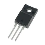
P-TO220-3-31
• Extreme dv /dt rated
• Improved transconductance
• Fully isolated package (2500 V AC; 1 minute)
Type
Package
Ordering Code
Marking
SPA06N60C3
PG-TO220-3-31
Q67040-S4631
06N60C3
Maximum ratings, at T j=25 °C, unless otherwise specified
Parameter
Symbol Conditions
Continuous drain current 1)
ID
Value
T C=25 °C
6.2
T C=100 °C
3.9
Pulsed drain current1)
I D,pulse
T C=25 °C
18.6
Avalanche energy, single pulse
E AS
I D=3.1 A, V DD=50 V
200
Avalanche energy, repetitive t AR1),2)
E AR
I D=6.2 A, V DD=50 V
0.5
Avalanche current, repetitive t AR1)
I AR
Drain source voltage slope
dv /dt
Gate source voltage
Unit
A
mJ
6.2
A
I D=6.2 A, V DS=480 V,
T j=125 °C
50
V/ns
V GS
static
±20
V
V GS
AC (f >1 Hz)
±30
Power dissipation
P tot
T C=25 °C
32
W
Operating and storage temperature
T j, T stg
-55 ... 150
°C
Rev. 1.3
Rev 1.4
page 1
1
2010-12-21
2017-08-17
�SPA06N60C3
Parameter
Values
Symbol Conditions
Unit
min.
typ.
max.
-
-
3.92
Thermal characteristics
Thermal resistance, junction - case
R thJC
Thermal resistance, junction ambient
R thJA
leaded
-
-
80
Soldering temperature
T sold
1.6 mm (0.063 in.)
from case for 10 s
-
-
260
°C
600
-
-
V
-
700
-
K/W
Electrical characteristics, at T j=25 °C, unless otherwise specified
Static characteristics
Drain-source breakdown voltage
V (BR)DSS V GS=0 V, I D=250 µA
Avalanche breakdown voltage
V (BR)DS
V GS=0 V, I D=6.2 A
Gate threshold voltage
V GS(th)
V DS=V GS, I D=0.26 mA
2.1
3
3.9
Zero gate voltage drain current
I DSS
V DS=600 V, V GS=0 V,
T j=25 °C
-
0.1
1
V DS=600 V, V GS=0 V,
T j=150 °C
-
-
100
µA
Gate-source leakage current
I GSS
V GS=20 V, V DS=0 V
-
-
100
nA
Drain-source on-state resistance
R DS(on)
V GS=10 V, I D=3.9 A,
T j=25 °C
-
0.68
0.75
Ω
V GS=10 V, I D=3.9 A,
T j=150 °C
-
1.82
-
Gate resistance
RG
f =1 MHz, open drain
-
1
-
Transconductance
g fs
|V DS|>2|I D|R DS(on)max,
I D=3.9 A
-
5.6
-
Rev. 1.3
Rev 1.4
page 2
2
S
2010-12-21
2017-08-17
�SPA06N60C3
Parameter
Values
Symbol Conditions
Unit
min.
typ.
max.
-
620
-
-
200
-
-
17
-
-
28
-
Dynamic characteristics
Input capacitance
C iss
Output capacitance
C oss
Reverse transfer capacitance
C rss
Effective output capacitance, energy
related3)
C o(er)
Effective output capacitance, time
related4)
C o(tr)
-
47
-
Turn-on delay time
t d(on)
-
7
-
Rise time
tr
-
12
-
Turn-off delay time
t d(off)
-
52
-
Fall time
tf
-
10
-
Gate to source charge
Q gs
-
3.3
-
Gate to drain charge
Q gd
-
12
-
Gate charge total
Qg
-
24
31
Gate plateau voltage
V plateau
-
5.5
-
V GS=0 V, V DS=25 V,
f =1 MHz
pF
V GS=0 V, V DS=0 V
to 480 V
V DD=480 V,
V GS=10 V, I D=6.2 A,
R G=12 Ω
ns
Gate Charge Characteristics
V DD=480 V, I D=6.2 A,
V GS=0 to 10 V
1)
Pulse width limited by maximum temperature T j,max only
2)
Repetitive avalanche causes additional power losses that can be calculated as P AV=E AR*f.
3)
C o(er) is a fixed capacitance that gives the same stored energy as C oss while V DS is rising from 0 to 80% V DSS.
4)
C o(tr) is a fixed capacitance that gives the same charging time as C oss while V DS is rising from 0 to 80% V DSS.
Rev. 1.3
Rev 1.4
page 3
3
nC
V
2010-12-21
2017-08-17
�SPA06N60C3
Parameter
Values
Symbol Conditions
Unit
min.
typ.
max.
-
-
6.2
-
-
18.6
-
0.97
1.2
V
-
400
-
ns
-
3.5
-
µC
-
25
-
A
Reverse Diode
Diode continuous forward current
IS
A
T C=25 °C
Diode pulse current
I S,pulse
Diode forward voltage
V SD
Reverse recovery time
t rr
Reverse recovery charge
Q rr
Peak reverse recovery current
I rrm
V GS=0 V, I F=6.2 A,
T j=25 °C
V R=480 V, I F=I S,
di F/dt =100 A/µs
Typical Transient Thermal Characteristics
Symbol
Value
Unit
Symbol
typ.
R th1
0.034
R th2
Value
typ.
C th1
0.0000507
0.15
C th2
0.00045
R th3
0.388
C th3
0.00117
R th4
0.713
C th4
0.0114
R th5
1.6
C th5
0.939
Rev. 1.3
Rev 1.4
Unit
K/W
page 4
4
Ws/K
2010-12-21
2017-08-17
�SPA06N60C3
1 Power dissipation
2 Safe operating area
P tot=f(T C)
I D=f(V DS); T C=25 °C; D =0
parameter: t p
40
102
limited by on-state
resistance
1 µs
30
10
1
10 µs
I D [A]
P tot [W]
100 µs
20
100
1 ms
DC
10
10-1
0
10-2
0
40
80
120
100
160
101
10 ms
102
103
V DS [V]
T C [°C]
3 Max. transient thermal impedance
4 Typ. output characteristics
I D=f(V DS); T j=25 °C
I D=f(V DS); T j=25 °C
parameter: D=t p/T
parameter: V GS
101
20
20 V
7V
16
0.5
100
6.5 V
0.2
Z thJC [K/W]
12
6V
I D [A]
0.1
0.05
8
10
-1
5.5 V
0.02
0.01
single pulse
5V
4
4.5 V
4V
10-2
10-6
0
10-5
10-4
10-3
10-2
10-1
100
101
0
Rev. 1.3
Rev 1.4
5
10
15
20
V DS [V]
t p [s]
page 5
5
2010-12-21
2017-08-17
�SPA06N60C3
5 Typ. output characteristics
6 Typ. drain-source on-state resistance
I D=f(V DS); T j=150 °C
R DS(on)=f(I D); T j=150 °C
parameter: V GS
parameter: V GS
8
4
6V
20 V
V4
V 4.5
V 5.5
V5
5.5 V
7V
6.5 V
6
3
R DS(on) [Ω]
V6
I D [A]
5V
4
V 20
2
4.5 V
2
1
4V
0
0
0
5
10
15
20
0
2
4
6
8
10
I D [A]
V DS [V]
7 Drain-source on-state resistance
8 Typ. transfer characteristics
R DS(on)=f(T j); I D=3.9 A; V GS=10 V
I D=f(V GS); |V DS|>2|I D|R DS(on)max
parameter: T j
2
25
1.6
20
1.2
15
I D [A]
R DS(on) [Ω]
C °25
98 %
0.8
10
typ
C °150
5
0.4
0
0
-60
-20
20
60
100
140
0
180
Rev. 1.3
Rev 1.4
2
4
6
8
10
V GS [V]
T j [°C]
page 6
6
2010-12-21
2017-08-17
�SPA06N60C3
9 Typ. gate charge
10 Forward characteristics of reverse diode
V GS=f(Q gate); I D=6.2 A pulsed
I F=f(V SD)
parameter: V DD
parameter: T j
102
12
10
25 °C
V 120
25 °C, 98%
V 480
150 °C, 98%
101
8
I F [A]
V GS [V]
150 °C
6
100
4
2
10-1
0
0
10
20
0
30
0.5
Q gate [nC]
1
1.5
2
2.5
V SD [V]
11 Avalanche SOA
12 Avalanche energy
I AR=f(t AR)
E AS=f(T j); I D=3.1 A; V DD=50 V
parameter: T j(start)
8
250
200
6
E AS [mJ]
I AV [A]
150
4
100
25 °C
125 °C
2
50
0
10-3
0
10-2
10-1
100
101
102
103
20
t AR [µs]
Rev. 1.3
Rev 1.4
60
100
140
180
T j [°C]
page 7
7
2010-12-21
2017-08-17
�SPA06N60C3
14 Typ. capacitances
V BR(DSS)=f(T j); I D=0.25 mA
C =f(V DS); V GS=0 V; f =1 MHz
700
104
660
103
C [pF]
V BR(DSS) [V]
13 Drain-source breakdown voltage
620
Ciss
102
Coss
580
101
540
100
-60
-20
20
60
100
140
Crss
0
180
T j [°C]
100
200
300
400
500
V DS [V]
15 Typ. C oss stored energy
E oss= f(V DS)
5
4
E oss [µJ]
3
2
1
0
0
100
200
300
400
500
600
V DS [V]
Rev. 1.3
Rev 1.4
page 8
8
2010-12-21
2017-08-17
�SPA06N60C3
Definition of diode switching characteristics
Rev. 1.3
Rev 1.4
page 9
9
2010-12-21
2017-08-17
�1
2
3
DIMENSIONS
A
A1
A2
b
b1
b2
b3
b4
c
D
D1
E
e
H
L
L1
Q
Rev 1.4
10
MILLIMETERS
MIN.
MAX.
4.50
4.90
2.34
2.85
2.42
2.86
0.65
0.90
0.95
1.38
0.95
1.51
0.65
1.38
0.65
1.51
0.40
0.63
15.67
16.15
8.97
9.83
10.00
10.65
2.54
28.70
29.75
12.78
13.75
3.45
2.83
3.00
3.30
3.15
3.50
DOCUMENT NO.
Z8B00003319
REVISION
07
SCALE 5:1
0
1
2
3
4
5mm
EUROPEAN PROJECTION
ISSUE DATE
27.01.2017
2017-08-17
�SPA06N60C3
Revision History
SPA06N60C3
Revision: 2017-08-17, Rev. 1.4
Previous Revision:
Revision Date
1.4
2017-08-17
Subjects (major changes since last version)
Updated package drawing on Page 10
Trademarks of Infineon Technologies AG
AURIX™, C166™, CanPAK™, CIPOS™, CoolGaN™, CoolMOS™, CoolSET™, CoolSiC™, CORECONTROL™, CROSSAVE™,
DAVE™, DI-POL™, DrBlade™,EasyPIM™, EconoBRIDGE™, EconoDUAL™, EconoPACK™, EconoPIM™, EiceDRIVER™, eupec™,
FCOS™, HITFET™, HybridPACK™, Infineon™, ISOFACE™, IsoPACK™, i-Wafer™, MIPAQ™, ModSTACK™, my-d™, NovalithIC™,
OmniTune™, OPTIGA™, OptiMOS™, ORIGA™, POWERCODE™, PRIMARION™, PrimePACK™, PrimeSTACK™, PROFET™, PROSIL™, RASIC™, REAL3™, ReverSave™, SatRIC™, SIEGET™, SIPMOS™, SmartLEWIS™, SOLID FLASH™, SPOC™, TEMPFET™,
thinQ ™, TRENCHSTOP™, TriCore™
Trademarks updated August 2015
Other Trademarks
All referenced product or service names and trademarks are the property of their respective owners.
We Listen to Your Comments
Any information within this document that you feel is wrong, unclear or missing at all? Your feedback will help
us to continuously improve the quality of this document. Please send your proposal (including a reference to
this document) to erratum@infineon.com
Published by
Infineon Technologies AG
81726 München, Germany
© 2017 Infineon Technologies AG
All Rights Reserved.
Legal Disclaimer
The information given in this document shall in no event be regarded as a guarantee of conditions or
characteristics (“Beschaffenheitsgarantie”).
With respect to any examples, hints or any typical values stated herein and/or any information regarding the
application of the product, Infineon Technologies hereby disclaims any and all warranties and liabilities of any
kind, including without limitation warranties of non-infringement of intellectual property rights of any third party.
In addition, any information given in this document is subject to customer’s compliance with its obligations
stated in this document and any applicable legal requirements, norms and standards concerning customer’s
products and any use of the product of Infineon Technologies in customer’s applications.
The data contained in this document is exclusively intended for technically trained staff. It is the responsibility
of customer’s technical departments to evaluate the suitability of the product for the intended application and
the completeness of the product information given in this document with respect to such application.
Information
For further information on technology, delivery terms, conditions, and prices please contact your nearest
InfineonTechnologies Office (www.infineon.com).
Warnings
Due to technical requirements, components may contain dangerous substances. For information on the types
in question, please contact the nearest Infineon Technologies Office.
The Infineon Technologies component described in this Data Sheet may be used in life-support devices or
systems and/or automotive, aviation and aerospace applications or systems only with the express written
approval of Infineon Technologies, if a failure of such components can reasonably be expected to cause the
failure of that life-support, automotive, aviation andaerospace device or system or to affect the safety or
effectiveness of that device or system. Life support devices or systems are intended to be implanted in the
human body or to support and/or maintain and sustain and/or protect human life. If they fail, it is reasonable to
assume that the health of the user or other persons may be endangered.
Rev 1.4
11
2017-08-17
�