SPW24N60C3
Cool MOS™ Power Transistor
Feature
VDS @ Tjmax
650
V
RDS(on)
0.16
Ω
ID
24.3
A
• New revolutionary high voltage technology
• Ultra low gate charge
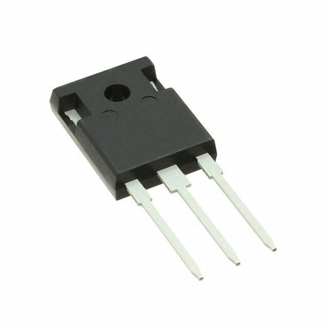
PG-TO247
• Periodic avalanche rated
• Extreme dv/dt rated
• Ultra low effective capacitances
• Improved transconductance
Type
SPW24N60C3
Package
PG-TO247
Ordering Code
Q67040-S4640
Marking
24N60C3
Maximum Ratings
Parameter
Symbol
Continuous drain current
ID
Value
Unit
A
TC = 25 °C
24.3
TC = 100 °C
15.4
Pulsed drain current, tp limited by Tjmax
I D puls
72.9
Avalanche energy, single pulse
EAS
780
mJ
I D = 10 A, VDD = 50 V
Avalanche energy, repetitive tAR limited by Tjmax1) EAR
1
I D = 24.3 A, VDD = 50 V
Avalanche current, repetitive tAR limited by Tjmax I AR
Gate source voltage static
VGS
24.3
A
±20
V
Gate source voltage AC (f >1Hz)
VGS
±30
Power dissipation, T C = 25°C
Ptot
240
W
Operating and storage temperature
T j , T stg
-55... +150
°C
Reverse diode dv/dt 4)
dv/dt
Rev. 2.5
Page 1
15
V/ns
2008-02-11
Please note the new package dimensions arccording to PCN 2009-134-A
�SPW24N60C3
Maximum Ratings
Parameter
Symbol
Drain Source voltage slope
dv/dt
Value
Unit
50
V/ns
Values
Unit
V DS = 480 , ID = 24.3 , Tj = 125 °C
Thermal Characteristics
Parameter
Symbol
min.
typ.
max.
Thermal resistance, junction - case
RthJC
-
-
0.52
Thermal resistance, junction - ambient, leaded
RthJA
-
-
62
Soldering temperature, wavesoldering
Tsold
-
-
260
K/W
°C
1.6 mm (0.063 in.) from case for 10s
Electrical Characteristics, at Tj=25°C unless otherwise specified
Parameter
Symbol
Conditions
Drain-source breakdown voltage V(BR)DSS VGS=0V, ID=0.25mA
Drain-Source avalanche
V(BR)DS VGS=0V, ID=24.3A
Values
Unit
min.
typ.
max.
600
-
-
-
700
-
2.1
3
3.9
V
breakdown voltage
Gate threshold voltage
VGS(th)
ID=1200µΑ, VGS=VDS
Zero gate voltage drain current
IDSS
VDS=600V, VGS=0V,
Gate-source leakage current
IGSS
Drain-source on-state resistance RDS(on)
Gate input resistance
Rev. 2.5
RG
µA
Tj=25°C,
-
0.1
1
Tj=150°C
-
-
100
VGS=20, VDS =0V
-
-
100
Ω
VGS=10V, ID=15.4A,
Tj=25°C
-
0.14
0.16
Tj=150°C
-
0.34
-
f=1MHz, open Drain
-
0.66
-
Page 2
nA
2008-02-11
Please note the new package dimensions arccording to PCN 2009-134-A
�SPW24N60C3
Electrical Characteristics , at Tj = 25 °C, unless otherwise specified
Parameter
Transconductance
Symbol
g fs
Conditions
V DS≥2*I D*RDS(on)max,
Values
Unit
min.
typ.
max.
-
21.5
-
S
pF
ID=15.4A
Input capacitance
Ciss
V GS=0V, V DS=25V,
-
3000
-
Output capacitance
Coss
f=1MHz
-
1000
-
Reverse transfer capacitance
Crss
-
60
-
-
141
-
-
224
-
-
13
-
Effective output capacitance, 2) Co(er)
V GS=0V,
energy related
V DS=0V to 480V
Effective output capacitance, 3) Co(tr)
pF
time related
Turn-on delay time
td(on)
V DD=380V, V GS=0/10V,
ns
ID=24.3A, R G=3.3
Rise time
tr
V DD=380V, V GS=0/10V,
-
21
-
Turn-off delay time
td(off)
ID=24.3A, R G=3.3Ω
-
140
-
Fall time
tf
-
14
-
-
12.7
-
-
45.8
-
-
104.9
135
-
5
-
Gate Charge Characteristics
Gate to source charge
Qgs
Gate to drain charge
Qgd
Gate charge total
Qg
VDD=480, ID=24.3A
VDD=480V, ID=24.3A,
nC
VGS=0 to 10V
Gate plateau voltage
V(plateau) VDD=480V, ID=24.3A
V
1Repetitve avalanche causes additional power losses that can be calculated as P =EAR*f.
AV
2C o(er) is a fixed capacitance that gives the same stored energy as Coss while VDS is rising from 0 to 80% V DSS.
3C
o(tr) is a fixed capacitance that gives the same charging time as Coss while V DS is rising from 0 to 80% V DSS.
4I
很抱歉,暂时无法提供与“SPW24N60C3FKSA1”相匹配的价格&库存,您可以联系我们找货
免费人工找货