32-Bit
Microcontroller
TC39x
32-Bit Single-Chip Microcontroller
BC/BD-Step
32-Bit Single-Chip Microcontroller
Data Sheet
V 1.2, 2021-03
Microcontrollers
OPEN MARKET VERSION
�Edition 2021-03
Published by
Infineon Technologies AG
81726 Munich, Germany
© 2021 Infineon Technologies AG
All Rights Reserved.
Legal Disclaimer
The information given in this document shall in no event be regarded as a guarantee of conditions or
characteristics. With respect to any examples or hints given herein, any typical values stated herein and/or any
information regarding the application of the device, Infineon Technologies hereby disclaims any and all warranties
and liabilities of any kind, including without limitation, warranties of non-infringement of intellectual property rights
of any third party.
Information
For further information on technology, delivery terms and conditions and prices, please contact the nearest
Infineon Technologies Office (www.infineon.com)
Warnings
Due to technical requirements, components may contain dangerous substances. For information on the types in
question, please contact the nearest Infineon Technologies Office.
Infineon Technologies components may be used in life-support devices or systems only with the express written
approval of Infineon Technologies, if a failure of such components can reasonably be expected to cause the failure
of that life-support device or system or to affect the safety or effectiveness of that device or system. Life support
devices or systems are intended to be implanted in the human body or to support and/or maintain and sustain
and/or protect human life. If they fail, it is reasonable to assume that the health of the user or other persons may
be endangered.
OPEN MARKET VERSION
�TC39x BC/BD-Step
Revision History
Page or Item
Subjects (major changes since previous revision)
V 0.4, 2015-05
Version 0.4 is the first version of this document
V 0.6, 2017-09
The history is documented in the last chapter
V 0.7, 2018-07
The history is documented in the last chapter
V 1.0, 2018-10
The history is documented in the last chapter
V 1.1, 2019-09
The history is documented in the last chapter
V 1.2, 2021-03
The history is documented in the last chapter
Data Sheet
3
OPEN MARKET VERSION
V 1.2, 2021-03
�TC39x BC/BD-Step
Trademarks of Infineon Technologies AG
AURIX™, C166™, CanPAK™, CIPOS™, CIPURSE™, EconoPACK™, CoolMOS™, CoolSET™,
CORECONTROL™, CROSSAVE™, DAVE™, DI-POL™, EasyPIM™, EconoBRIDGE™, EconoDUAL™,
EconoPIM™, EconoPACK™, EiceDRIVER™, eupec™, FCOS™, HITFET™, HybridPACK™, I²RF™,
ISOFACE™, IsoPACK™, MIPAQ™, ModSTACK™, my-d™, NovalithIC™, OptiMOS™, ORIGA™,
POWERCODE™; PRIMARION™, PrimePACK™, PrimeSTACK™, PRO-SIL™, PROFET™, RASIC™,
ReverSave™, SatRIC™, SIEGET™, SINDRION™, SIPMOS™, SmartLEWIS™, SOLID FLASH™, TEMPFET™,
thinQ!™, TRENCHSTOP™, TriCore™.
Other Trademarks
Advance Design System™ (ADS) of Agilent Technologies, AMBA™, ARM™, MULTI-ICE™, KEIL™,
PRIMECELL™, REALVIEW™, THUMB™, µVision™ of ARM Limited, UK. AUTOSAR™ is licensed by AUTOSAR
development partnership. Bluetooth™ of Bluetooth SIG Inc. CAT-iq™ of DECT Forum. COLOSSUS™,
FirstGPS™ of Trimble Navigation Ltd. EMV™ of EMVCo, LLC (Visa Holdings Inc.). EPCOS™ of Epcos AG.
FLEXGO™ of Microsoft Corporation. FlexRay™ is licensed by FlexRay Consortium. HYPERTERMINAL™ of
Hilgraeve Incorporated. IEC™ of Commission Electrotechnique Internationale. IrDA™ of Infrared Data
Association Corporation. ISO™ of INTERNATIONAL ORGANIZATION FOR STANDARDIZATION. MATLAB™ of
MathWorks, Inc. MAXIM™ of Maxim Integrated Products, Inc. MICROTEC™, NUCLEUS™ of Mentor Graphics
Corporation. MIPI™ of MIPI Alliance, Inc. MIPS™ of MIPS Technologies, Inc., USA. muRata™ of MURATA
MANUFACTURING CO., MICROWAVE OFFICE™ (MWO) of Applied Wave Research Inc., OmniVision™ of
OmniVision Technologies, Inc. Openwave™ Openwave Systems Inc. RED HAT™ Red Hat, Inc. RFMD™ RF
Micro Devices, Inc. SIRIUS™ of Sirius Satellite Radio Inc. SOLARIS™ of Sun Microsystems, Inc. SPANSION™
of Spansion LLC Ltd. Symbian™ of Symbian Software Limited. TAIYO YUDEN™ of Taiyo Yuden Co.
TEAKLITE™ of CEVA, Inc. TEKTRONIX™ of Tektronix Inc. TOKO™ of TOKO KABUSHIKI KAISHA TA. UNIX™
of X/Open Company Limited. VERILOG™, PALLADIUM™ of Cadence Design Systems, Inc. VLYNQ™ of Texas
Instruments Incorporated. VXWORKS™, WIND RIVER™ of WIND RIVER SYSTEMS, INC. ZETEX™ of Diodes
Zetex Limited.
Last Trademarks Update 2011-11-11
Data Sheet
4
OPEN MARKET VERSION
V 1.2, 2021-03
�TC39x BC/BD-Step
Table of Contents
1
Summary of Features . . . . . . . . . . . . . . . . . . . . . . . . . . . . . . . . . . . . . . . . . . . . . . . . . . . . . . . . . . . . . 7
2
2.1
2.2
2.3
2.4
2.5
Pin Definition and Functions: . . . . . . . . . . . . . . . . . . . . . . . . . . . . . . . . . . . . . . . . . . . . . . . . . . . . . 12
LFBGA-516 Package Variant Pin Configuration . . . . . . . . . . . . . . . . . . . . . . . . . . . . . . . . . . . . . . . . . 15
LFBGA-292 Package Variant Pin Configuration . . . . . . . . . . . . . . . . . . . . . . . . . . . . . . . . . . . . . . . . 173
LFBGA-292 ADAS Package Variant Pin Configuration . . . . . . . . . . . . . . . . . . . . . . . . . . . . . . . . . . 277
Sequence of Pads in Pad Frame . . . . . . . . . . . . . . . . . . . . . . . . . . . . . . . . . . . . . . . . . . . . . . . . . . . 376
Legend . . . . . . . . . . . . . . . . . . . . . . . . . . . . . . . . . . . . . . . . . . . . . . . . . . . . . . . . . . . . . . . . . . . . . . . 403
3
3.1
3.2
3.3
3.4
3.5
3.6
3.7
3.8
3.9
3.10
3.11
3.12
3.12.1
3.13
3.13.1
3.13.1.1
3.13.1.2
3.13.1.3
3.13.1.4
3.14
3.15
3.16
3.17
3.18
3.19
3.20
3.21
3.22
3.23
3.24
3.24.1
3.24.2
3.24.3
3.24.4
3.24.5
3.25
3.26
3.27
3.28
3.29
Electrical Specification . . . . . . . . . . . . . . . . . . . . . . . . . . . . . . . . . . . . . . . . . . . . . . . . . . . . . . . . .
Parameter Interpretation . . . . . . . . . . . . . . . . . . . . . . . . . . . . . . . . . . . . . . . . . . . . . . . . . . . . . . . . . .
Absolute Maximum Ratings . . . . . . . . . . . . . . . . . . . . . . . . . . . . . . . . . . . . . . . . . . . . . . . . . . . . . . .
Pin Reliability in Overload . . . . . . . . . . . . . . . . . . . . . . . . . . . . . . . . . . . . . . . . . . . . . . . . . . . . . . . . .
Operating Conditions . . . . . . . . . . . . . . . . . . . . . . . . . . . . . . . . . . . . . . . . . . . . . . . . . . . . . . . . . . . .
5 V / 3.3 V switchable Pads . . . . . . . . . . . . . . . . . . . . . . . . . . . . . . . . . . . . . . . . . . . . . . . . . . . . . . .
High performance LVDS Pads . . . . . . . . . . . . . . . . . . . . . . . . . . . . . . . . . . . . . . . . . . . . . . . . . . . . .
VADC Parameters . . . . . . . . . . . . . . . . . . . . . . . . . . . . . . . . . . . . . . . . . . . . . . . . . . . . . . . . . . . . . .
DSADC Parameters . . . . . . . . . . . . . . . . . . . . . . . . . . . . . . . . . . . . . . . . . . . . . . . . . . . . . . . . . . . . .
MHz Oscillator . . . . . . . . . . . . . . . . . . . . . . . . . . . . . . . . . . . . . . . . . . . . . . . . . . . . . . . . . . . . . . . . .
Back-up Clock . . . . . . . . . . . . . . . . . . . . . . . . . . . . . . . . . . . . . . . . . . . . . . . . . . . . . . . . . . . . . . . . . .
Temperature Sensor . . . . . . . . . . . . . . . . . . . . . . . . . . . . . . . . . . . . . . . . . . . . . . . . . . . . . . . . . . . . .
Power Supply Current . . . . . . . . . . . . . . . . . . . . . . . . . . . . . . . . . . . . . . . . . . . . . . . . . . . . . . . . . . . .
Calculating the 1.25 V Current Consumption . . . . . . . . . . . . . . . . . . . . . . . . . . . . . . . . . . . . . . . .
Power Supply Infrastructure and Supply Start-up . . . . . . . . . . . . . . . . . . . . . . . . . . . . . . . . . . . . . . .
Supply Ramp-up and Ramp-down Behavior . . . . . . . . . . . . . . . . . . . . . . . . . . . . . . . . . . . . . . . . .
Single Supply mode (a) . . . . . . . . . . . . . . . . . . . . . . . . . . . . . . . . . . . . . . . . . . . . . . . . . . . . . .
Single Supply mode (e) . . . . . . . . . . . . . . . . . . . . . . . . . . . . . . . . . . . . . . . . . . . . . . . . . . . . . .
External Supply mode (d) . . . . . . . . . . . . . . . . . . . . . . . . . . . . . . . . . . . . . . . . . . . . . . . . . . . . .
External Supply mode (h) . . . . . . . . . . . . . . . . . . . . . . . . . . . . . . . . . . . . . . . . . . . . . . . . . . . . .
Reset Timing . . . . . . . . . . . . . . . . . . . . . . . . . . . . . . . . . . . . . . . . . . . . . . . . . . . . . . . . . . . . . . . . . . .
EVR . . . . . . . . . . . . . . . . . . . . . . . . . . . . . . . . . . . . . . . . . . . . . . . . . . . . . . . . . . . . . . . . . . . . . . . . .
System Phase Locked Loop (SYS_PLL) . . . . . . . . . . . . . . . . . . . . . . . . . . . . . . . . . . . . . . . . . . . . .
Peripheral Phase Locked Loop (PER_PLL) . . . . . . . . . . . . . . . . . . . . . . . . . . . . . . . . . . . . . . . . . . .
AC Specifications . . . . . . . . . . . . . . . . . . . . . . . . . . . . . . . . . . . . . . . . . . . . . . . . . . . . . . . . . . . . . . .
JTAG Parameters . . . . . . . . . . . . . . . . . . . . . . . . . . . . . . . . . . . . . . . . . . . . . . . . . . . . . . . . . . . . . . .
DAP Parameters . . . . . . . . . . . . . . . . . . . . . . . . . . . . . . . . . . . . . . . . . . . . . . . . . . . . . . . . . . . . . . . .
ASCLIN SPI Master Timing . . . . . . . . . . . . . . . . . . . . . . . . . . . . . . . . . . . . . . . . . . . . . . . . . . . . . . .
QSPI Timings, Master and Slave Mode . . . . . . . . . . . . . . . . . . . . . . . . . . . . . . . . . . . . . . . . . . . . . .
MSC Timing 5 V Operation . . . . . . . . . . . . . . . . . . . . . . . . . . . . . . . . . . . . . . . . . . . . . . . . . . . . . . . .
Ethernet Interface (ETH) Characteristics . . . . . . . . . . . . . . . . . . . . . . . . . . . . . . . . . . . . . . . . . . . . .
ETH Measurement Reference Points . . . . . . . . . . . . . . . . . . . . . . . . . . . . . . . . . . . . . . . . . . . . . .
ETH Management Signal Parameters (ETH_MDC, ETH_MDIO) . . . . . . . . . . . . . . . . . . . . . . . . .
ETH MII Parameters . . . . . . . . . . . . . . . . . . . . . . . . . . . . . . . . . . . . . . . . . . . . . . . . . . . . . . . . . . .
ETH RMII Parameters . . . . . . . . . . . . . . . . . . . . . . . . . . . . . . . . . . . . . . . . . . . . . . . . . . . . . . . . . .
ETH RGMII Parameters . . . . . . . . . . . . . . . . . . . . . . . . . . . . . . . . . . . . . . . . . . . . . . . . . . . . . . . . .
E-Ray Parameters . . . . . . . . . . . . . . . . . . . . . . . . . . . . . . . . . . . . . . . . . . . . . . . . . . . . . . . . . . . . . .
HSCT Parameters . . . . . . . . . . . . . . . . . . . . . . . . . . . . . . . . . . . . . . . . . . . . . . . . . . . . . . . . . . . . . .
Inter-IC (I2C) Interface Timing . . . . . . . . . . . . . . . . . . . . . . . . . . . . . . . . . . . . . . . . . . . . . . . . . . . . .
SDMMC Interface Timing . . . . . . . . . . . . . . . . . . . . . . . . . . . . . . . . . . . . . . . . . . . . . . . . . . . . . . . . .
FSP Parameter . . . . . . . . . . . . . . . . . . . . . . . . . . . . . . . . . . . . . . . . . . . . . . . . . . . . . . . . . . . . . . . . .
Data Sheet
5
OPEN MARKET VERSION
405
405
406
407
410
413
432
435
439
442
444
445
446
452
453
454
454
456
458
460
462
465
473
474
475
476
478
480
482
486
488
488
489
490
491
492
493
495
497
500
501
V 1.2, 2021-03
�TC39x BC/BD-Step
3.30
3.31
3.31.1
3.31.2
3.31.3
3.31.4
3.32
3.33
3.34
3.34.1
Radar Interface Timing . . . . . . . . . . . . . . . . . . . . . . . . . . . . . . . . . . . . . . . . . . . . . . . . . . . . . . . . . . .
EBU Timings . . . . . . . . . . . . . . . . . . . . . . . . . . . . . . . . . . . . . . . . . . . . . . . . . . . . . . . . . . . . . . . . . . .
BFCLKO Output Clock Timing . . . . . . . . . . . . . . . . . . . . . . . . . . . . . . . . . . . . . . . . . . . . . . . . . . . .
EBU Asynchronous Timings . . . . . . . . . . . . . . . . . . . . . . . . . . . . . . . . . . . . . . . . . . . . . . . . . . . . .
EBU Burst Mode Access Timing . . . . . . . . . . . . . . . . . . . . . . . . . . . . . . . . . . . . . . . . . . . . . . . . . .
EBU Arbitration Signal Timing . . . . . . . . . . . . . . . . . . . . . . . . . . . . . . . . . . . . . . . . . . . . . . . . . . . .
Flash Target Parameters . . . . . . . . . . . . . . . . . . . . . . . . . . . . . . . . . . . . . . . . . . . . . . . . . . . . . . . . .
Quality Declarations . . . . . . . . . . . . . . . . . . . . . . . . . . . . . . . . . . . . . . . . . . . . . . . . . . . . . . . . . . . . .
Package Outline . . . . . . . . . . . . . . . . . . . . . . . . . . . . . . . . . . . . . . . . . . . . . . . . . . . . . . . . . . . . . . . .
Package Parameters . . . . . . . . . . . . . . . . . . . . . . . . . . . . . . . . . . . . . . . . . . . . . . . . . . . . . . . . . . .
502
503
503
503
507
509
510
515
517
518
4
4.1
4.2
4.3
4.4
4.5
History . . . . . . . . . . . . . . . . . . . . . . . . . . . . . . . . . . . . . . . . . . . . . . . . . . . . . . . . . . . . . . . . . . . . . . .
Changes from Version 0.4 to Version 0.6 . . . . . . . . . . . . . . . . . . . . . . . . . . . . . . . . . . . . . . . . . . . . .
Changes from Version 0.6 to Version 0.7 . . . . . . . . . . . . . . . . . . . . . . . . . . . . . . . . . . . . . . . . . . . . .
Changes from Version 0.7 to Version 1.0 . . . . . . . . . . . . . . . . . . . . . . . . . . . . . . . . . . . . . . . . . . . . .
Changes from Version 1.0 to Version 1.1 . . . . . . . . . . . . . . . . . . . . . . . . . . . . . . . . . . . . . . . . . . . .
Changes from Version 1.1 to Version 1.2 . . . . . . . . . . . . . . . . . . . . . . . . . . . . . . . . . . . . . . . . . . . .
519
519
529
535
541
542
Data Sheet
6
OPEN MARKET VERSION
V 1.2, 2021-03
�TC39x BC/BD-Step
Summary of Features
1
Summary of Features
The TC39x product family has the following features:
•
High Performance Microcontroller with six CPU cores
•
Six 32-bit super-scalar TriCore CPUs (TC1.6.2P), each having the following features:
–
Superior real-time performance
–
Strong bit handling
–
Fully integrated DSP capabilities
–
Multiply-accumulate unit able to sustain 2 MAC operations per cycle
–
Fully pipelined Floating point unit (FPU)
–
up to 300 MHz operation at full temperature range
–
up to 240/96 Kbyte Data Scratch-Pad RAM (DSPR)
–
up to 64 Kbyte Instruction Scratch-Pad RAM (PSPR)
–
up to 64 Kbyte Data RAM (DLMU)
–
32 Kbyte Instruction Cache (ICACHE)
–
16 Kbyte Data Cache (DCACHE)
•
Lockstepped shadow cores for four TC1.6.2P
•
Multiple on-chip memories
–
All embedded NVM and SRAM are ECC protected
–
up to 16 Mbyte Program Flash Memory (PFLASH)
–
up to 1 Mbyte Data Flash Memory (DFLASH 0) usable for EEPROM emulation
–
768 Kbyte Memory (LMU)
–
BootROM (BROM)
•
128-Channel DMA Controller with safe data transfer
•
Sophisticated interrupt system (ECC protected)
•
High performance on-chip bus structure
–
64-bit Cross Bar Interconnect (SRI) giving fast parallel access between bus masters, CPUs and memories
–
32-bit System Peripheral Bus (SPB) for on-chip peripheral and functional units
–
SRI to SPB bus bridges (SFI Bridge)
•
Optional Hardware Security Module (HSM) on some variants
•
Safety Management Unit (SMU) handling safety monitor alarms
•
Memory Test Unit with ECC, Memory Initialization and MBIST functions (MTU)
•
Hardware I/O Monitor (IOM) for checking of digital I/O
•
Versatile On-chip Peripheral Units
–
8 Asynchronous/Synchronous Serial Channels (ASCLIN) with hardware LIN support (V1.3, V2.0, V2.1 and
J2602) up to 50 MBaud
–
6 Queued SPI Interface Channels (QSPI) with master and slave capability up to 50 Mbit/s
–
2 High Speed Serial Link (HSSL) for serial inter-processor communication up to 320 Mbit/s
–
4 serial Micro Second Bus interfaces (MSC) for serial port expansion to external power devices
–
3 MCMCAN Modules with 4 CAN nodes for high efficiency data handling via FIFO buffering
–
25 Single Edge Nibble Transmission (SENT) channels for connection to sensors
–
2 FlexRayTM module with 2 channels (E-Ray) supporting V2.1
Data Sheet
7
OPEN MARKET VERSION
V 1.2, 2021-03
�TC39x BC/BD-Step
Summary of Features
•
•
–
One Generic Timer Module (GTM) providing a powerful set of digital signal filtering and timer functionality
to realize autonomous and complex Input/Output management
–
One Capture / Compare 6 module (Two kernels CCU60 and CCU61)
–
One General Purpose 12 Timer Unit (GPT120)
–
4 channel Peripheral Sensor Interface conforming to V1.3 (PSI5)
–
1 Peripheral Sensor Interface with Serial PHY (PSI5-S)
–
2 Inter-Integrated Circuit Bus Interface (I2C) conforming to V2.1
–
1 IEEE802.3 Ethernet MAC with RMII and MII interfaces (ETH)
–
1 external Bus interface (EBU)
Versatile Successive Approximation ADC (VADC)
–
Cluster of 20 independent ADC kernels
–
Input voltage range from 0 V to 5.5V (ADC supply)
Delta-Sigma ADC (DSADC)
–
14 channels
•
Digital programmable I/O ports
•
On-chip debug support for OCDS Level 1 (CPUs, DMA, On Chip Buses)
•
multi-core debugging, real time tracing, and calibration
•
four/five wire JTAG (IEEE 1149.1) or DAP (Device Access Port) interface
•
Power Management System and on-chip regulators
•
Clock Generation Unit with System PLL and Peripheral PLL
•
Embedded Voltage Regulator
•
Qualified for automotive application according to AEC-Q100 (only applicable after delivery release of the
corresponding sales codes)
•
ISO 26262 Safety Element out of Context for safety requirements up to ASIL D (only applicable for sales codes
listed within a released Safety Package Release Note from IFX)
Data Sheet
8
OPEN MARKET VERSION
V 1.2, 2021-03
�TC39x BC/BD-Step
Summary of Features
Ordering Information
The ordering code for Infineon microcontrollers provides an exact reference to the required product. This ordering
code identifies:
•
The derivative itself, i.e. its function set, the temperature range, and the supply voltage
•
The package and the type of delivery.
Table 1-1
Platform Feature Overview
Feature
CPUs
TC39x
Type
TC1.6.2
Cores / Checker Cores
6/4
Max. Freq.
300 MHz
Program
32 KB
Data
16 KB
PSPR
64 KB
DSPR
240 KB for CPU0,1/ 96 KB else
DLMU
64 KB
LMU
768 KB
DAM
128 KB
TCM
2 MB
XCM
2 MB
XTM
16 KB
Size
16 MB
Banks
5 x 3 MB, 1 x 1 MB
Data Flash
Size (single-ended)
1 MB (DF0) + 128 KB (DF1)
DMA
Channels
128
CONVCTRL
Modules
1
EVADC
Primary Groups/Channels
8 / 64
Secondary Groups/Channels
4 / 64
Fast Compare Channels
8
Channels
14
Cache per CPU
SRAM per CPU
SRAM global
Extension Memory
Program Flash
EDSADC
Data Sheet
9
OPEN MARKET VERSION
V 1.2, 2021-03
�TC39x BC/BD-Step
Summary of Features
Table 1-1
Platform Feature Overview (cont’d)
Feature
GTM
TC39x
Clusters
12 (5 @ 200MHz, 7 @ 100MHz)
TIM (8 ch)
8
TOM (16 ch)
6
ATOM (8 ch)
12
MCS (8 ch)
10
CMU / ICM
1/1
PSM
3
TBU channels
1)
4 (TBU0-3)
SPE
6
CMP / MON
1/1
BRC / DPLL
1/1
CDTM modules
7
DTM modules
24 (10 on TOM, 14 on ATOM)
GPT12
1
CCU6
1
STM
Modules
6
FlexRay
Modules
2
Channels
2x2
Modules
3
Nodes
3x4
of which support TT-CAN
1
Modules
6
HSCI Channels
2
ASCLIN
Modules
12
I2C
Interfaces
2
SENT
Channels
25
PSI5
Modules
4
PSI5-S
Modules
1
HSSL
Channels
2
MSC
Channels
4
EBU
External Bus
1
SDMMC
eMMC/SD Interface
1
Ethernet (10/100Mbit/1Gbit)
Modules
1
FCE
Modules
Safety Support
SMU
yes
IOM
yes
Timer
CAN
QSPI
SPU
Data Sheet
1
Modules
2
10
OPEN MARKET VERSION
V 1.2, 2021-03
�TC39x BC/BD-Step
Summary of Features
Table 1-1
Platform Feature Overview (cont’d)
Feature
TC39x
RIF
Modules
2
HSPDM
Modules
1
Security
HSM+
1
Debug
OCDS
yes
MCDS
yes
miniMCDS
no
miniMCDS TRAM
- KB
AGBT
yes
Standby RAM
2
SCR
yes
2)
Low Power Features
Packages
Type
LFBGA-516 / LFBGA-292
I/O
Type
5 V CMOS / 3.3 V CMOS / LVDS
Tambient
Range
−40 … +150°C
1) TBU3 has special purpose as angle clock.
2) The Aurora Gigabit Trace Module (AGBT) is a trace interface intended for development use only (not to be used in series
production). It is only available on the specific emulation devices with feature package E, T, and on ADAS devices with feature
package A, H of the TC39x, TC37xEXT, TC35x, TC33xEXT. AGBT I/O functions are only available for packages with 292
or more pins. For details on AGBT parameters see the “TC3xx Emulation Devices” Data Sheet.
Data Sheet
11
OPEN MARKET VERSION
V 1.2, 2021-03
�TC39x BC/BD-Step
Pin Definition and Functions:
2
Pin Definition and Functions:
The following figures are showing the TC39x Logic Symbols for the package variants:
•
LFBGA-516 (Figure 2-1)
•
LFBGA-292 (Figure 2-2)
•
LFBGA-292 ADAS feature set (Figure 2-3)
1
2
3
4
5
6
7
8
9
10
11
12
13
14
15
16
17
18
19
20
21
22
23
24
25
26
27
28
29
30
A
NC1
VEXT
NC
NC
P10.15
P10.13
P10.11
NC
NC
NC
P13.15
P13.13
P13.11
P13.9
P13.7
P13.5
NC
P14.15
P14.13
P14.11
NC
P15.15
P15.13
P15.11
NC
NC
NC
NC
VDDP3
VSS
A
B
NC
VSS
VEXT
NC
P10.14
NC
P10.10
P10.9
NC
NC
P13.14
P13.12
P13.10
NC
P13.6
P13.4
NC
P14.14
P14.12
NC
NC
P15.14
P15.12
P15.10
NC
NC
NC
VDDP3
VSS
VSS
B
C
NC
NC
NC
NC
C
D
NC
NC
NC
NC
D
E
NC
NC
NC
NC
E
F
P02.13
P02.12
NC1
VEXT
P10.7
P10.6
P10.2
P10.3
P10.0
P11.11
P11.9
P11.2
P13.3
P13.1
P14.8
P14.5
P14.1
P15.6
P15.4
P15.1
VDDP3
VSS
NC
NC
F
G
P02.15
P02.14
P02.0
VSS
VEXT
P10.8
P10.5
P10.4
P10.1
P11.12
P11.10
P11.3
P13.2
P13.0
P14.6
P14.3
P14.4
P14.0
P15.3
VDDP3
VSS
P15.0
NC
NC
G
H
NC
NC
P02.2
P02.1
P15.2
P20.14
VSS
VSS
H
J
NC
P01.0
P02.4
P02.3
P20.12
P20.13
VEBU
VEBU
J
K
VSS
VFLEX
K
P01.1
P01.2
P02.6
P02.5
P02.9
VSS
L
P01.8
P01.9
P02.8
P02.7
P02.11
P02.10
P11.15
P11.13
P11.14
P11.8
P11.5
P11.7
VDDSB
(VDD)
M
P01.11
P01.10
P00.0
P00.1
P01.4
P01.3
N
P01.13
P01.12
P00.2
P00.3
P01.6
P01.5
P
P01.15
P01.14
P00.4
P00.5
P00.6
P01.7
VSS
VSS
P00.10
AGBTC
LKP
(VSS)
VSS
AN42
AGBTC
LKN
(VSS)
VSS
VSS
R
NC
NC
P00.7
P00.9
P00.8
T
NC
P00.13
P00.11
P00.12
U
P00.15
P00.14
AN46
AN47
AN41
AN40
VSS
AN45
AN36 /
P40.6
AN38 /
P40.8
VDD
V
AN72
AN73
AN44
AN43
VDDSB
(VDD)
P11.6
P11.1
P11.4
P11.0
P14.10
P12.1
P14.9
P12.0
VSS
DAPE2
DAPE1
VSS
VSS
VSS
VSS
VSS
VSS
VSS
VSS
VSS
VSS
VSS
VSS
VSS
VSS
VSS
P14.7
P14.2
VSS
VSS
VSS
VSS
VSS
VSS
AGBTT
XN
(VSS)
AGBTT
XP
(VSS)
VSS
P15.5
P15.7
VDD
VDD
VSS
VSS
P20.9
P20.10
P20.11
P24.14
P24.15
ESR0
P20.6
P20.7
P20.8
P24.12
P24.13
L
ESR1
PORST
P20.1
P20.3
P24.10
P24.11
M
VDD
P21.7 /
TDO
P21.6 /
TDI
P20.2
P20.0
P24.8
P24.9
N
VSS
TCK
P21.1
P21.3
P21.5
P24.6
P24.7
P
VSS
DAPE0
TMS
P21.0
P21.2
P21.4
P24.4
P24.5
R
VSS
AGBTE
RR
(VSS)
P22.10
P22.11
TRST
VSS
P24.2
P24.3
T
VSS
VSS
P22.8
P22.9
XTAL2
XTAL1
P24.0
P24.1
U
VDD
P22.6
P22.7
VDD
VEXT
NC1
NC1
V
P22.4
P22.5
P22.1
P22.0
P25.6
NC
W
P23.7
P23.6
P22.3
P22.2
P25.14
P25.15
Y
VDD
VSS
VSS
P15.8
W
AN70 /
P41.2
AN71 /
P41.3
AN39 /
P40.9
AN37 /
P40.7
AN32 /
P40.4
AN34
Y
AN68 /
P41.0
AN69 /
P41.1
AN33 /
P40.5
AN35
AN31
AN23
AA
AN67 /
P40.15
AN66
VAREF
2
VAGND
2
AN30
AN22
AN15
AN12
AN6
AN4
AN0
VEVRS
B
P34.2
P34.4
P33.14
P32.5
VSS
P23.5
P23.3
P23.4
P25.12
P25.13
AA
AB
AN65
AN64 /
P41.8
AN29 /
P40.14
AN28 /
P40.13
NC1
AN17 /
P40.10
AN14
AN9
AN7
AN3
AN1
P34.1
P34.3
P34.5
P33.15
P32.6
P32.7
VSS
P23.1
P23.2
P25.10
P25.11
AB
AC
AN63 /
P41.7
AN62 /
P41.6
AN27 /
P40.3
AN26 /
P40.2
VEXT
P23.0
P25.8
P25.9
AC
AN61
AN25 /
P40.1
AN24 /
P40.0
P33.12
P32.1 /
VGATE
1P
P32.4
VSS
VEXT
P25.7
P25.5
AD
P33.13
P32.0 /
VGATE
1N
P32.2
P32.3
VSS
P25.4
P25.3
AE
AD
AN60
AN21
AN20
AN18 /
P40.11
VSSM
AN16
VDDM
AN13
VAREF
1
AN11
VAGND
1
AN8
AN10
AN2
AN5
P33.0
P33.1
P33.2
P33.3
P33.4
P33.5
VDD
P33.6
P33.7
P33.8
P33.9
P33.10
AE
AN59
AN58
AF
AN56
AN57
P25.2
P25.1
AF
AG
VAREF
3
VAGND
3
P26.0
P25.0
AG
AH
NC
NC
VEXT
VEBU
AH
AJ
NC
NC
VSS
VEXT
AJ
AK
AK
NC1
AN19 /
P40.12
VDD
P33.11
NC
AN54 /
P41.4
AN53
AN51
AN48
VSSM
VDDM
VSS
VEBU
P31.1
P31.3
P31.5
P31.7
P31.9
P31.11
P31.13
P31.15
VEBU
P30.1
P30.3
P30.5
P30.7
P30.9
P30.11
P30.13
P30.15
VEBU
VSS
5
6
7
8
9
10
11
12
13
14
15
16
17
18
19
20
21
22
23
24
25
26
27
28
29
30
NC1
NC
NC
AN55 /
P41.5
1
2
3
4
AN52
AN50
AN49
VSSM
VDDM
VSS
VEBU
P31.0
P31.2
P31.4
P31.6
P31.8
P31.10
P31.12
P31.14
NC
P30.0
P30.2
P30.4
P30.6
P30.8
P30.10
P30.12
P30.14
TC39xed - (top view)
Figure 2-1 Logic Symbol for the package variant LFBGA-516
Data Sheet
12
OPEN MARKET VERSION
V 1.2, 2021-03
�TC39x BC/BD-Step
Pin Definition and Functions:
1
2
3
4
5
6
7
8
9
10
11
12
13
14
15
16
17
18
19
20
A
NC1
VEXT
P10.7
P10.6
P10.2
P10.3
P10.0
P11.11
P11.9
P11.2
P13.3
P13.1
P14.8
P14.5
P14.1
P15.6
P15.4
P15.1
VDDP3
VSS
A
B
P02.0
VSS
VEXT
P10.8
P10.5
P10.4
P10.1
P11.12
P11.10
P11.3
P13.2
P13.0
P14.6
P14.3
P14.4
P14.0
P15.3
VDDP3
VSS
P15.0
B
C
P02.2
P02.1
P15.2
P20.14
C
D
P02.4
P02.3
VSS
VFLEX
P11.15
P11.14
P11.5
P11.6
P11.4
P14.10
P14.9
P14.7
P15.8
P15.7
VDD
VSS
P20.12
P20.13
D
E
P02.6
P02.5
P02.9
VSS
P11.13
P11.8
P11.7
P11.1
P11.0
P12.1
P12.0
P14.2
P15.5
VDD
VSS
P20.9
P20.10
P20.11
E
F
P02.8
P02.7
P02.11
P02.10
ESR0
P20.6
P20.7
P20.8
F
ESR1
PORST
P20.1
P20.3
G
VDD
P21.7 /
TDO
P21.6 /
TDI
P20.2
P20.0
H
VSS
TCK
P21.1
P21.3
P21.5
J
VSS
DAPE0
TMS
P21.0
P21.2
P21.4
K
VSS
AGBTE
RR
(VSS)
P22.10
P22.11
TRST
VSS
L
VSS
VSS
P22.8
P22.9
XTAL2
XTAL1
M
VDD
P22.6
P22.7
VDD
VEXT
N
P22.4
P22.5
P22.1
P22.0
P
P23.7
P23.6
P22.3
P22.2
R
G
P00.0
P00.1
P01.4
VDDSB
(VDD)
P01.3
VDDSB
(VDD)
H
P00.2
P00.3
P01.6
P01.5
J
P00.4
P00.5
P00.6
P01.7
VSS
VSS
P00.10
AGBTC
LKP
(VSS)
VSS
VSS
VSS
K
P00.7
P00.9
P00.8
L
P00.11
P00.12
AN43
AN42
AGBTC
LKN
(VSS)
M
AN46
AN47
AN41
AN40
VSS
N
AN44
AN45
AN36 /
P40.6
AN38 /
P40.8
VDD
VSS
DAPE2
DAPE1
VSS
VSS
VSS
VSS
VSS
VSS
VSS
VSS
VSS
VSS
VSS
VSS
VSS
VSS
VSS
VDD
VSS
VSS
VSS
VSS
VSS
VSS
VSS
VSS
AGBTT
XN
(VSS)
AGBTT
XP
(VSS)
VSS
P
AN39 /
P40.9
AN37 /
P40.7
AN32 /
P40.4
AN34
R
AN33 /
P40.5
AN35
AN31
AN23
T
VAREF
2
VAGND
2
AN30
AN22
AN15
AN12
AN6
AN4
AN0
VEVRS
B
P34.2
P34.4
P33.14
P32.5
VSS
P23.5
P23.3
P23.4
T
U
AN29 /
P40.14
AN28 /
P40.13
NC1
AN17 /
P40.10
AN14
AN9
AN7
AN3
AN1
P34.1
P34.3
P34.5
P33.15
P32.6
P32.7
VSS
P23.1
P23.2
U
V
AN27 /
P40.3
AN26 /
P40.2
VEXT
P23.0
V
P33.12
P32.1 /
VGATE
1P
P32.4
VSS
VEXT
W
P32.2
P32.3
VSS
Y
18
19
20
W
AN25 /
P40.1
Y
AN24 /
P40.0
AN19 /
P40.12
AN18 /
P40.11
AN16
VDD
AN13
AN11
AN8
AN2
NC1
AN21
AN20
VSSM
VDDM
VAREF
1
VAGND
1
AN10
AN5
1
2
3
4
5
6
7
8
9
P33.0
P33.2
P33.4
VDD
P33.6
P33.8
P33.10
P33.1
P33.3
P33.5
P33.7
P33.9
P33.11
P33.13
P32.0 /
VGATE
1N
10
11
12
13
14
15
16
17
TC39xed - (top view)
Figure 2-2
Data Sheet
Logic Symbol for the package variant LFBGA-292
13
OPEN MARKET VERSION
V 1.2, 2021-03
�TC39x BC/BD-Step
Pin Definition and Functions:
1
2
3
4
5
6
7
8
9
10
11
12
13
14
15
16
17
18
19
20
P51_9
P51_7
P51_5
P51_3
P51_1
P11.11
P11.9
P11.2
P14.8
P14.5
P14.1
P15.6
P15.4
P15.1
VDDP3
VSS
A
P51_8
P51_6
P51_4
P51_2
P51_0
P11.12
P11.10
P11.3
P14.6
P14.3
P14.4
P14.0
P15.3
VDDP3
VSS
P15.0
B
P15.2
P20.14
C
A
NC1
VEXT
NC
P51_1
1
B
NC
VSS
VEXT
P51_1
0
C
P50_1
P50_0
D
P50_3
P50_2
VSS
VFLEX
P11.15
P11.14
P11.5
P11.6
P11.4
P14.10
P14.9
P14.7
P15.8
P15.7
VDD
VSS
P20.12
P20.13
D
E
P50_5
P50_4
P10.0
VSS
P11.13
P11.8
P11.7
P11.1
P11.0
P12.1
P12.0
P14.2
P15.5
VDD
VSS
P20.9
P20.10
P20.11
E
F
P50_7
P50_6
P10.1
P10.2
ESR0
P20.6
P20.7
P20.8
F
G
P50_9
P50_8
P10.3
P10.4
ESR1
PORST
P20.1
P20.3
G
H
P50_1
1
P50_1
0
P10.5
P10.6
VDD
P21.7 /
TDO
P21.6 /
TDI
P20.2
P20.0
H
J
P02.0
P02.1
P10.8
P10.7
VSS
VSS
VSS
TCK
P21.1
P21.3
P21.5
J
P02.5
AGBTC
LKP
(VSS)
VSS
VSS
DAPE0
TMS
P21.0
P21.2
P21.4
K
VSS
VSS
AGBTE
RR
(VSS)
P22.10
P22.11
TRST
VSS
L
VSS
VSS
VSS
P22.8
P22.9
XTAL2
XTAL1
M
VDD
P22.6
P22.7
VDD
VEXT
N
P22.4
P22.5
P22.1
P22.0
P
P23.7
P23.6
P22.3
P22.2
R
K
P02.2
P02.3
P02.4
VDD
VDD
L
P02.6
P00.0
P02.7
P02.8
AGBTC
LKN
(VSS)
M
P00.2
P00.1
P00.3
P00.4
VSS
N
P00.8
P00.7
P00.6
P00.5
VDD
DAPE2
DAPE1
VSS
VSS
VSS
VSS
VSS
VSS
VSS
VSS
VSS
VSS
VSS
VSS
VSS
VSS
VSS
VDD
VSS
VSS
VSS
VSS
VSS
VSS
VSS
VSS
AGBTT
XN
(VSS)
AGBTT
XP
(VSS)
VSS
P
P00.10
P00.9
AN47
AN45
R
P00.11
P00.12
AN25 /
P40.1
AN23
T
VAREF
2
VAGND
2
AN24 /
P40.0
AN22
AN15
AN12
AN6
AN4
AN0
VEVRS
B
P34.2
P34.4
P33.14
P32.5
VSS
P23.5
P23.3
P23.4
T
U
AN44
AN46
NC1
AN17 /
P40.10
AN14
AN9
AN7
AN3
AN1
P34.1
P34.3
P34.5
P33.15
P32.6
P32.7
VSS
P23.1
P23.2
U
V
AN39 /
P40.9
AN37 /
P40.7
VEXT
P23.0
V
P33.12
P32.1 /
VGATE
1P
P32.4
VSS
VEXT
W
P32.2
P32.3
VSS
Y
18
19
20
W
AN36 /
P40.6
Y
AN38 /
P40.8
AN19 /
P40.12
AN18 /
P40.11
AN16
VDD
VSS
AN13
AN11
AN8
AN2
P33.0
P33.2
P33.4
VDD
P33.6
P33.8
P33.10
NC1
AN21
AN20
VSSM
VDDM
VAREF
1
VAGND
1
AN10
AN5
P33.1
P33.3
P33.5
P33.7
P33.9
P33.11
P33.13
P32.0 /
VGATE
1N
1
2
3
4
5
6
7
8
9
10
11
12
13
14
15
16
17
TC39xed_adas - (top view)
Figure 2-3
Data Sheet
Logic Symbol for the package variant LFBGA-292 ADAS
14
OPEN MARKET VERSION
V 1.2, 2021-03
�TC39x BC/BD-Step
Pin Definition and Functions: LFBGA-516 Package Variant Pin Configuration
2.1
LFBGA-516 Package Variant Pin Configuration
Table 2-1
Port 00 Functions
Ball
Symbol
Ctrl.
Buffer
Type
Function
M6
P00.0
I
FAST /
PU1 /
VEXT /
ES
General-purpose input
GTM_TIM5_IN4_10
GTM_TIM3_IN0_1
GTM_TIM2_IN0_1
Mux input channel 4 of TIM module 5
Mux input channel 0 of TIM module 3
Mux input channel 0 of TIM module 2
CCU61_CTRAPA
Trap input capture
CCU60_T12HRE
External timer start 12
MSC0_INJ0
Injection signal from port
GETH_MDIOA
MDIO Input
P00.0
O0
General-purpose output
GTM_TOUT9
O1
GTM muxed output
IOM_REF0_9
Reference input 0
ASCLIN3_ASCLK
O2
Shift clock output
ASCLIN3_ATX
O3
Transmit output
IOM_MON2_15
Monitor input 2
IOM_REF2_15
Reference input 2
—
O4
Reserved
CAN10_TXD
O5
CAN transmit output node 0
—
O6
Reserved
CCU60_COUT63
O7
T13 PWM channel 63
IOM_MON1_6
Monitor input 1
IOM_REF1_0
Reference input 1
GETH_MDIO
Data Sheet
O
MDIO Output
15
OPEN MARKET VERSION
V 1.2, 2021-03
�TC39x BC/BD-Step
Pin Definition and Functions: LFBGA-516 Package Variant Pin Configuration
Table 2-1
Port 00 Functions (cont’d)
Ball
Symbol
Ctrl.
Buffer
Type
Function
M7
P00.1
I
SLOW /
PU1 /
VEXT /
ES
General-purpose input
GTM_TIM5_IN5_11
GTM_TIM3_IN1_1
GTM_TIM2_IN1_1
Mux input channel 5 of TIM module 5
Mux input channel 1 of TIM module 3
Mux input channel 1 of TIM module 2
CCU60_CC60INB
T12 capture input 60
ASCLIN3_ARXE
Receive input
EDSADC_DSCIN5A
Modulator clock input, channel 5
CAN10_RXDA
CAN receive input node 0
PSI5_RX0A
RXD inputs (receive data) channel 0
CCU61_CC60INA
T12 capture input 60
SENT_SENT0B
Receive input channel 0
EDSADC_DSCIN7B
Modulator clock input, channel 7
EVADC_G9CH11
AI
EDSADC_EDS5NA
Analog input channel 11, group 9
Negative analog input channel 5, pin A
P00.1
O0
General-purpose output
GTM_TOUT10
O1
GTM muxed output
IOM_REF0_10
ASCLIN3_ATX
Reference input 0
O2
Transmit output
IOM_MON2_15
Monitor input 2
IOM_REF2_15
Reference input 2
—
O3
Reserved
EDSADC_DSCOUT5
O4
Modulator clock output
EDSADC_DSCOUT7
O5
Modulator clock output
SENT_SPC0
O6
Transmit output
CCU61_CC60
O7
T12 PWM channel 60
IOM_MON1_8
Monitor input 1
IOM_REF1_13
Reference input 1
Data Sheet
16
OPEN MARKET VERSION
V 1.2, 2021-03
�TC39x BC/BD-Step
Pin Definition and Functions: LFBGA-516 Package Variant Pin Configuration
Table 2-1
Port 00 Functions (cont’d)
Ball
Symbol
Ctrl.
Buffer
Type
Function
N6
P00.2
I
SLOW /
PU1 /
VEXT /
ES1
General-purpose input
GTM_TIM5_IN6_11
GTM_TIM3_IN1_2
GTM_TIM2_IN1_2
Mux input channel 6 of TIM module 5
Mux input channel 1 of TIM module 3
Mux input channel 1 of TIM module 2
EDSADC_DSDIN7B
Digital datastream input, channel 7
EDSADC_DSDIN5A
Digital datastream input, channel 5
SENT_SENT1B
Receive input channel 1
EVADC_G9CH10
AI
EDSADC_EDS5PA
Analog input channel 10, group 9
Positive analog input channel 5, pin A
P00.2
O0
General-purpose output
GTM_TOUT11
O1
GTM muxed output
IOM_REF0_11
Reference input 0
ASCLIN3_ASCLK
O2
Shift clock output
CAN21_TXD
O3
CAN transmit output node 1
PSI5_TX0
O4
TXD outputs (send data)
IOM_MON1_14
Monitor input 1
IOM_REF1_14
Reference input 1
CAN03_TXD
O5
CAN transmit output node 3
IOM_MON2_8
Monitor input 2
IOM_REF2_8
Reference input 2
QSPI3_SLSO4
O6
Master slave select output
CCU61_COUT60
O7
T12 PWM channel 60
IOM_MON1_11
Monitor input 1
IOM_REF1_10
Reference input 1
Data Sheet
17
OPEN MARKET VERSION
V 1.2, 2021-03
�TC39x BC/BD-Step
Pin Definition and Functions: LFBGA-516 Package Variant Pin Configuration
Table 2-1
Port 00 Functions (cont’d)
Ball
Symbol
Ctrl.
Buffer
Type
Function
N7
P00.3
I
SLOW /
PU1 /
VEXT /
ES1
General-purpose input
GTM_TIM5_IN7_10
GTM_TIM3_IN2_1
GTM_TIM2_IN2_1
Mux input channel 7 of TIM module 5
Mux input channel 2 of TIM module 3
Mux input channel 2 of TIM module 2
CCU60_CC61INB
T12 capture input 61
EDSADC_DSCIN3A
Modulator clock input, channel 3
EDSADC_ITR5F
Trigger/Gate input, channel 5
PSI5_RX1A
RXD inputs (receive data) channel 1
CAN03_RXDA
CAN receive input node 3
CAN21_RXDA
CAN receive input node 1
PSI5S_RXA
RX data input
SENT_SENT2B
Receive input channel 2
CCU61_CC61INA
T12 capture input 61
EVADC_G9CH9
AI
EDSADC_EDS5NB
Analog input channel 9, group 9
Negative analog input channel 5, pin B
P00.3
O0
General-purpose output
GTM_TOUT12
O1
GTM muxed output
IOM_REF0_12
Reference input 0
ASCLIN3_ASLSO
O2
Slave select signal output
—
O3
Reserved
EDSADC_DSCOUT3
O4
Modulator clock output
—
O5
Reserved
SENT_SPC2
O6
Transmit output
CCU61_CC61
O7
T12 PWM channel 61
IOM_MON1_9
Monitor input 1
IOM_REF1_12
Reference input 1
Data Sheet
18
OPEN MARKET VERSION
V 1.2, 2021-03
�TC39x BC/BD-Step
Pin Definition and Functions: LFBGA-516 Package Variant Pin Configuration
Table 2-1
Port 00 Functions (cont’d)
Ball
Symbol
Ctrl.
Buffer
Type
Function
P6
P00.4
I
SLOW /
PU1 /
VEXT /
ES1
General-purpose input
GTM_TIM6_IN4_1
GTM_TIM3_IN3_1
GTM_TIM2_IN3_1
Mux input channel 4 of TIM module 6
Mux input channel 3 of TIM module 3
Mux input channel 3 of TIM module 2
SCU_E_REQ2_2
ERU Channel 2 inputs 0 to 5 (0 is the LSB and 5 is the
MSB)
SENT_SENT3B
Receive input channel 3
EDSADC_DSDIN3A
Digital datastream input, channel 3
EDSADC_SGNA
Carrier sign signal input
ASCLIN10_ARXA
Receive input
GTM_DTMA5_0
CDTM5_DTM4
GTM_DTMT3_0
CDTM3_DTM0
EVADC_G9CH8
AI
EDSADC_EDS5PB
Analog input channel 8, group 9
Positive analog input channel 5, pin B
P00.4
O0
General-purpose output
GTM_TOUT13
O1
GTM muxed output
IOM_REF0_13
Reference input 0
PSI5S_TX
O2
TX data output
CAN11_TXD
O3
CAN transmit output node 1
PSI5_TX1
O4
TXD outputs (send data)
IOM_MON1_15
Monitor input 1
EVADC_FC4BFLOUT
O5
Boundary flag output, FC channel 4
SENT_SPC3
O6
Transmit output
CCU61_COUT61
O7
T12 PWM channel 61
IOM_MON1_12
Monitor input 1
IOM_REF1_9
Reference input 1
Data Sheet
19
OPEN MARKET VERSION
V 1.2, 2021-03
�TC39x BC/BD-Step
Pin Definition and Functions: LFBGA-516 Package Variant Pin Configuration
Table 2-1
Port 00 Functions (cont’d)
Ball
Symbol
Ctrl.
Buffer
Type
Function
P7
P00.5
I
SLOW /
PU1 /
VEXT /
ES1
General-purpose input
GTM_TIM3_IN4_1
GTM_TIM3_IN0_11
GTM_TIM2_IN4_1
Mux input channel 4 of TIM module 3
Mux input channel 0 of TIM module 3
Mux input channel 4 of TIM module 2
CCU60_CC62INB
T12 capture input 62
EDSADC_DSCIN2A
Modulator clock input, channel 2
PSI5_RX2A
RXD inputs (receive data) channel 2
CCU61_CC62INA
T12 capture input 62
SENT_SENT4B
Receive input channel 4
CAN11_RXDB
CAN receive input node 1
GTM_DTMT1_1
CDTM1_DTM0
GTM_DTMT4_2
CDTM4_DTM0
EVADC_G9CH7
AI
Analog input channel 7, group 9
P00.5
O0
General-purpose output
GTM_TOUT14
O1
GTM muxed output
IOM_REF0_14
Reference input 0
EDSADC_CGPWMN
O2
Negative carrier generator output
QSPI3_SLSO3
O3
Master slave select output
EDSADC_DSCOUT2
O4
Modulator clock output
EVADC_FC0BFLOUT
O5
Boundary flag output, FC channel 0
SENT_SPC4
O6
Transmit output
CCU61_CC62
O7
T12 PWM channel 62
IOM_MON1_10
Monitor input 1
IOM_REF1_11
Reference input 1
Data Sheet
20
OPEN MARKET VERSION
V 1.2, 2021-03
�TC39x BC/BD-Step
Pin Definition and Functions: LFBGA-516 Package Variant Pin Configuration
Table 2-1
Port 00 Functions (cont’d)
Ball
Symbol
Ctrl.
Buffer
Type
Function
P9
P00.6
I
SLOW /
PU1 /
VEXT /
ES1
General-purpose input
GTM_TIM3_IN5_1
GTM_TIM3_IN1_14
GTM_TIM2_IN5_1
Mux input channel 5 of TIM module 3
Mux input channel 1 of TIM module 3
Mux input channel 5 of TIM module 2
EDSADC_ITR4F
Trigger/Gate input, channel 4
EDSADC_DSDIN2A
Digital datastream input, channel 2
SENT_SENT5B
Receive input channel 5
ASCLIN5_ARXA
Receive input
GTM_DTMA6_0
CDTM6_DTM4
GTM_DTMT3_1
CDTM3_DTM0
EVADC_G9CH6
AI
Analog input channel 6, group 9
P00.6
O0
General-purpose output
GTM_TOUT15
O1
GTM muxed output
IOM_REF0_15
Reference input 0
EDSADC_CGPWMP
O2
Positive carrier generator output
EVADC_FC5BFLOUT
O3
Boundary flag output, FC channel 5
PSI5_TX2
O4
TXD outputs (send data)
IOM_REF1_15
Reference input 1
EVADC_EMUX10
O5
Control of external analog multiplexer interface 1
SENT_SPC5
O6
Transmit output
CCU61_COUT62
O7
T12 PWM channel 62
IOM_MON1_13
Monitor input 1
IOM_REF1_8
Reference input 1
Data Sheet
21
OPEN MARKET VERSION
V 1.2, 2021-03
�TC39x BC/BD-Step
Pin Definition and Functions: LFBGA-516 Package Variant Pin Configuration
Table 2-1
Port 00 Functions (cont’d)
Ball
Symbol
Ctrl.
Buffer
Type
Function
R6
P00.7
I
SLOW /
PU1 /
VEXT /
ES1
General-purpose input
GTM_TIM3_IN6_1
GTM_TIM3_IN2_11
GTM_TIM2_IN6_1
Mux input channel 6 of TIM module 3
Mux input channel 2 of TIM module 3
Mux input channel 6 of TIM module 2
CCU61_CC60INC
T12 capture input 60
SENT_SENT6B
Receive input channel 6
EDSADC_DSCIN4A
Modulator clock input, channel 4
GPT120_T2INA
Trigger/gate input of timer T2
CCU61_CCPOS0A
Hall capture input 0
CCU60_T12HRB
External timer start 12
GTM_DTMT0_2
CDTM0_DTM0
EVADC_G9CH5
AI
EDSADC_EDS4NA
Analog input channel 5, group 9
Negative analog input channel 4, pin A
P00.7
O0
General-purpose output
GTM_TOUT16
O1
GTM muxed output
ASCLIN5_ATX
O2
Transmit output
EVADC_FC2BFLOUT
O3
Boundary flag output, FC channel 2
EDSADC_DSCOUT4
O4
Modulator clock output
EVADC_EMUX11
O5
Control of external analog multiplexer interface 1
SENT_SPC6
O6
Transmit output
CCU61_CC60
O7
T12 PWM channel 60
IOM_MON1_8
Monitor input 1
IOM_REF1_13
Reference input 1
Data Sheet
22
OPEN MARKET VERSION
V 1.2, 2021-03
�TC39x BC/BD-Step
Pin Definition and Functions: LFBGA-516 Package Variant Pin Configuration
Table 2-1
Port 00 Functions (cont’d)
Ball
Symbol
Ctrl.
Buffer
Type
Function
R9
P00.8
I
SLOW /
PU1 /
VEXT /
ES1
General-purpose input
GTM_TIM3_IN7_1
GTM_TIM3_IN3_11
GTM_TIM2_IN7_1
Mux input channel 7 of TIM module 3
Mux input channel 3 of TIM module 3
Mux input channel 7 of TIM module 2
CCU61_CC61INC
T12 capture input 61
SENT_SENT7B
Receive input channel 7
EDSADC_DSDIN4A
Digital datastream input, channel 4
GPT120_T2EUDA
Count direction control input of timer T2
CCU61_CCPOS1A
Hall capture input 1
CCU60_T13HRB
External timer start 13
ASCLIN10_ARXB
Receive input
EVADC_G9CH4
AI
EDSADC_EDS4PA
Analog input channel 4, group 9
Positive analog input channel 4, pin A
P00.8
O0
General-purpose output
GTM_TOUT17
O1
GTM muxed output
QSPI3_SLSO6
O2
Master slave select output
ASCLIN10_ATX
O3
Transmit output
—
O4
Reserved
EVADC_EMUX12
O5
Control of external analog multiplexer interface 1
SENT_SPC7
O6
Transmit output
CCU61_CC61
O7
T12 PWM channel 61
IOM_MON1_9
Monitor input 1
IOM_REF1_12
Reference input 1
Data Sheet
23
OPEN MARKET VERSION
V 1.2, 2021-03
�TC39x BC/BD-Step
Pin Definition and Functions: LFBGA-516 Package Variant Pin Configuration
Table 2-1
Port 00 Functions (cont’d)
Ball
Symbol
Ctrl.
Buffer
Type
Function
R7
P00.9
I
SLOW /
PU1 /
VEXT /
ES1
General-purpose input
GTM_TIM4_IN0_7
GTM_TIM1_IN0_1
GTM_TIM0_IN0_1
Mux input channel 0 of TIM module 4
Mux input channel 0 of TIM module 1
Mux input channel 0 of TIM module 0
CCU61_CC62INC
T12 capture input 62
SENT_SENT8B
Receive input channel 8
CCU61_CCPOS2A
Hall capture input 2
EDSADC_DSCIN1A
Modulator clock input, channel 1
EDSADC_ITR3F
Trigger/Gate input, channel 3
GPT120_T4EUDA
Count direction control input of timer T4
CCU60_T13HRC
External timer start 13
CCU60_T12HRC
External timer start 12
EVADC_G9CH3
AI
EDSADC_EDS4NB
Analog input channel 3, group 9
Negative analog input channel 4, pin B
P00.9
O0
General-purpose output
GTM_TOUT18
O1
GTM muxed output
QSPI3_SLSO7
O2
Master slave select output
ASCLIN3_ARTS
O3
Ready to send output
EDSADC_DSCOUT1
O4
Modulator clock output
ASCLIN4_ATX
O5
Transmit output
SENT_SPC8
O6
Transmit output
CCU61_CC62
O7
T12 PWM channel 62
IOM_MON1_10
Monitor input 1
IOM_REF1_11
Reference input 1
Data Sheet
24
OPEN MARKET VERSION
V 1.2, 2021-03
�TC39x BC/BD-Step
Pin Definition and Functions: LFBGA-516 Package Variant Pin Configuration
Table 2-1
Port 00 Functions (cont’d)
Ball
Symbol
Ctrl.
Buffer
Type
Function
R10
P00.10
I
SLOW /
PU1 /
VEXT /
ES1
General-purpose input
GTM_TIM4_IN1_11
GTM_TIM1_IN1_1
GTM_TIM0_IN1_1
Mux input channel 1 of TIM module 1
Mux input channel 1 of TIM module 0
SENT_SENT9B
Receive input channel 9
EDSADC_DSDIN1A
Digital datastream input, channel 1
EVADC_G9CH2
AI
Analog input channel 2, group 9
EDSADC_EDS4PB
T6
Mux input channel 1 of TIM module 4
Positive analog input channel 4, pin B
P00.10
O0
General-purpose output
GTM_TOUT19
O1
GTM muxed output
ASCLIN4_ASCLK
O2
Shift clock output
—
O3
Reserved
—
O4
Reserved
—
O5
Reserved
SENT_SPC9
O6
Transmit output
CCU61_COUT63
O7
T13 PWM channel 63
IOM_MON1_7
Monitor input 1
IOM_REF1_7
Reference input 1
P00.11
I
GTM_TIM4_IN2_11
GTM_TIM1_IN2_1
GTM_TIM0_IN2_1
SLOW /
PU1 /
VEXT /
ES1
General-purpose input
Mux input channel 2 of TIM module 4
Mux input channel 2 of TIM module 1
Mux input channel 2 of TIM module 0
CCU60_CTRAPA
Trap input capture
EDSADC_DSCIN0A
Modulator clock input, channel 0
CCU61_T12HRE
External timer start 12
SENT_SENT10B
Receive input channel 10
EVADC_G9CH1
AI
EVADC_FC3CH0
Analog input channel 1, group 9
Analog input FC channel 3
P00.11
O0
General-purpose output
GTM_TOUT20
O1
GTM muxed output
ASCLIN4_ASLSO
O2
Slave select signal output
—
O3
Reserved
EDSADC_DSCOUT0
O4
Modulator clock output
—
O5
Reserved
—
O6
Reserved
—
O7
Reserved
Data Sheet
25
OPEN MARKET VERSION
V 1.2, 2021-03
�TC39x BC/BD-Step
Pin Definition and Functions: LFBGA-516 Package Variant Pin Configuration
Table 2-1
Port 00 Functions (cont’d)
Ball
Symbol
Ctrl.
Buffer
Type
Function
T7
P00.12
I
SLOW /
PU1 /
VEXT /
ES1
General-purpose input
GTM_TIM4_IN3_11
GTM_TIM1_IN3_1
GTM_TIM0_IN3_1
Mux input channel 3 of TIM module 1
Mux input channel 3 of TIM module 0
ASCLIN3_ACTSA
Clear to send input
EDSADC_DSDIN0A
Digital datastream input, channel 0
ASCLIN4_ARXA
Receive input
SENT_SENT11B
Receive input channel 11
EVADC_G9CH0
AI
Analog input channel 0, group 9
EVADC_FC2CH0
T2
Mux input channel 3 of TIM module 4
Analog input FC channel 2
P00.12
O0
General-purpose output
GTM_TOUT21
O1
GTM muxed output
—
O2
Reserved
—
O3
Reserved
—
O4
Reserved
—
O5
Reserved
—
O6
Reserved
CCU61_COUT63
O7
T13 PWM channel 63
IOM_MON1_7
Monitor input 1
IOM_REF1_7
Reference input 1
P00.13
I
GTM_TIM6_IN5_2
GTM_TIM5_IN0_1
GTM_TIM4_IN0_1
EDSADC_DSDIN6A
FAST /
PU1 /
VEXT /
ES
General-purpose input
Mux input channel 5 of TIM module 6
Mux input channel 0 of TIM module 5
Mux input channel 0 of TIM module 4
Digital datastream input, channel 6
P00.13
O0
General-purpose output
GTM_TOUT167
O1
GTM muxed output
—
O2
Reserved
—
O3
Reserved
CCU_EXTCLK1
O4
External Clock 1
—
O5
Reserved
—
O6
Reserved
—
O7
Reserved
Data Sheet
26
OPEN MARKET VERSION
V 1.2, 2021-03
�TC39x BC/BD-Step
Pin Definition and Functions: LFBGA-516 Package Variant Pin Configuration
Table 2-1
Port 00 Functions (cont’d)
Ball
Symbol
Ctrl.
Buffer
Type
Function
U2
P00.14
I
SLOW /
PU1 /
VEXT /
ES
General-purpose input
GTM_TIM6_IN6_2
GTM_TIM5_IN7_1
GTM_TIM4_IN7_1
EDSADC_DSCIN6A
U1
Mux input channel 6 of TIM module 6
Mux input channel 7 of TIM module 5
Mux input channel 7 of TIM module 4
Modulator clock input, channel 6
P00.14
O0
General-purpose output
GTM_TOUT166
O1
GTM muxed output
—
O2
Reserved
—
O3
Reserved
EDSADC_DSCOUT6
O4
Modulator clock output
—
O5
Reserved
—
O6
Reserved
—
O7
Reserved
P00.15
I
GTM_TIM6_IN7_2
GTM_TIM5_IN1_1
GTM_TIM4_IN1_1
EDSADC_ITR6F
FAST /
PU1 /
VEXT /
ES
General-purpose input
Mux input channel 7 of TIM module 6
Mux input channel 1 of TIM module 5
Mux input channel 1 of TIM module 4
Trigger/Gate input, channel 6
P00.15
O0
General-purpose output
GTM_TOUT168
O1
GTM muxed output
—
O2
Reserved
—
O3
Reserved
CCU_EXTCLK0
O4
External Clock 0
—
O5
Reserved
—
O6
Reserved
—
O7
Reserved
Data Sheet
27
OPEN MARKET VERSION
V 1.2, 2021-03
�TC39x BC/BD-Step
Pin Definition and Functions: LFBGA-516 Package Variant Pin Configuration
Table 2-2
Port 01 Functions
Ball
Symbol
Ctrl.
Buffer
Type
Function
J2
P01.0
I
SLOW /
PU1 /
VEXT /
ES
General-purpose input
GTM_TIM5_IN4_1
GTM_TIM4_IN4_1
GTM_TIM2_IN6_13
K1
Mux input channel 4 of TIM module 5
Mux input channel 4 of TIM module 4
Mux input channel 6 of TIM module 2
CAN21_RXDE
CAN receive input node 1
EDSADC_ITR6E
Trigger/Gate input, channel 6
CAN03_RXDF
CAN receive input node 3
ASCLIN6_ARXB
Receive input
P01.0
O0
General-purpose output
GTM_TOUT155
O1
GTM muxed output
—
O2
Reserved
—
O3
Reserved
—
O4
Reserved
—
O5
Reserved
—
O6
Reserved
—
O7
Reserved
P01.1
I
GTM_TIM5_IN1_2
GTM_TIM4_IN1_2
EDSADC_ITR8E
SLOW /
PU1 /
VEXT /
ES
General-purpose input
Mux input channel 1 of TIM module 5
Mux input channel 1 of TIM module 4
Trigger/Gate input, channel 8
ERAY1_RXDA1
Receive Channel A1
SENT_SENT15B
Receive input channel 15
P01.1
O0
General-purpose output
GTM_TOUT159
O1
GTM muxed output
—
O2
Reserved
—
O3
Reserved
ASCLIN6_ATX
O4
Transmit output
—
O5
Reserved
—
O6
Reserved
—
O7
Reserved
Data Sheet
28
OPEN MARKET VERSION
V 1.2, 2021-03
�TC39x BC/BD-Step
Pin Definition and Functions: LFBGA-516 Package Variant Pin Configuration
Table 2-2
Port 01 Functions (cont’d)
Ball
Symbol
Ctrl.
Buffer
Type
Function
K2
P01.2
I
SLOW /
PU1 /
VEXT /
ES
General-purpose input
GTM_TIM5_IN5_1
GTM_TIM4_IN5_1
EDSADC_DSCIN7A
M10
Mux input channel 5 of TIM module 5
Mux input channel 5 of TIM module 4
Modulator clock input, channel 7
P01.2
O0
General-purpose output
GTM_TOUT156
O1
GTM muxed output
—
O2
Reserved
CAN03_TXD
O3
CAN transmit output node 3
IOM_MON2_8
Monitor input 2
IOM_REF2_8
Reference input 2
—
O4
Reserved
CAN21_TXD
O5
CAN transmit output node 1
EDSADC_DSCOUT7
O6
Modulator clock output
—
O7
Reserved
P01.3
I
GTM_TIM4_IN5_2
GTM_TIM2_IN0_14
GTM_TIM0_IN5_8
SLOW /
PU1 /
VEXT /
ES
General-purpose input
Mux input channel 5 of TIM module 4
Mux input channel 0 of TIM module 2
Mux input channel 5 of TIM module 0
QSPI3_SLSIB
Slave select input
EDSADC_ITR7F
Trigger/Gate input, channel 7
EVADC_G9CH14
AI
Analog input channel 14, group 9
P01.3
O0
General-purpose output
GTM_TOUT111
O1
GTM muxed output
—
O2
Reserved
—
O3
Reserved
QSPI3_SLSO9
O4
Master slave select output
CAN01_TXD
O5
CAN transmit output node 1
IOM_MON2_6
Monitor input 2
IOM_REF2_6
Reference input 2
—
O6
Reserved
—
O7
Reserved
Data Sheet
29
OPEN MARKET VERSION
V 1.2, 2021-03
�TC39x BC/BD-Step
Pin Definition and Functions: LFBGA-516 Package Variant Pin Configuration
Table 2-2
Port 01 Functions (cont’d)
Ball
Symbol
Ctrl.
Buffer
Type
Function
M9
P01.4
I
SLOW /
PU1 /
VEXT /
ES
General-purpose input
GTM_TIM4_IN6_2
GTM_TIM2_IN1_14
GTM_TIM0_IN6_8
N10
Mux input channel 6 of TIM module 4
Mux input channel 1 of TIM module 2
Mux input channel 6 of TIM module 0
CAN01_RXDC
CAN receive input node 1
EDSADC_ITR7E
Trigger/Gate input, channel 7
EVADC_G9CH13
AI
Analog input channel 13, group 9
P01.4
O0
General-purpose output
GTM_TOUT112
O1
GTM muxed output
—
O2
Reserved
ASCLIN9_ASLSO
O3
Slave select signal output
QSPI3_SLSO10
O4
Master slave select output
—
O5
Reserved
—
O6
Reserved
—
O7
Reserved
P01.5
I
GTM_TIM5_IN3_2
GTM_TIM2_IN3_7
GTM_TIM2_IN2_7
SLOW /
PU1 /
VEXT /
ES
General-purpose input
Mux input channel 3 of TIM module 5
Mux input channel 3 of TIM module 2
Mux input channel 2 of TIM module 2
QSPI3_MRSTC
Master SPI data input
EDSADC_DSCIN8A
Modulator clock input, channel 8
ASCLIN9_ARXA
Receive input
EVADC_G9CH12
AI
Analog input channel 12, group 9
P01.5
O0
General-purpose output
GTM_TOUT113
O1
GTM muxed output
—
O2
Reserved
—
O3
Reserved
QSPI3_MRST
O4
Slave SPI data output
IOM_MON2_3
Monitor input 2
IOM_REF2_3
Reference input 2
—
O5
Reserved
EDSADC_DSCOUT8
O6
Modulator clock output
—
O7
Reserved
Data Sheet
30
OPEN MARKET VERSION
V 1.2, 2021-03
�TC39x BC/BD-Step
Pin Definition and Functions: LFBGA-516 Package Variant Pin Configuration
Table 2-2
Port 01 Functions (cont’d)
Ball
Symbol
Ctrl.
Buffer
Type
Function
N9
P01.6
I
FAST /
PU1 /
VEXT /
ES
General-purpose input
GTM_TIM5_IN6_2
GTM_TIM5_IN5_3
GTM_TIM2_IN5_7
P10
Mux input channel 6 of TIM module 5
Mux input channel 5 of TIM module 5
Mux input channel 5 of TIM module 2
QSPI3_MTSRC
Slave SPI data input
EDSADC_DSDIN8A
Digital datastream input, channel 8
P01.6
O0
General-purpose output
GTM_TOUT114
O1
GTM muxed output
—
O2
Reserved
ASCLIN9_ASCLK
O3
Shift clock output
QSPI3_MTSR
O4
Master SPI data output
—
O5
Reserved
—
O6
Reserved
—
O7
Reserved
P01.7
I
GTM_TIM5_IN7_2
GTM_TIM2_IN7_7
QSPI3_SCLKC
FAST /
PU1 /
VEXT /
ES
General-purpose input
Mux input channel 7 of TIM module 5
Mux input channel 7 of TIM module 2
Slave SPI clock inputs
EDSADC_ITR8F
Trigger/Gate input, channel 8
ASCLIN9_ARXB
Receive input
P01.7
O0
General-purpose output
GTM_TOUT115
O1
GTM muxed output
—
O2
Reserved
ASCLIN9_ATX
O3
Transmit output
QSPI3_SCLK
O4
Master SPI clock output
—
O5
Reserved
—
O6
Reserved
—
O7
Reserved
Data Sheet
31
OPEN MARKET VERSION
V 1.2, 2021-03
�TC39x BC/BD-Step
Pin Definition and Functions: LFBGA-516 Package Variant Pin Configuration
Table 2-2
Port 01 Functions (cont’d)
Ball
Symbol
Ctrl.
Buffer
Type
Function
L1
P01.8
I
SLOW /
PU1 /
VEXT /
ES
General-purpose input
GTM_TIM5_IN4_2
GTM_TIM5_IN0_10
GTM_TIM4_IN4_2
L2
Mux input channel 4 of TIM module 5
Mux input channel 0 of TIM module 5
Mux input channel 4 of TIM module 4
CAN00_RXDF
CAN receive input node 0
ERAY1_RXDB1
Receive Channel B1
EDSADC_DSDIN9A
Digital datastream input, channel 9
SENT_SENT17B
Receive input channel 17
ASCLIN0_ARXC
Receive input
CAN20_RXDE
CAN receive input node 0
ASCLIN7_ARXB
Receive input
P01.8
O0
General-purpose output
GTM_TOUT162
O1
GTM muxed output
—
O2
Reserved
—
O3
Reserved
—
O4
Reserved
—
O5
Reserved
—
O6
Reserved
EVADC_FC4BFLOUT
O7
Boundary flag output, FC channel 4
P01.9
I
GTM_TIM5_IN2_1
GTM_TIM5_IN1_11
GTM_TIM4_IN2_1
SLOW /
PU1 /
VEXT /
ES
General-purpose input
Mux input channel 2 of TIM module 5
Mux input channel 1 of TIM module 5
Mux input channel 2 of TIM module 4
EDSADC_DSCIN9A
Modulator clock input, channel 9
SENT_SENT16B
Receive input channel 16
P01.9
O0
General-purpose output
GTM_TOUT160
O1
GTM muxed output
ASCLIN7_ATX
O2
Transmit output
—
O3
Reserved
—
O4
Reserved
—
O5
Reserved
EDSADC_DSCOUT9
O6
Modulator clock output
EVADC_FC5BFLOUT
O7
Boundary flag output, FC channel 5
Data Sheet
32
OPEN MARKET VERSION
V 1.2, 2021-03
�TC39x BC/BD-Step
Pin Definition and Functions: LFBGA-516 Package Variant Pin Configuration
Table 2-2
Port 01 Functions (cont’d)
Ball
Symbol
Ctrl.
Buffer
Type
Function
M2
P01.10
I
SLOW /
PU1 /
VEXT /
ES
General-purpose input
GTM_TIM5_IN5_2
GTM_TIM5_IN2_9
GTM_TIM4_IN5_3
M1
Mux input channel 5 of TIM module 5
Mux input channel 2 of TIM module 5
Mux input channel 5 of TIM module 4
EDSADC_ITR9F
Trigger/Gate input, channel 9
SENT_SENT18B
Receive input channel 18
GTM_DTMT4_0
CDTM4_DTM0
GTM_DTMA6_1
CDTM6_DTM4
GTM_DTMT3_2
CDTM3_DTM0
P01.10
O0
General-purpose output
GTM_TOUT163
O1
GTM muxed output
ASCLIN7_ASCLK
O2
Shift clock output
—
O3
Reserved
—
O4
Reserved
—
O5
Reserved
—
O6
Reserved
EVADC_FC6BFLOUT
O7
Boundary flag output, FC channel 6
P01.11
I
GTM_TIM5_IN7_3
GTM_TIM5_IN3_11
GTM_TIM4_IN7_2
SLOW /
PU1 /
VEXT /
ES
General-purpose input
Mux input channel 7 of TIM module 5
Mux input channel 3 of TIM module 5
Mux input channel 7 of TIM module 4
EDSADC_ITR9E
Trigger/Gate input, channel 9
SENT_SENT19B
Receive input channel 19
GTM_DTMT4_1
CDTM4_DTM0
GTM_DTMA5_1
CDTM5_DTM4
GTM_DTMA6_2
CDTM6_DTM4
P01.11
O0
General-purpose output
GTM_TOUT165
O1
GTM muxed output
ASCLIN7_ASLSO
O2
Slave select signal output
—
O3
Reserved
—
O4
Reserved
—
O5
Reserved
—
O6
Reserved
EVADC_FC7BFLOUT
O7
Boundary flag output, FC channel 7
Data Sheet
33
OPEN MARKET VERSION
V 1.2, 2021-03
�TC39x BC/BD-Step
Pin Definition and Functions: LFBGA-516 Package Variant Pin Configuration
Table 2-2
Port 01 Functions (cont’d)
Ball
Symbol
Ctrl.
Buffer
Type
Function
N2
P01.12
I
FAST /
PU1 /
VEXT /
ES
General-purpose input
GTM_TIM6_IN0_3
GTM_TIM5_IN0_2
GTM_TIM4_IN0_2
N1
Mux input channel 0 of TIM module 6
Mux input channel 0 of TIM module 5
Mux input channel 0 of TIM module 4
EDSADC_DSDIN10A
Digital datastream input, channel 10
EDSADC_ITR10F
Trigger/Gate input, channel 10
P01.12
O0
General-purpose output
GTM_TOUT158
O1
GTM muxed output
ASCLIN7_ATX
O2
Transmit output
—
O3
Reserved
—
O4
Reserved
—
O5
Reserved
ERAY1_TXDA
O6
Transmit Channel A
—
O7
Reserved
P01.13
I
GTM_TIM6_IN1_3
GTM_TIM5_IN3_1
GTM_TIM4_IN3_1
FAST /
PU1 /
VEXT /
ES
General-purpose input
Mux input channel 1 of TIM module 6
Mux input channel 3 of TIM module 5
Mux input channel 3 of TIM module 4
EDSADC_DSCIN10A
Modulator clock input, channel 10
EDSADC_ITR10E
Trigger/Gate input, channel 10
P01.13
O0
General-purpose output
GTM_TOUT161
O1
GTM muxed output
ASCLIN0_ATX
O2
Transmit output
IOM_MON2_12
Monitor input 2
IOM_REF2_12
Reference input 2
—
O3
Reserved
CAN00_TXD
O4
CAN transmit output node 0
IOM_MON2_5
Monitor input 2
IOM_REF2_5
Reference input 2
CAN20_TXD
O5
CAN transmit output node 0
ERAY1_TXDB
O6
Transmit Channel B
EDSADC_DSCOUT10
O7
Modulator clock output
Data Sheet
34
OPEN MARKET VERSION
V 1.2, 2021-03
�TC39x BC/BD-Step
Pin Definition and Functions: LFBGA-516 Package Variant Pin Configuration
Table 2-2
Port 01 Functions (cont’d)
Ball
Symbol
Ctrl.
Buffer
Type
Function
P2
P01.14
I
FAST /
PU1 /
VEXT /
ES
General-purpose input
GTM_TIM6_IN2_3
GTM_TIM5_IN6_3
GTM_TIM4_IN6_3
P1
Mux input channel 2 of TIM module 6
Mux input channel 6 of TIM module 5
Mux input channel 6 of TIM module 4
EDSADC_DSDIN11A
Digital datastream input, channel 11
EDSADC_ITR11F
Trigger/Gate input, channel 11
P01.14
O0
General-purpose output
GTM_TOUT164
O1
GTM muxed output
—
O2
Reserved
—
O3
Reserved
—
O4
Reserved
—
O5
Reserved
ERAY1_TXENA
O6
Transmit Enable Channel A
—
O7
Reserved
P01.15
I
GTM_TIM6_IN3_3
GTM_TIM5_IN6_1
GTM_TIM4_IN6_1
SLOW /
PU1 /
VEXT /
ES
General-purpose input
Mux input channel 3 of TIM module 6
Mux input channel 6 of TIM module 5
Mux input channel 6 of TIM module 4
EDSADC_DSDIN7A
Digital datastream input, channel 7
EDSADC_DSCIN11A
Modulator clock input, channel 11
EDSADC_ITR11E
Trigger/Gate input, channel 11
P01.15
O0
General-purpose output
GTM_TOUT157
O1
GTM muxed output
—
O2
Reserved
—
O3
Reserved
—
O4
Reserved
—
O5
Reserved
—
O6
Reserved
EDSADC_DSCOUT11
O7
Modulator clock output
Data Sheet
35
OPEN MARKET VERSION
V 1.2, 2021-03
�TC39x BC/BD-Step
Pin Definition and Functions: LFBGA-516 Package Variant Pin Configuration
Table 2-3
Port 02 Functions
Ball
Symbol
Ctrl.
Buffer
Type
Function
G6
P02.0
I
FAST /
PU1 /
VEXT /
ES
General-purpose input
GTM_TIM1_IN0_2
GTM_TIM0_IN0_2
CCU61_CC60INB
Mux input channel 0 of TIM module 1
Mux input channel 0 of TIM module 0
T12 capture input 60
ASCLIN2_ARXG
Receive input
CCU60_CC60INA
T12 capture input 60
SCU_E_REQ3_2
ERU Channel 3 inputs 0 to 5 (0 is the LSB and 5 is the
MSB)
GTM_DTMA0_0
CDTM0_DTM4
P02.0
O0
General-purpose output
GTM_TOUT0
O1
GTM muxed output
IOM_REF0_0
ASCLIN2_ATX
Reference input 0
O2
Transmit output
IOM_MON2_14
Monitor input 2
IOM_REF2_14
Reference input 2
QSPI3_SLSO1
O3
Master slave select output
EDSADC_CGPWMN
O4
Negative carrier generator output
CAN00_TXD
O5
CAN transmit output node 0
IOM_MON2_5
Monitor input 2
IOM_REF2_5
Reference input 2
ERAY0_TXDA
O6
Transmit Channel A
CCU60_CC60
O7
T12 PWM channel 60
IOM_MON1_2
Monitor input 1
IOM_REF1_6
Reference input 1
Data Sheet
36
OPEN MARKET VERSION
V 1.2, 2021-03
�TC39x BC/BD-Step
Pin Definition and Functions: LFBGA-516 Package Variant Pin Configuration
Table 2-3
Port 02 Functions (cont’d)
Ball
Symbol
Ctrl.
Buffer
Type
Function
H7
P02.1
I
SLOW /
PU1 /
VEXT /
ES
General-purpose input
GTM_TIM1_IN1_2
GTM_TIM0_IN1_2
ERAY0_RXDA2
Mux input channel 1 of TIM module 1
Mux input channel 1 of TIM module 0
Receive Channel A2
ASCLIN2_ARXB
Receive input
CAN00_RXDA
CAN receive input node 0
SCU_E_REQ2_1
ERU Channel 2 inputs 0 to 5 (0 is the LSB and 5 is the
MSB)
P02.1
O0
General-purpose output
GTM_TOUT1
O1
GTM muxed output
IOM_REF0_1
Reference input 0
QSPI4_SLSO7
O2
Master slave select output
QSPI3_SLSO2
O3
Master slave select output
EDSADC_CGPWMP
O4
Positive carrier generator output
—
O5
Reserved
—
O6
Reserved
CCU60_COUT60
O7
T12 PWM channel 60
IOM_MON1_3
Monitor input 1
IOM_REF1_3
Reference input 1
Data Sheet
37
OPEN MARKET VERSION
V 1.2, 2021-03
�TC39x BC/BD-Step
Pin Definition and Functions: LFBGA-516 Package Variant Pin Configuration
Table 2-3
Port 02 Functions (cont’d)
Ball
Symbol
Ctrl.
Buffer
Type
Function
H6
P02.2
I
FAST /
PU1 /
VEXT /
ES
General-purpose input
GTM_TIM1_IN2_2
GTM_TIM0_IN2_2
CCU61_CC61INB
Mux input channel 2 of TIM module 1
Mux input channel 2 of TIM module 0
T12 capture input 61
CCU60_CC61INA
T12 capture input 61
SENT_SENT14B
Receive input channel 14
P02.2
O0
General-purpose output
GTM_TOUT2
O1
GTM muxed output
IOM_REF0_2
ASCLIN1_ATX
Reference input 0
O2
Transmit output
IOM_MON2_13
Monitor input 2
IOM_REF2_13
Reference input 2
QSPI3_SLSO3
O3
Master slave select output
PSI5_TX0
O4
TXD outputs (send data)
IOM_MON1_14
Monitor input 1
IOM_REF1_14
Reference input 1
CAN02_TXD
O5
CAN transmit output node 2
IOM_MON2_7
Monitor input 2
IOM_REF2_7
Reference input 2
ERAY0_TXDB
O6
Transmit Channel B
CCU60_CC61
O7
T12 PWM channel 61
IOM_MON1_1
Monitor input 1
IOM_REF1_5
Reference input 1
Data Sheet
38
OPEN MARKET VERSION
V 1.2, 2021-03
�TC39x BC/BD-Step
Pin Definition and Functions: LFBGA-516 Package Variant Pin Configuration
Table 2-3
Port 02 Functions (cont’d)
Ball
Symbol
Ctrl.
Buffer
Type
Function
J7
P02.3
I
SLOW /
PU1 /
VEXT /
ES
General-purpose input
GTM_TIM1_IN3_2
GTM_TIM0_IN3_2
EDSADC_DSCIN5B
Mux input channel 3 of TIM module 1
Mux input channel 3 of TIM module 0
Modulator clock input, channel 5
ERAY0_RXDB2
Receive Channel B2
CAN02_RXDB
CAN receive input node 2
ASCLIN1_ARXG
Receive input
MSC1_SDI1
Upstream assynchronous input signal
PSI5_RX0B
RXD inputs (receive data) channel 0
SENT_SENT13B
Receive input channel 13
P02.3
O0
General-purpose output
GTM_TOUT3
O1
GTM muxed output
IOM_REF0_3
Reference input 0
ASCLIN2_ASLSO
O2
Slave select signal output
QSPI3_SLSO4
O3
Master slave select output
EDSADC_DSCOUT5
O4
Modulator clock output
—
O5
Reserved
—
O6
Reserved
CCU60_COUT61
O7
T12 PWM channel 61
IOM_MON1_4
Monitor input 1
IOM_REF1_2
Reference input 1
Data Sheet
39
OPEN MARKET VERSION
V 1.2, 2021-03
�TC39x BC/BD-Step
Pin Definition and Functions: LFBGA-516 Package Variant Pin Configuration
Table 2-3
Port 02 Functions (cont’d)
Ball
Symbol
Ctrl.
Buffer
Type
Function
J6
P02.4
I
FAST /
PU1 /
VEXT /
ES
General-purpose input
GTM_TIM1_IN4_1
GTM_TIM0_IN4_1
CCU61_CC62INB
Mux input channel 4 of TIM module 1
Mux input channel 4 of TIM module 0
T12 capture input 62
EDSADC_DSDIN5B
Digital datastream input, channel 5
QSPI3_SLSIA
Slave select input
CCU60_CC62INA
T12 capture input 62
I2C0_SDAA
Serial Data Input 0
CAN11_RXDA
CAN receive input node 1
CAN0_ECTT1
External CAN time trigger input
SENT_SENT12B
Receive input channel 12
P02.4
O0
General-purpose output
GTM_TOUT4
O1
GTM muxed output
IOM_REF0_4
Reference input 0
ASCLIN2_ASCLK
O2
Shift clock output
QSPI3_SLSO0
O3
Master slave select output
PSI5S_CLK
O4
PSI5S CLK is a clock that can be used on a pin to drive
the external PHY.
I2C0_SDA
O5
Serial Data Output
ERAY0_TXENA
O6
Transmit Enable Channel A
CCU60_CC62
O7
T12 PWM channel 62
IOM_MON1_0
Monitor input 1
IOM_REF1_4
Reference input 1
Data Sheet
40
OPEN MARKET VERSION
V 1.2, 2021-03
�TC39x BC/BD-Step
Pin Definition and Functions: LFBGA-516 Package Variant Pin Configuration
Table 2-3
Port 02 Functions (cont’d)
Ball
Symbol
Ctrl.
Buffer
Type
Function
K7
P02.5
I
FAST /
PU1 /
VEXT /
ES
General-purpose input
GTM_TIM1_IN5_1
GTM_TIM0_IN5_1
EDSADC_DSCIN4B
Mux input channel 5 of TIM module 1
Mux input channel 5 of TIM module 0
Modulator clock input, channel 4
I2C0_SCLA
Serial Clock Input 0
PSI5_RX1B
RXD inputs (receive data) channel 1
PSI5S_RXB
RX data input
QSPI3_MRSTA
Master SPI data input
SENT_SENT3C
Receive input channel 3
CAN0_ECTT2
External CAN time trigger input
P02.5
O0
General-purpose output
GTM_TOUT5
O1
GTM muxed output
IOM_REF0_5
Reference input 0
CAN11_TXD
O2
CAN transmit output node 1
QSPI3_MRST
O3
Slave SPI data output
IOM_MON2_3
Monitor input 2
IOM_REF2_3
Reference input 2
EDSADC_DSCOUT4
O4
Modulator clock output
I2C0_SCL
O5
Serial Clock Output
ERAY0_TXENB
O6
Transmit Enable Channel B
CCU60_COUT62
O7
T12 PWM channel 62
IOM_MON1_5
Monitor input 1
IOM_REF1_1
Reference input 1
Data Sheet
41
OPEN MARKET VERSION
V 1.2, 2021-03
�TC39x BC/BD-Step
Pin Definition and Functions: LFBGA-516 Package Variant Pin Configuration
Table 2-3
Port 02 Functions (cont’d)
Ball
Symbol
Ctrl.
Buffer
Type
Function
K6
P02.6
I
FAST /
PU1 /
VEXT /
ES
General-purpose input
GTM_TIM3_IN0_10
GTM_TIM1_IN6_1
GTM_TIM0_IN6_1
Mux input channel 0 of TIM module 3
Mux input channel 6 of TIM module 1
Mux input channel 6 of TIM module 0
CCU60_CC60INC
T12 capture input 60
SENT_SENT2C
Receive input channel 2
EDSADC_DSDIN4B
Digital datastream input, channel 4
EDSADC_ITR5E
Trigger/Gate input, channel 5
GPT120_T3INA
Trigger/gate input of core timer T3
CCU60_CCPOS0A
Hall capture input 0
CCU61_T12HRB
External timer start 12
QSPI3_MTSRA
Slave SPI data input
RIF0_RAMP1B
External RAMP B input
P02.6
O0
General-purpose output
GTM_TOUT6
O1
GTM muxed output
IOM_REF0_6
Reference input 0
PSI5S_TX
O2
TX data output
QSPI3_MTSR
O3
Master SPI data output
PSI5_TX1
O4
TXD outputs (send data)
IOM_MON1_15
Monitor input 1
EVADC_EMUX00
O5
Control of external analog multiplexer interface 0
—
O6
Reserved
CCU60_CC60
O7
T12 PWM channel 60
IOM_MON1_2
Monitor input 1
IOM_REF1_6
Reference input 1
Data Sheet
42
OPEN MARKET VERSION
V 1.2, 2021-03
�TC39x BC/BD-Step
Pin Definition and Functions: LFBGA-516 Package Variant Pin Configuration
Table 2-3
Port 02 Functions (cont’d)
Ball
Symbol
Ctrl.
Buffer
Type
Function
L7
P02.7
I
FAST /
PU1 /
VEXT /
ES
General-purpose input
GTM_TIM3_IN1_10
GTM_TIM1_IN7_1
GTM_TIM0_IN7_1
Mux input channel 1 of TIM module 3
Mux input channel 7 of TIM module 1
Mux input channel 7 of TIM module 0
CCU60_CC61INC
T12 capture input 61
SENT_SENT1C
Receive input channel 1
EDSADC_DSCIN3B
Modulator clock input, channel 3
EDSADC_ITR4E
Trigger/Gate input, channel 4
GPT120_T3EUDA
Count direction control input of core timer T3
PSI5_RX2B
RXD inputs (receive data) channel 2
CCU60_CCPOS1A
Hall capture input 1
QSPI3_SCLKA
Slave SPI clock inputs
CCU61_T13HRB
External timer start 13
P02.7
O0
General-purpose output
GTM_TOUT7
O1
GTM muxed output
IOM_REF0_7
Reference input 0
—
O2
Reserved
QSPI3_SCLK
O3
Master SPI clock output
EDSADC_DSCOUT3
O4
Modulator clock output
EVADC_EMUX01
O5
Control of external analog multiplexer interface 0
SENT_SPC1
O6
Transmit output
CCU60_CC61
O7
T12 PWM channel 61
IOM_MON1_1
Monitor input 1
IOM_REF1_5
Reference input 1
Data Sheet
43
OPEN MARKET VERSION
V 1.2, 2021-03
�TC39x BC/BD-Step
Pin Definition and Functions: LFBGA-516 Package Variant Pin Configuration
Table 2-3
Port 02 Functions (cont’d)
Ball
Symbol
Ctrl.
Buffer
Type
Function
L6
P02.8
I
SLOW /
PU1 /
VEXT /
ES
General-purpose input
GTM_TIM3_IN2_10
GTM_TIM3_IN0_2
GTM_TIM2_IN0_2
Mux input channel 2 of TIM module 3
Mux input channel 0 of TIM module 3
Mux input channel 0 of TIM module 2
CCU60_CC62INC
T12 capture input 62
SENT_SENT0C
Receive input channel 0
CCU60_CCPOS2A
Hall capture input 2
EDSADC_DSDIN3B
Digital datastream input, channel 3
EDSADC_ITR3E
Trigger/Gate input, channel 3
GPT120_T4INA
Trigger/gate input of timer T4
CCU61_T12HRC
External timer start 12
CCU61_T13HRC
External timer start 13
GTM_DTMA0_1
CDTM0_DTM4
P02.8
O0
General-purpose output
GTM_TOUT8
O1
GTM muxed output
IOM_REF0_8
Reference input 0
QSPI3_SLSO5
O2
Master slave select output
ASCLIN8_ASCLK
O3
Shift clock output
PSI5_TX2
O4
TXD outputs (send data)
IOM_REF1_15
Reference input 1
EVADC_EMUX02
O5
Control of external analog multiplexer interface 0
GETH_MDC
O6
MDIO clock
CCU60_CC62
O7
T12 PWM channel 62
IOM_MON1_0
Monitor input 1
IOM_REF1_4
Reference input 1
Data Sheet
44
OPEN MARKET VERSION
V 1.2, 2021-03
�TC39x BC/BD-Step
Pin Definition and Functions: LFBGA-516 Package Variant Pin Configuration
Table 2-3
Port 02 Functions (cont’d)
Ball
Symbol
Ctrl.
Buffer
Type
Function
K9
P02.9
I
SLOW /
PU1 /
VEXT /
ES
General-purpose input
GTM_TIM4_IN2_2
GTM_TIM3_IN3_10
GTM_TIM0_IN2_10
L10
Mux input channel 2 of TIM module 4
Mux input channel 3 of TIM module 3
Mux input channel 2 of TIM module 0
SENT_SENT20B
Receive input channel 20
ASCLIN8_ARXA
Receive input
P02.9
O0
General-purpose output
GTM_TOUT116
O1
GTM muxed output
ASCLIN2_ATX
O2
Transmit output
IOM_MON2_14
Monitor input 2
IOM_REF2_14
Reference input 2
ASCLIN8_ATX
O3
Transmit output
—
O4
Reserved
CAN01_TXD
O5
CAN transmit output node 1
IOM_MON2_6
Monitor input 2
IOM_REF2_6
Reference input 2
—
O6
Reserved
—
O7
Reserved
P02.10
I
GTM_TIM4_IN3_2
GTM_TIM3_IN4_11
GTM_TIM0_IN3_10
SLOW /
PU1 /
VEXT /
ES
General-purpose input
Mux input channel 3 of TIM module 4
Mux input channel 4 of TIM module 3
Mux input channel 3 of TIM module 0
ASCLIN2_ARXC
Receive input
CAN01_RXDE
CAN receive input node 1
SENT_SENT21B
Receive input channel 21
ASCLIN8_ARXB
Receive input
P02.10
O0
General-purpose output
GTM_TOUT117
O1
GTM muxed output
—
O2
Reserved
—
O3
Reserved
—
O4
Reserved
—
O5
Reserved
—
O6
Reserved
—
O7
Reserved
Data Sheet
45
OPEN MARKET VERSION
V 1.2, 2021-03
�TC39x BC/BD-Step
Pin Definition and Functions: LFBGA-516 Package Variant Pin Configuration
Table 2-3
Port 02 Functions (cont’d)
Ball
Symbol
Ctrl.
Buffer
Type
Function
L9
P02.11
I
SLOW /
PU1 /
VEXT /
ES
General-purpose input
GTM_TIM4_IN4_3
GTM_TIM3_IN5_12
GTM_TIM0_IN7_7
SENT_SENT22B
F2
Mux input channel 4 of TIM module 4
Mux input channel 5 of TIM module 3
Mux input channel 7 of TIM module 0
Receive input channel 22
EVADC_G9CH15
AI
Analog input channel 15, group 9
P02.11
O0
General-purpose output
GTM_TOUT118
O1
GTM muxed output
—
O2
Reserved
ASCLIN8_ASLSO
O3
Slave select signal output
—
O4
Reserved
—
O5
Reserved
—
O6
Reserved
—
O7
Reserved
P02.12
I
GTM_TIM5_IN0_3
GTM_TIM4_IN0_3
GTM_TIM3_IN6_12
SLOW /
PU1 /
VEXT /
ES
General-purpose input
Mux input channel 0 of TIM module 5
Mux input channel 0 of TIM module 4
Mux input channel 6 of TIM module 3
EDSADC_DSDIN12A
Digital datastream input, channel 12
EDSADC_ITR12F
Trigger/Gate input, channel 12
SENT_SENT23B
Receive input channel 23
P02.12
O0
General-purpose output
GTM_TOUT151
O1
GTM muxed output
QSPI3_SLSO5
O2
Master slave select output
QSPI4_SLSO4
O3
Master slave select output
ASCLIN6_ASLSO
O4
Slave select signal output
—
O5
Reserved
—
O6
Reserved
—
O7
Reserved
Data Sheet
46
OPEN MARKET VERSION
V 1.2, 2021-03
�TC39x BC/BD-Step
Pin Definition and Functions: LFBGA-516 Package Variant Pin Configuration
Table 2-3
Port 02 Functions (cont’d)
Ball
Symbol
Ctrl.
Buffer
Type
Function
F1
P02.13
I
SLOW /
PU1 /
VEXT /
ES
General-purpose input
GTM_TIM5_IN2_2
GTM_TIM4_IN2_3
GTM_TIM3_IN7_11
G2
Mux input channel 2 of TIM module 5
Mux input channel 2 of TIM module 4
Mux input channel 7 of TIM module 3
EDSADC_DSCIN12A
Modulator clock input, channel 12
EDSADC_ITR12E
Trigger/Gate input, channel 12
SENT_SENT24B
Receive input channel 24
P02.13
O0
General-purpose output
GTM_TOUT153
O1
GTM muxed output
QSPI3_SLSO7
O2
Master slave select output
QSPI4_SLSO6
O3
Master slave select output
CAN00_TXD
O4
CAN transmit output node 0
IOM_MON2_5
Monitor input 2
IOM_REF2_5
Reference input 2
CAN20_TXD
O5
CAN transmit output node 0
—
O6
Reserved
EDSADC_DSCOUT12
O7
Modulator clock output
P02.14
I
GTM_TIM5_IN3_3
GTM_TIM4_IN3_3
GTM_TIM2_IN4_14
SLOW /
PU1 /
VEXT /
ES
General-purpose input
Mux input channel 3 of TIM module 5
Mux input channel 3 of TIM module 4
Mux input channel 4 of TIM module 2
CAN20_RXDD
CAN receive input node 0
CAN00_RXDH
CAN receive input node 0
EDSADC_DSDIN13A
Digital datastream input, channel 13
EDSADC_ITR13F
Trigger/Gate input, channel 13
P02.14
O0
General-purpose output
GTM_TOUT154
O1
GTM muxed output
ASCLIN6_ASCLK
O2
Shift clock output
—
O3
Reserved
—
O4
Reserved
—
O5
Reserved
—
O6
Reserved
—
O7
Reserved
Data Sheet
47
OPEN MARKET VERSION
V 1.2, 2021-03
�TC39x BC/BD-Step
Pin Definition and Functions: LFBGA-516 Package Variant Pin Configuration
Table 2-3
Port 02 Functions (cont’d)
Ball
Symbol
Ctrl.
Buffer
Type
Function
G1
P02.15
I
FAST /
PU1 /
VEXT /
ES
General-purpose input
GTM_TIM5_IN1_3
GTM_TIM4_IN1_3
GTM_TIM2_IN5_14
Mux input channel 1 of TIM module 5
Mux input channel 1 of TIM module 4
Mux input channel 5 of TIM module 2
EDSADC_DSCIN13A
Modulator clock input, channel 13
EDSADC_ITR13E
Trigger/Gate input, channel 13
P02.15
O0
General-purpose output
GTM_TOUT152
O1
GTM muxed output
QSPI3_SLSO6
O2
Master slave select output
QSPI4_SLSO5
O3
Master slave select output
ASCLIN6_ATX
O4
Transmit output
—
O5
Reserved
ERAY1_TXENB
O6
Transmit Enable Channel B
EDSADC_DSCOUT13
O7
Modulator clock output
Table 2-4
Port 10 Functions
Ball
Symbol
Ctrl.
Buffer
Type
Function
F12
P10.0
I
SLOW /
PU1 /
VEXT /
ES
General-purpose input
GTM_TIM4_IN0_12
GTM_TIM1_IN4_2
GTM_TIM0_IN4_2
Mux input channel 0 of TIM module 4
Mux input channel 4 of TIM module 1
Mux input channel 4 of TIM module 0
GPT120_T6EUDB
Count direction control input of core timer T6
ASCLIN11_ARXA
Receive input
GETH_RXERC
Receive Error MII
GTM_DTMA5_2
CDTM5_DTM4
P10.0
O0
General-purpose output
GTM_TOUT102
O1
GTM muxed output
ASCLIN11_ATX
O2
Transmit output
QSPI1_SLSO10
O3
Master slave select output
—
O4
Reserved
EVADC_FC6BFLOUT
O5
Boundary flag output, FC channel 6
—
O6
Reserved
—
O7
Reserved
Data Sheet
48
OPEN MARKET VERSION
V 1.2, 2021-03
�TC39x BC/BD-Step
Pin Definition and Functions: LFBGA-516 Package Variant Pin Configuration
Table 2-4
Port 10 Functions (cont’d)
Ball
Symbol
Ctrl.
Buffer
Type
Function
G12
P10.1
I
FAST /
PU1 /
VEXT /
ES
General-purpose input
GTM_TIM4_IN4_12
GTM_TIM1_IN1_3
GTM_TIM0_IN1_3
F10
Mux input channel 4 of TIM module 4
Mux input channel 1 of TIM module 1
Mux input channel 1 of TIM module 0
GPT120_T5EUDB
Count direction control input of timer T5
QSPI1_MRSTA
Master SPI data input
GTM_DTMT0_1
CDTM0_DTM0
P10.1
O0
General-purpose output
GTM_TOUT103
O1
GTM muxed output
QSPI1_MTSR
O2
Master SPI data output
QSPI1_MRST
O3
Slave SPI data output
IOM_MON2_1
Monitor input 2
IOM_REF2_1
Reference input 2
MSC0_EN1
O4
Chip Select
EVADC_FC1BFLOUT
O5
Boundary flag output, FC channel 1
—
O6
Reserved
—
O7
Reserved
P10.2
I
GTM_TIM4_IN5_12
GTM_TIM1_IN2_3
GTM_TIM0_IN2_3
FAST /
PU1 /
VEXT /
ES
General-purpose input
Mux input channel 5 of TIM module 4
Mux input channel 2 of TIM module 1
Mux input channel 2 of TIM module 0
CAN02_RXDE
CAN receive input node 2
MSC0_SDI1
Upstream assynchronous input signal
QSPI1_SCLKA
Slave SPI clock inputs
GPT120_T6INB
Trigger/gate input of core timer T6
SCU_E_REQ2_0
ERU Channel 2 inputs 0 to 5 (0 is the LSB and 5 is the
MSB)
GTM_DTMT2_2
CDTM2_DTM0
P10.2
O0
General-purpose output
GTM_TOUT104
O1
GTM muxed output
IOM_MON2_9
Monitor input 2
—
O2
Reserved
QSPI1_SCLK
O3
Master SPI clock output
MSC0_EN0
O4
Chip Select
EVADC_FC3BFLOUT
O5
Boundary flag output, FC channel 3
—
O6
Reserved
—
O7
Reserved
Data Sheet
49
OPEN MARKET VERSION
V 1.2, 2021-03
�TC39x BC/BD-Step
Pin Definition and Functions: LFBGA-516 Package Variant Pin Configuration
Table 2-4
Port 10 Functions (cont’d)
Ball
Symbol
Ctrl.
Buffer
Type
Function
F11
P10.3
I
FAST /
PU1 /
VEXT /
ES
General-purpose input
GTM_TIM4_IN6_10
GTM_TIM1_IN3_3
GTM_TIM0_IN3_3
Mux input channel 3 of TIM module 1
Mux input channel 3 of TIM module 0
QSPI1_MTSRA
Slave SPI data input
SCU_E_REQ3_0
ERU Channel 3 inputs 0 to 5 (0 is the LSB and 5 is the
MSB)
GPT120_T5INB
Trigger/gate input of timer T5
P10.3
O0
General-purpose output
GTM_TOUT105
O1
GTM muxed output
IOM_MON2_10
G11
Mux input channel 6 of TIM module 4
Monitor input 2
—
O2
Reserved
QSPI1_MTSR
O3
Master SPI data output
MSC0_EN0
O4
Chip Select
—
O5
Reserved
CAN02_TXD
O6
CAN transmit output node 2
IOM_MON2_7
Monitor input 2
IOM_REF2_7
Reference input 2
—
O7
P10.4
I
GTM_TIM4_IN7_3
GTM_TIM1_IN6_2
GTM_TIM0_IN6_2
Reserved
FAST /
PU1 /
VEXT /
ES
General-purpose input
Mux input channel 7 of TIM module 4
Mux input channel 6 of TIM module 1
Mux input channel 6 of TIM module 0
QSPI1_MTSRC
Slave SPI data input
CCU60_CCPOS0C
Hall capture input 0
GPT120_T3INB
Trigger/gate input of core timer T3
ASCLIN11_ARXB
Receive input
P10.4
O0
General-purpose output
GTM_TOUT106
O1
GTM muxed output
IOM_MON2_11
Monitor input 2
—
O2
Reserved
QSPI1_SLSO8
O3
Master slave select output
QSPI1_MTSR
O4
Master SPI data output
MSC0_EN0
O5
Chip Select
—
O6
Reserved
—
O7
Reserved
Data Sheet
50
OPEN MARKET VERSION
V 1.2, 2021-03
�TC39x BC/BD-Step
Pin Definition and Functions: LFBGA-516 Package Variant Pin Configuration
Table 2-4
Port 10 Functions (cont’d)
Ball
Symbol
Ctrl.
Buffer
Type
Function
G10
P10.5
I
SLOW /
PU2 /
VEXT /
ES
General-purpose input
GTM_TIM4_IN3_13
GTM_TIM1_IN2_4
GTM_TIM0_IN2_4
Mux input channel 3 of TIM module 4
Mux input channel 2 of TIM module 1
Mux input channel 2 of TIM module 0
PMS_HWCFG4IN
HWCFG4 pin input
CAN20_RXDA
CAN receive input node 0
MSC0_INJ1
Injection signal from port
P10.5
O0
General-purpose output
GTM_TOUT107
O1
GTM muxed output
IOM_REF2_9
ASCLIN2_ATX
Reference input 2
O2
Transmit output
IOM_MON2_14
Monitor input 2
IOM_REF2_14
Reference input 2
QSPI3_SLSO8
O3
Master slave select output
QSPI1_SLSO9
O4
Master slave select output
GPT120_T6OUT
O5
External output for overflow/underflow detection of
core timer T6
ASCLIN2_ASLSO
O6
Slave select signal output
PSI5_TX3
O7
TXD outputs (send data)
Data Sheet
51
OPEN MARKET VERSION
V 1.2, 2021-03
�TC39x BC/BD-Step
Pin Definition and Functions: LFBGA-516 Package Variant Pin Configuration
Table 2-4
Port 10 Functions (cont’d)
Ball
Symbol
Ctrl.
Buffer
Type
Function
F9
P10.6
I
SLOW /
PU2 /
VEXT /
ES
General-purpose input
GTM_TIM4_IN2_13
GTM_TIM1_IN3_4
GTM_TIM0_IN3_4
Mux input channel 2 of TIM module 4
Mux input channel 3 of TIM module 1
Mux input channel 3 of TIM module 0
PSI5_RX3C
RXD inputs (receive data) channel 3
ASCLIN2_ARXD
Receive input
QSPI3_MTSRB
Slave SPI data input
PMS_HWCFG5IN
HWCFG5 pin input
P10.6
O0
General-purpose output
GTM_TOUT108
O1
GTM muxed output
IOM_REF2_10
Reference input 2
ASCLIN2_ASCLK
O2
Shift clock output
QSPI3_MTSR
O3
Master SPI data output
GPT120_T3OUT
O4
External output for overflow/underflow detection of
core timer T3
CAN20_TXD
O5
CAN transmit output node 0
QSPI1_MRST
O6
Slave SPI data output
IOM_MON2_1
Monitor input 2
IOM_REF2_1
Reference input 2
EVADC_FC7BFLOUT
Data Sheet
O7
Boundary flag output, FC channel 7
52
OPEN MARKET VERSION
V 1.2, 2021-03
�TC39x BC/BD-Step
Pin Definition and Functions: LFBGA-516 Package Variant Pin Configuration
Table 2-4
Port 10 Functions (cont’d)
Ball
Symbol
Ctrl.
Buffer
Type
Function
F8
P10.7
I
SLOW /
PU1 /
VEXT /
ES
General-purpose input
GTM_TIM1_IN0_3
GTM_TIM0_IN0_3
GPT120_T3EUDB
Mux input channel 0 of TIM module 1
Mux input channel 0 of TIM module 0
Count direction control input of core timer T3
ASCLIN2_ACTSA
Clear to send input
QSPI3_MRSTB
Master SPI data input
SCU_E_REQ0_2
ERU Channel 0 inputs 0 to 5 (0 is the LSB and 5 is the
MSB)
CCU60_CCPOS1C
Hall capture input 1
P10.7
O0
General-purpose output
GTM_TOUT109
O1
GTM muxed output
IOM_REF2_11
Reference input 2
—
O2
Reserved
QSPI3_MRST
O3
Slave SPI data output
IOM_MON2_3
Monitor input 2
IOM_REF2_3
Reference input 2
—
O4
Reserved
CAN20_TXD
O5
CAN transmit output node 0
CAN12_TXD
O6
CAN transmit output node 2
—
O7
Reserved
Data Sheet
53
OPEN MARKET VERSION
V 1.2, 2021-03
�TC39x BC/BD-Step
Pin Definition and Functions: LFBGA-516 Package Variant Pin Configuration
Table 2-4
Port 10 Functions (cont’d)
Ball
Symbol
Ctrl.
Buffer
Type
Function
G9
P10.8
I
SLOW /
PU1 /
VEXT /
ES
General-purpose input
GTM_TIM4_IN0_13
GTM_TIM1_IN5_2
GTM_TIM0_IN5_2
B8
Mux input channel 0 of TIM module 4
Mux input channel 5 of TIM module 1
Mux input channel 5 of TIM module 0
CAN12_RXDB
CAN receive input node 2
GPT120_T4INB
Trigger/gate input of timer T4
QSPI3_SCLKB
Slave SPI clock inputs
SCU_E_REQ1_2
ERU Channel 1 inputs 0 to 5 (0 is the LSB and 5 is the
MSB)
CCU60_CCPOS2C
Hall capture input 2
CAN20_RXDB
CAN receive input node 0
RIF1_RAMP1B
External RAMP B input
P10.8
O0
General-purpose output
GTM_TOUT110
O1
GTM muxed output
ASCLIN2_ARTS
O2
Ready to send output
QSPI3_SCLK
O3
Master SPI clock output
—
O4
Reserved
—
O5
Reserved
—
O6
Reserved
—
O7
Reserved
P10.9
I
GTM_TIM6_IN0_5
GTM_TIM4_IN1_4
GTM_TIM0_IN1_10
SLOW /
PU1 /
VEXT /
ES
General-purpose input
Mux input channel 0 of TIM module 6
Mux input channel 1 of TIM module 4
Mux input channel 1 of TIM module 0
SENT_SENT15C
Receive input channel 15
ASCLIN6_ARXD
Receive input
P10.9
O0
General-purpose output
GTM_TOUT265
O1
GTM muxed output
—
O2
Reserved
—
O3
Reserved
—
O4
Reserved
—
O5
Reserved
—
O6
Reserved
—
O7
Reserved
Data Sheet
54
OPEN MARKET VERSION
V 1.2, 2021-03
�TC39x BC/BD-Step
Pin Definition and Functions: LFBGA-516 Package Variant Pin Configuration
Table 2-4
Port 10 Functions (cont’d)
Ball
Symbol
Ctrl.
Buffer
Type
Function
B7
P10.10
I
SLOW /
PU1 /
VEXT /
ES
General-purpose input
GTM_TIM6_IN1_5
GTM_TIM4_IN2_4
GTM_TIM0_IN2_11
SENT_SENT16C
A7
Mux input channel 1 of TIM module 6
Mux input channel 2 of TIM module 4
Mux input channel 2 of TIM module 0
Receive input channel 16
P10.10
O0
General-purpose output
GTM_TOUT266
O1
GTM muxed output
ASCLIN6_ATX
O2
Transmit output
—
O3
Reserved
—
O4
Reserved
—
O5
Reserved
—
O6
Reserved
—
O7
Reserved
P10.11
I
GTM_TIM6_IN2_5
GTM_TIM4_IN5_4
GTM_TIM0_IN5_9
SENT_SENT19C
SLOW /
PU1 /
VEXT /
ES
General-purpose input
Mux input channel 2 of TIM module 6
Mux input channel 5 of TIM module 4
Mux input channel 5 of TIM module 0
Receive input channel 19
P10.11
O0
General-purpose output
GTM_TOUT269
O1
GTM muxed output
ASCLIN6_ASCLK
O2
Shift clock output
—
O3
Reserved
—
O4
Reserved
—
O5
Reserved
—
O6
Reserved
—
O7
Reserved
Data Sheet
55
OPEN MARKET VERSION
V 1.2, 2021-03
�TC39x BC/BD-Step
Pin Definition and Functions: LFBGA-516 Package Variant Pin Configuration
Table 2-4
Port 10 Functions (cont’d)
Ball
Symbol
Ctrl.
Buffer
Type
Function
A6
P10.13
I
SLOW /
PU1 /
VEXT /
ES
General-purpose input
GTM_TIM6_IN3_5
GTM_TIM4_IN4_4
GTM_TIM0_IN4_9
SENT_SENT18C
B5
Mux input channel 4 of TIM module 4
Mux input channel 4 of TIM module 0
Receive input channel 18
P10.13
O0
General-purpose output
GTM_TOUT268
O1
GTM muxed output
ASCLIN6_ASLSO
O2
Slave select signal output
—
O3
Reserved
—
O4
Reserved
—
O5
Reserved
—
O6
Reserved
—
O7
Reserved
P10.14
I
GTM_TIM7_IN0_4
GTM_TIM4_IN3_4
GTM_TIM0_IN3_11
SLOW /
PU1 /
VEXT /
ES
SENT_SENT17C
A5
Mux input channel 3 of TIM module 6
General-purpose input
Mux input channel 0 of TIM module 7
Mux input channel 3 of TIM module 4
Mux input channel 3 of TIM module 0
Receive input channel 17
P10.14
O0
General-purpose output
GTM_TOUT267
O1
GTM muxed output
—
O2
Reserved
—
O3
Reserved
—
O4
Reserved
—
O5
Reserved
—
O6
Reserved
—
O7
Reserved
P10.15
I
GTM_TIM7_IN1_4
GTM_TIM4_IN6_4
GTM_TIM0_IN6_9
SLOW /
PU1 /
VEXT /
ES
General-purpose input
Mux input channel 1 of TIM module 7
Mux input channel 6 of TIM module 4
Mux input channel 6 of TIM module 0
P10.15
O0
General-purpose output
GTM_TOUT270
O1
GTM muxed output
—
O2
Reserved
—
O3
Reserved
—
O4
Reserved
—
O5
Reserved
—
O6
Reserved
—
O7
Reserved
Data Sheet
56
OPEN MARKET VERSION
V 1.2, 2021-03
�TC39x BC/BD-Step
Pin Definition and Functions: LFBGA-516 Package Variant Pin Configuration
Table 2-5
Port 11 Functions
Ball
Symbol
Ctrl.
Buffer
Type
Function
K15
P11.0
I
RFAST /
PU1 /
VFLEX /
ES
General-purpose input
GTM_TIM7_IN5_1
GTM_TIM4_IN0_4
GTM_TIM2_IN0_7
K14
Mux input channel 5 of TIM module 7
Mux input channel 0 of TIM module 4
Mux input channel 0 of TIM module 2
ASCLIN3_ARXB
Receive input
GTM_DTMA2_1
CDTM2_DTM4
P11.0
O0
General-purpose output
GTM_TOUT119
O1
GTM muxed output
ASCLIN3_ATX
O2
Transmit output
IOM_MON2_15
Monitor input 2
IOM_REF2_15
Reference input 2
—
O3
Reserved
—
O4
Reserved
CAN11_TXD
O5
CAN transmit output node 1
GETH_TXD3
O6
Transmit Data
—
O7
Reserved
P11.1
I
GTM_TIM7_IN6_1
GTM_TIM4_IN1_5
GTM_TIM2_IN1_6
RFAST /
PU1 /
VFLEX /
ES
General-purpose input
Mux input channel 6 of TIM module 7
Mux input channel 1 of TIM module 4
Mux input channel 1 of TIM module 2
P11.1
O0
General-purpose output
GTM_TOUT120
O1
GTM muxed output
ASCLIN3_ASCLK
O2
Shift clock output
ASCLIN3_ATX
O3
Transmit output
IOM_MON2_15
Monitor input 2
IOM_REF2_15
Reference input 2
—
O4
Reserved
CAN12_TXD
O5
CAN transmit output node 2
GETH_TXD2
O6
Transmit Data
—
O7
Reserved
Data Sheet
57
OPEN MARKET VERSION
V 1.2, 2021-03
�TC39x BC/BD-Step
Pin Definition and Functions: LFBGA-516 Package Variant Pin Configuration
Table 2-5
Port 11 Functions (cont’d)
Ball
Symbol
Ctrl.
Buffer
Type
Function
F15
P11.2
I
RFAST /
PU1 /
VFLEX /
ES
General-purpose input
GTM_TIM3_IN1_3
GTM_TIM2_IN1_3
G15
Mux input channel 1 of TIM module 3
Mux input channel 1 of TIM module 2
P11.2
O0
General-purpose output
GTM_TOUT95
O1
GTM muxed output
—
O2
Reserved
QSPI0_SLSO5
O3
Master slave select output
QSPI1_SLSO5
O4
Master slave select output
MSC0_EN1
O5
Chip Select
GETH_TXD1
O6
Transmit Data
CCU60_COUT63
O7
T13 PWM channel 63
IOM_MON1_6
Monitor input 1
IOM_REF1_0
Reference input 1
P11.3
I
GTM_TIM3_IN2_2
GTM_TIM2_IN2_2
MSC0_SDI3
QSPI1_MRSTB
RFAST /
PU1 /
VFLEX /
ES
General-purpose input
Mux input channel 2 of TIM module 3
Mux input channel 2 of TIM module 2
Upstream assynchronous input signal
Master SPI data input
P11.3
O0
General-purpose output
GTM_TOUT96
O1
GTM muxed output
—
O2
Reserved
QSPI1_MRST
O3
Slave SPI data output
IOM_MON2_1
Monitor input 2
IOM_REF2_1
Reference input 2
ERAY0_TXDA
O4
Transmit Channel A
—
O5
Reserved
GETH_TXD0
O6
Transmit Data
CCU60_COUT62
O7
T12 PWM channel 62
IOM_MON1_5
Monitor input 1
IOM_REF1_1
Reference input 1
Data Sheet
58
OPEN MARKET VERSION
V 1.2, 2021-03
�TC39x BC/BD-Step
Pin Definition and Functions: LFBGA-516 Package Variant Pin Configuration
Table 2-5
Port 11 Functions (cont’d)
Ball
Symbol
Ctrl.
Buffer
Type
Function
J15
P11.4
I
RFAST /
PU1 /
VFLEX /
ES
General-purpose input
GTM_TIM7_IN7_1
GTM_TIM4_IN2_5
GTM_TIM2_IN2_6
GETH_RXCLKB
J13
Mux input channel 7 of TIM module 7
Mux input channel 2 of TIM module 4
Mux input channel 2 of TIM module 2
Receive Clock MII
P11.4
O0
General-purpose output
GTM_TOUT121
O1
GTM muxed output
ASCLIN3_ASCLK
O2
Shift clock output
—
O3
Reserved
—
O4
Reserved
CAN13_TXD
O5
CAN transmit output node 3
GETH_TXER
O6
Transmit Error MII
GETH_TXCLK
O7
Transmit Clock Output for RGMII
P11.5
I
GTM_TIM4_IN3_5
GTM_TIM2_IN3_8
GETH_TXCLKA
GETH_GREFCLK
SLOW /
RGMII_In
put / PU1
/ VFLEX /
ES
General-purpose input
Mux input channel 3 of TIM module 4
Mux input channel 3 of TIM module 2
Transmit Clock Input for MII
Gigabit Reference Clock input for RGMII (125 MHz high
precission)
P11.5
O0
General-purpose output
GTM_TOUT122
O1
GTM muxed output
—
O2
Reserved
—
O3
Reserved
—
O4
Reserved
CAN20_TXD
O5
CAN transmit output node 0
—
O6
Reserved
—
O7
Reserved
Data Sheet
59
OPEN MARKET VERSION
V 1.2, 2021-03
�TC39x BC/BD-Step
Pin Definition and Functions: LFBGA-516 Package Variant Pin Configuration
Table 2-5
Port 11 Functions (cont’d)
Ball
Symbol
Ctrl.
Buffer
Type
Function
J14
P11.6
I
RFAST /
PU1 /
VFLEX /
ES
General-purpose input
GTM_TIM3_IN3_2
GTM_TIM2_IN3_2
QSPI1_SCLKB
Mux input channel 3 of TIM module 2
Slave SPI clock inputs
P11.6
O0
General-purpose output
GTM_TOUT97
O1
GTM muxed output
ERAY0_TXENB
O2
Transmit Enable Channel B
QSPI1_SCLK
O3
Master SPI clock output
ERAY0_TXENA
O4
Transmit Enable Channel A
MSC0_FCLP
O5
Shift-clock direct part of the differential signal
GETH_TXEN
O6
Transmit Enable MII and RMII
GETH_TCTL
CCU60_COUT61
K13
Mux input channel 3 of TIM module 3
Transmit Control for RGMII
O7
T12 PWM channel 61
IOM_MON1_4
Monitor input 1
IOM_REF1_2
Reference input 1
P11.7
I
GTM_TIM4_IN4_5
GTM_TIM2_IN4_7
GETH_RXD3A
CAN11_RXDD
SLOW /
RGMII_In
put / PU1
/ VFLEX /
ES
General-purpose input
Mux input channel 4 of TIM module 4
Mux input channel 4 of TIM module 2
Receive Data 3 MII and RGMII (RGMII can use RXD3A
only)
CAN receive input node 1
P11.7
O0
General-purpose output
GTM_TOUT123
O1
GTM muxed output
—
O2
Reserved
—
O3
Reserved
—
O4
Reserved
—
O5
Reserved
—
O6
Reserved
—
O7
Reserved
Data Sheet
60
OPEN MARKET VERSION
V 1.2, 2021-03
�TC39x BC/BD-Step
Pin Definition and Functions: LFBGA-516 Package Variant Pin Configuration
Table 2-5
Port 11 Functions (cont’d)
Ball
Symbol
Ctrl.
Buffer
Type
Function
K12
P11.8
I
SLOW /
RGMII_In
put / PU1
/ VFLEX /
ES
General-purpose input
GTM_TIM4_IN5_5
GTM_TIM2_IN5_8
GETH_RXD2A
CAN12_RXDD
F14
Mux input channel 5 of TIM module 4
Mux input channel 5 of TIM module 2
Receive Data 2 MII and RGMII (RGMII can use RXD2A
only)
CAN receive input node 2
P11.8
O0
General-purpose output
GTM_TOUT124
O1
GTM muxed output
—
O2
Reserved
—
O3
Reserved
—
O4
Reserved
—
O5
Reserved
—
O6
Reserved
—
O7
Reserved
P11.9
I
GTM_TIM3_IN4_2
GTM_TIM2_IN4_2
QSPI1_MTSRB
FAST /
RGMII_In
put / PU1
/ VFLEX /
ES
General-purpose input
Mux input channel 4 of TIM module 3
Mux input channel 4 of TIM module 2
Slave SPI data input
ERAY0_RXDA1
Receive Channel A1
GETH_RXD1A
Receive Data 1 MII, RMII and RGMII (RGMII can use
RXD1A only)
P11.9
O0
General-purpose output
GTM_TOUT98
O1
GTM muxed output
—
O2
Reserved
QSPI1_MTSR
O3
Master SPI data output
—
O4
Reserved
MSC0_SOP
O5
Data output - direct part of the differential signal
—
O6
Reserved
CCU60_COUT60
O7
T12 PWM channel 60
IOM_MON1_3
Monitor input 1
IOM_REF1_3
Reference input 1
Data Sheet
61
OPEN MARKET VERSION
V 1.2, 2021-03
�TC39x BC/BD-Step
Pin Definition and Functions: LFBGA-516 Package Variant Pin Configuration
Table 2-5
Port 11 Functions (cont’d)
Ball
Symbol
Ctrl.
Buffer
Type
Function
G14
P11.10
I
FAST /
RGMII_In
put / PU1
/ VFLEX /
ES
General-purpose input
GTM_TIM3_IN5_2
GTM_TIM2_IN5_2
GTM_TIM2_IN0_9
Mux input channel 5 of TIM module 3
Mux input channel 5 of TIM module 2
Mux input channel 0 of TIM module 2
CAN03_RXDD
CAN receive input node 3
ERAY0_RXDB1
Receive Channel B1
ASCLIN1_ARXE
Receive input
SCU_E_REQ6_3
ERU Channel 6 inputs 0 to 5 (0 is the LSB and 5 is the
MSB)
MSC0_SDI0
Upstream assynchronous input signal
GETH_RXD0A
Receive Data 0 MII, RMII and RGMII (RGMII can use
RXD0A only)
QSPI1_SLSIA
Slave select input
P11.10
O0
General-purpose output
GTM_TOUT99
O1
GTM muxed output
—
O2
Reserved
QSPI0_SLSO3
O3
Master slave select output
QSPI1_SLSO3
O4
Master slave select output
—
O5
Reserved
—
O6
Reserved
CCU60_CC62
O7
T12 PWM channel 62
IOM_MON1_0
Monitor input 1
IOM_REF1_4
Reference input 1
Data Sheet
62
OPEN MARKET VERSION
V 1.2, 2021-03
�TC39x BC/BD-Step
Pin Definition and Functions: LFBGA-516 Package Variant Pin Configuration
Table 2-5
Port 11 Functions (cont’d)
Ball
Symbol
Ctrl.
Buffer
Type
Function
F13
P11.11
I
FAST /
RGMII_In
put / PU1
/ VFLEX /
ES
General-purpose input
GTM_TIM3_IN6_2
GTM_TIM3_IN0_14
GTM_TIM2_IN6_2
G13
Mux input channel 6 of TIM module 3
Mux input channel 0 of TIM module 3
Mux input channel 6 of TIM module 2
GETH_CRSDVA
Carrier Sense / Data Valid combi-signal for RMII
GETH_RXDVA
Receive Data Valid MII
GETH_CRSB
Carrier Sense MII
GETH_RCTLA
Receive Control for RGMII
P11.11
O0
General-purpose output
GTM_TOUT100
O1
GTM muxed output
—
O2
Reserved
QSPI0_SLSO4
O3
Master slave select output
QSPI1_SLSO4
O4
Master slave select output
MSC0_EN0
O5
Chip Select
ERAY0_TXENB
O6
Transmit Enable Channel B
CCU60_CC61
O7
T12 PWM channel 61
IOM_MON1_1
Monitor input 1
IOM_REF1_5
Reference input 1
P11.12
I
GTM_TIM3_IN7_2
GTM_TIM2_IN7_2
GETH_REFCLKA
FAST /
RGMII_In
put / PU1
/ VFLEX /
ES
General-purpose input
Mux input channel 7 of TIM module 3
Mux input channel 7 of TIM module 2
Reference Clock input for RMII (50 MHz)
GETH_TXCLKB
Transmit Clock Input for MII
GETH_RXCLKA
Receive Clock MII
P11.12
O0
General-purpose output
GTM_TOUT101
O1
GTM muxed output
ASCLIN1_ATX
O2
Transmit output
IOM_MON2_13
Monitor input 2
IOM_REF2_13
Reference input 2
GTM_CLK2
O3
CGM generated clock
ERAY0_TXDB
O4
Transmit Channel B
CAN03_TXD
O5
CAN transmit output node 3
IOM_MON2_8
Monitor input 2
IOM_REF2_8
Reference input 2
CCU_EXTCLK1
O6
External Clock 1
CCU60_CC60
O7
T12 PWM channel 60
IOM_MON1_2
Monitor input 1
IOM_REF1_6
Reference input 1
Data Sheet
63
OPEN MARKET VERSION
V 1.2, 2021-03
�TC39x BC/BD-Step
Pin Definition and Functions: LFBGA-516 Package Variant Pin Configuration
Table 2-5
Port 11 Functions (cont’d)
Ball
Symbol
Ctrl.
Buffer
Type
Function
K11
P11.13
I
SLOW /
PU1 /
VFLEX /
ES
General-purpose input
GTM_TIM4_IN6_5
GTM_TIM2_IN6_7
GETH_RXERA
J12
Mux input channel 6 of TIM module 4
Mux input channel 6 of TIM module 2
Receive Error MII
I2C1_SDAA
Serial Data Input 0
CAN13_RXDD
CAN receive input node 3
P11.13
O0
General-purpose output
GTM_TOUT125
O1
GTM muxed output
—
O2
Reserved
—
O3
Reserved
—
O4
Reserved
—
O5
Reserved
I2C1_SDA
O6
Serial Data Output
—
O7
Reserved
P11.14
I
GTM_TIM4_IN7_4
GTM_TIM2_IN7_8
GETH_CRSDVB
SLOW /
PU1 /
VFLEX /
ES
General-purpose input
Mux input channel 7 of TIM module 4
Mux input channel 7 of TIM module 2
Carrier Sense / Data Valid combi-signal for RMII
GETH_RXDVB
Receive Data Valid MII
GETH_CRSA
Carrier Sense MII
I2C1_SCLA
Serial Clock Input 0
CAN20_RXDF
CAN receive input node 0
P11.14
O0
General-purpose output
GTM_TOUT126
O1
GTM muxed output
—
O2
Reserved
—
O3
Reserved
—
O4
Reserved
—
O5
Reserved
I2C1_SCL
O6
Serial Clock Output
—
O7
Reserved
Data Sheet
64
OPEN MARKET VERSION
V 1.2, 2021-03
�TC39x BC/BD-Step
Pin Definition and Functions: LFBGA-516 Package Variant Pin Configuration
Table 2-5
Port 11 Functions (cont’d)
Ball
Symbol
Ctrl.
Buffer
Type
Function
J11
P11.15
I
SLOW /
PU1 /
VFLEX /
ES
General-purpose input
GTM_TIM4_IN7_5
GTM_TIM0_IN7_8
GETH_COLA
Mux input channel 7 of TIM module 4
Mux input channel 7 of TIM module 0
Collision MII
P11.15
O0
General-purpose output
GTM_TOUT127
O1
GTM muxed output
—
O2
Reserved
—
O3
Reserved
—
O4
Reserved
—
O5
Reserved
—
O6
Reserved
—
O7
Reserved
Table 2-6
Port 12 Functions
Ball
Symbol
Ctrl.
Buffer
Type
Function
K17
P12.0
I
SLOW /
PU1 /
VFLEX /
ES
General-purpose input
GTM_TIM7_IN3_2
GTM_TIM4_IN0_5
GTM_TIM3_IN0_7
Mux input channel 3 of TIM module 7
Mux input channel 0 of TIM module 4
Mux input channel 0 of TIM module 3
CAN00_RXDC
CAN receive input node 0
GETH_RXCLKC
Receive Clock MII
GTM_DTMA4_0
CDTM4_DTM4
P12.0
O0
General-purpose output
GTM_TOUT128
O1
GTM muxed output
—
O2
Reserved
—
O3
Reserved
—
O4
Reserved
—
O5
Reserved
GETH_MDC
O6
MDIO clock
—
O7
Reserved
Data Sheet
65
OPEN MARKET VERSION
V 1.2, 2021-03
�TC39x BC/BD-Step
Pin Definition and Functions: LFBGA-516 Package Variant Pin Configuration
Table 2-6
Port 12 Functions (cont’d)
Ball
Symbol
Ctrl.
Buffer
Type
Function
K16
P12.1
I
SLOW /
PU1 /
VFLEX /
ES
General-purpose input
GTM_TIM7_IN4_1
GTM_TIM4_IN1_6
GTM_TIM3_IN1_6
GETH_MDIOC
Mux input channel 4 of TIM module 7
Mux input channel 1 of TIM module 4
Mux input channel 1 of TIM module 3
MDIO Input
P12.1
O0
General-purpose output
GTM_TOUT129
O1
GTM muxed output
ASCLIN3_ASLSO
O2
Slave select signal output
—
O3
Reserved
—
O4
Reserved
CAN00_TXD
O5
CAN transmit output node 0
IOM_MON2_5
Monitor input 2
IOM_REF2_5
Reference input 2
—
O6
Reserved
—
O7
Reserved
GETH_MDIO
O
MDIO Output
Table 2-7
Port 13 Functions
Ball
Symbol
Ctrl.
Buffer
Type
Function
G17
P13.0
I
LVDS_TX
/ FAST /
PU1 /
VEXT /
ES6
General-purpose input
GTM_TIM3_IN5_3
GTM_TIM2_IN5_3
ASCLIN10_ARXC
Mux input channel 5 of TIM module 3
Mux input channel 5 of TIM module 2
Receive input
P13.0
O0
General-purpose output
GTM_TOUT91
O1
GTM muxed output
ASCLIN10_ATX
O2
Transmit output
QSPI2_SCLKN
O3
Master SPI clock output (LVDS N line)
MSC0_EN1
O4
Chip Select
MSC0_FCLN
O5
Shift-clock inverted part of the differential signal
—
O6
Reserved
CAN10_TXD
O7
CAN transmit output node 0
Data Sheet
66
OPEN MARKET VERSION
V 1.2, 2021-03
�TC39x BC/BD-Step
Pin Definition and Functions: LFBGA-516 Package Variant Pin Configuration
Table 2-7
Port 13 Functions (cont’d)
Ball
Symbol
Ctrl.
Buffer
Type
Function
F17
P13.1
I
LVDS_TX
/ FAST /
PU1 /
VEXT /
ES6
General-purpose input
GTM_TIM3_IN6_3
GTM_TIM2_IN6_3
I2C0_SCLB
G16
Mux input channel 6 of TIM module 3
Mux input channel 6 of TIM module 2
Serial Clock Input 1
CAN10_RXDD
CAN receive input node 0
ASCLIN10_ARXD
Receive input
P13.1
O0
General-purpose output
GTM_TOUT92
O1
GTM muxed output
—
O2
Reserved
QSPI2_SCLKP
O3
Master SPI clock output (LVDS P line)
—
O4
Reserved
MSC0_FCLP
O5
Shift-clock direct part of the differential signal
I2C0_SCL
O6
Serial Clock Output
—
O7
Reserved
P13.2
I
GTM_TIM3_IN7_3
GTM_TIM2_IN7_3
GPT120_CAPINA
I2C0_SDAB
LVDS_TX
/ FAST /
PU1 /
VEXT /
ES6
General-purpose input
Mux input channel 7 of TIM module 3
Mux input channel 7 of TIM module 2
Trigger input to capture value of timer T5 into CAPREL
register
Serial Data Input 1
P13.2
O0
General-purpose output
GTM_TOUT93
O1
GTM muxed output
ASCLIN10_ASCLK
O2
Shift clock output
QSPI2_MTSRN
O3
Master SPI data output (LVDS N line)
MSC0_FCLP
O4
Shift-clock direct part of the differential signal
MSC0_SON
O5
Data output - inverted part of the differential signal
I2C0_SDA
O6
Serial Data Output
—
O7
Reserved
Data Sheet
67
OPEN MARKET VERSION
V 1.2, 2021-03
�TC39x BC/BD-Step
Pin Definition and Functions: LFBGA-516 Package Variant Pin Configuration
Table 2-7
Port 13 Functions (cont’d)
Ball
Symbol
Ctrl.
Buffer
Type
Function
F16
P13.3
I
LVDS_TX
/ FAST /
PU1 /
VEXT /
ES6
General-purpose input
GTM_TIM3_IN0_3
GTM_TIM2_IN0_3
B16
Mux input channel 0 of TIM module 2
P13.3
O0
GTM_TOUT94
O1
GTM muxed output
ASCLIN10_ASLSO
O2
Slave select signal output
QSPI2_MTSRP
O3
Master SPI data output (LVDS P line)
—
O4
Reserved
MSC0_SOP
O5
Data output - direct part of the differential signal
—
O6
Reserved
—
O7
Reserved
P13.4
I
GTM_TIM6_IN0_4
GTM_TIM5_IN3_4
GTM_TIM3_IN3_8
A16
Mux input channel 0 of TIM module 3
LVDS_TX
/ FAST /
PU1 /
VEXT /
ES6
General-purpose output
General-purpose input
Mux input channel 0 of TIM module 6
Mux input channel 3 of TIM module 5
Mux input channel 3 of TIM module 3
P13.4
O0
General-purpose output
GTM_TOUT253
O1
GTM muxed output
—
O2
Reserved
—
O3
Reserved
MSC2_EN0
O4
Chip Select
MSC2_FCLN
O5
Shift-clock inverted part of the differential signal
—
O6
Reserved
CAN23_TXD
O7
CAN transmit output node 3
P13.5
I
GTM_TIM6_IN1_4
GTM_TIM5_IN4_4
GTM_TIM3_IN4_9
CAN23_RXDD
LVDS_TX
/ FAST /
PU1 /
VEXT /
ES6
General-purpose input
Mux input channel 1 of TIM module 6
Mux input channel 4 of TIM module 5
Mux input channel 4 of TIM module 3
CAN receive input node 3
P13.5
O0
General-purpose output
GTM_TOUT254
O1
GTM muxed output
—
O2
Reserved
—
O3
Reserved
—
O4
Reserved
MSC2_FCLP
O5
Shift-clock direct part of the differential signal
—
O6
Reserved
—
O7
Reserved
Data Sheet
68
OPEN MARKET VERSION
V 1.2, 2021-03
�TC39x BC/BD-Step
Pin Definition and Functions: LFBGA-516 Package Variant Pin Configuration
Table 2-7
Port 13 Functions (cont’d)
Ball
Symbol
Ctrl.
Buffer
Type
Function
B15
P13.6
I
LVDS_TX
/ FAST /
PU1 /
VEXT /
ES6
General-purpose input
GTM_TIM6_IN2_4
GTM_TIM5_IN5_4
GTM_TIM3_IN5_10
A15
Mux input channel 2 of TIM module 6
Mux input channel 5 of TIM module 5
Mux input channel 5 of TIM module 3
P13.6
O0
General-purpose output
GTM_TOUT255
O1
GTM muxed output
—
O2
Reserved
—
O3
Reserved
—
O4
Reserved
MSC2_SON
O5
Data output - inverted part of the differential signal
—
O6
Reserved
—
O7
Reserved
P13.7
I
GTM_TIM6_IN3_4
GTM_TIM5_IN6_4
GTM_TIM3_IN6_10
LVDS_TX
/ FAST /
PU1 /
VEXT /
ES6
General-purpose input
Mux input channel 3 of TIM module 6
Mux input channel 6 of TIM module 5
Mux input channel 6 of TIM module 3
P13.7
O0
General-purpose output
GTM_TOUT256
O1
GTM muxed output
—
O2
Reserved
—
O3
Reserved
—
O4
Reserved
MSC2_SOP
O5
Data output - direct part of the differential signal
—
O6
Reserved
—
O7
Reserved
Data Sheet
69
OPEN MARKET VERSION
V 1.2, 2021-03
�TC39x BC/BD-Step
Pin Definition and Functions: LFBGA-516 Package Variant Pin Configuration
Table 2-7
Port 13 Functions (cont’d)
Ball
Symbol
Ctrl.
Buffer
Type
Function
A14
P13.9
I
FAST /
PU1 /
VEXT /
ES
General-purpose input
GTM_TIM6_IN4_4
GTM_TIM4_IN7_6
GTM_TIM2_IN7_12
I2C1_SCLB
B13
Mux input channel 4 of TIM module 6
Mux input channel 7 of TIM module 4
Mux input channel 7 of TIM module 2
Serial Clock Input 1
P13.9
O0
General-purpose output
GTM_TOUT248
O1
GTM muxed output
ASCLIN3_ATX
O2
Transmit output
IOM_MON2_15
Monitor input 2
IOM_REF2_15
Reference input 2
QSPI5_SLSO5
O3
Master slave select output
—
O4
Reserved
CAN21_TXD
O5
CAN transmit output node 1
I2C1_SCL
O6
Serial Clock Output
—
O7
Reserved
P13.10
I
GTM_TIM6_IN5_4
GTM_TIM5_IN1_5
GTM_TIM3_IN1_8
SLOW /
PU1 /
VEXT /
ES
General-purpose input
Mux input channel 5 of TIM module 6
Mux input channel 1 of TIM module 5
Mux input channel 1 of TIM module 3
PSI5_RX3A
RXD inputs (receive data) channel 3
MSC3_SDI0
Upstream assynchronous input signal
P13.10
O0
General-purpose output
GTM_TOUT251
O1
GTM muxed output
ASCLIN0_ATX
O2
Transmit output
IOM_MON2_12
Monitor input 2
IOM_REF2_12
Reference input 2
—
O3
Reserved
—
O4
Reserved
—
O5
Reserved
—
O6
Reserved
—
O7
Reserved
Data Sheet
70
OPEN MARKET VERSION
V 1.2, 2021-03
�TC39x BC/BD-Step
Pin Definition and Functions: LFBGA-516 Package Variant Pin Configuration
Table 2-7
Port 13 Functions (cont’d)
Ball
Symbol
Ctrl.
Buffer
Type
Function
A13
P13.11
I
SLOW /
PU1 /
VEXT /
ES
General-purpose input
GTM_TIM6_IN6_4
GTM_TIM5_IN0_9
GTM_TIM3_IN0_9
B12
Mux input channel 6 of TIM module 6
Mux input channel 0 of TIM module 5
Mux input channel 0 of TIM module 3
ASCLIN0_ARXE
Receive input
ASCLIN7_ARXD
Receive input
MSC3_INJ0
Injection signal from port
P13.11
O0
General-purpose output
GTM_TOUT250
O1
GTM muxed output
—
O2
Reserved
—
O3
Reserved
PSI5_TX3
O4
TXD outputs (send data)
—
O5
Reserved
—
O6
Reserved
—
O7
Reserved
P13.12
I
GTM_TIM6_IN7_4
GTM_TIM4_IN0_6
GTM_TIM0_IN0_11
SLOW /
PU1 /
VEXT /
ES
General-purpose input
Mux input channel 7 of TIM module 6
Mux input channel 0 of TIM module 4
Mux input channel 0 of TIM module 0
ASCLIN3_ARXH
Receive input
I2C1_SDAB
Serial Data Input 1
CAN21_RXDB
CAN receive input node 1
P13.12
O0
General-purpose output
GTM_TOUT249
O1
GTM muxed output
ASCLIN7_ATX
O2
Transmit output
—
O3
Reserved
—
O4
Reserved
—
O5
Reserved
I2C1_SDA
O6
Serial Data Output
—
O7
Reserved
Data Sheet
71
OPEN MARKET VERSION
V 1.2, 2021-03
�TC39x BC/BD-Step
Pin Definition and Functions: LFBGA-516 Package Variant Pin Configuration
Table 2-7
Port 13 Functions (cont’d)
Ball
Symbol
Ctrl.
Buffer
Type
Function
A12
P13.13
I
SLOW /
PU1 /
VEXT /
ES
General-purpose input
GTM_TIM7_IN0_3
GTM_TIM5_IN5_5
GTM_TIM3_IN5_9
B11
Mux input channel 5 of TIM module 5
Mux input channel 5 of TIM module 3
MSC2_INJ0
Injection signal from port
PSI5_RX3B
RXD inputs (receive data) channel 3
P13.13
O0
General-purpose output
GTM_TOUT262
O1
GTM muxed output
ASCLIN7_ASCLK
O2
Shift clock output
—
O3
Reserved
—
O4
Reserved
—
O5
Reserved
—
O6
Reserved
—
O7
Reserved
P13.14
I
GTM_TIM7_IN1_3
GTM_TIM5_IN2_4
GTM_TIM3_IN2_7
A11
Mux input channel 0 of TIM module 7
SLOW /
PU1 /
VEXT /
ES
General-purpose input
Mux input channel 1 of TIM module 7
Mux input channel 2 of TIM module 5
Mux input channel 2 of TIM module 3
P13.14
O0
General-purpose output
GTM_TOUT252
O1
GTM muxed output
—
O2
Reserved
QSPI5_SLSO4
O3
Master slave select output
—
O4
Reserved
—
O5
Reserved
—
O6
Reserved
—
O7
Reserved
P13.15
I
GTM_TIM7_IN2_3
GTM_TIM5_IN7_4
GTM_TIM3_IN7_9
SLOW /
PU1 /
VEXT /
ES
General-purpose input
Mux input channel 2 of TIM module 7
Mux input channel 7 of TIM module 5
Mux input channel 7 of TIM module 3
P13.15
O0
General-purpose output
GTM_TOUT264
O1
GTM muxed output
ASCLIN7_ASLSO
O2
Slave select signal output
—
O3
Reserved
PSI5_TX3
O4
TXD outputs (send data)
—
O5
Reserved
—
O6
Reserved
—
O7
Reserved
Data Sheet
72
OPEN MARKET VERSION
V 1.2, 2021-03
�TC39x BC/BD-Step
Pin Definition and Functions: LFBGA-516 Package Variant Pin Configuration
Table 2-8
Port 14 Functions
Ball
Symbol
Ctrl.
Buffer
Type
Function
G21
P14.0
I
FAST /
PU1 /
VEXT /
ES2
General-purpose input
GTM_TIM1_IN3_5
GTM_TIM0_IN3_5
SENT_SENT17D
Mux input channel 3 of TIM module 1
Mux input channel 3 of TIM module 0
Receive input channel 17
P14.0
O0
General-purpose output
GTM_TOUT80
O1
GTM muxed output
ASCLIN0_ATX
O2
Transmit output
IOM_MON2_12
Monitor input 2
IOM_REF2_12
Reference input 2
ERAY0_TXDA
O3
Transmit Channel A
ERAY0_TXDB
O4
Transmit Channel B
CAN01_TXD
O5
CAN transmit output node 1
IOM_MON2_6
Monitor input 2
IOM_REF2_6
Reference input 2
ASCLIN0_ASCLK
O6
Shift clock output
CCU60_COUT62
O7
T12 PWM channel 62
IOM_MON1_5
Monitor input 1
IOM_REF1_1
Reference input 1
Data Sheet
73
OPEN MARKET VERSION
V 1.2, 2021-03
�TC39x BC/BD-Step
Pin Definition and Functions: LFBGA-516 Package Variant Pin Configuration
Table 2-8
Port 14 Functions (cont’d)
Ball
Symbol
Ctrl.
Buffer
Type
Function
F20
P14.1
I
FAST /
PU1 /
VEXT /
ES2
General-purpose input
GTM_TIM1_IN4_3
GTM_TIM0_IN4_3
ERAY0_RXDA3
K18
Mux input channel 4 of TIM module 1
Mux input channel 4 of TIM module 0
Receive Channel A3
ASCLIN0_ARXA
Receive input
SENT_SENT18D
Receive input channel 18
ERAY0_RXDB3
Receive Channel B3
CAN01_RXDB
CAN receive input node 1
SCU_E_REQ3_1
ERU Channel 3 inputs 0 to 5 (0 is the LSB and 5 is the
MSB)
PMS_PINAWKP
PINA ( P14.1) pin input
P14.1
O0
General-purpose output
GTM_TOUT81
O1
GTM muxed output
ASCLIN0_ATX
O2
Transmit output
IOM_MON2_12
Monitor input 2
IOM_REF2_12
Reference input 2
—
O3
Reserved
—
O4
Reserved
—
O5
Reserved
—
O6
Reserved
CCU60_COUT63
O7
T13 PWM channel 63
IOM_MON1_6
Monitor input 1
IOM_REF1_0
Reference input 1
P14.2
I
GTM_TIM1_IN5_3
GTM_TIM0_IN5_3
PMS_HWCFG2IN
SLOW /
PU2 /
VEXT /
ES
General-purpose input
Mux input channel 5 of TIM module 1
Mux input channel 5 of TIM module 0
HWCFG2 pin input
P14.2
O0
General-purpose output
GTM_TOUT82
O1
GTM muxed output
ASCLIN2_ATX
O2
Transmit output
IOM_MON2_14
Monitor input 2
IOM_REF2_14
Reference input 2
QSPI2_SLSO1
O3
Master slave select output
—
O4
Reserved
—
O5
Reserved
ASCLIN2_ASCLK
O6
Shift clock output
—
O7
Reserved
Data Sheet
74
OPEN MARKET VERSION
V 1.2, 2021-03
�TC39x BC/BD-Step
Pin Definition and Functions: LFBGA-516 Package Variant Pin Configuration
Table 2-8
Port 14 Functions (cont’d)
Ball
Symbol
Ctrl.
Buffer
Type
Function
G19
P14.3
I
SLOW /
PU2 /
VEXT /
ES
General-purpose input
GTM_TIM1_IN6_3
GTM_TIM0_IN6_3
PMS_HWCFG3IN
G20
Mux input channel 6 of TIM module 1
Mux input channel 6 of TIM module 0
HWCFG3 pin input
ASCLIN2_ARXA
Receive input
MSC0_SDI2
Upstream assynchronous input signal
SCU_E_REQ1_0
ERU Channel 1 inputs 0 to 5 (0 is the LSB and 5 is the
MSB)
P14.3
O0
General-purpose output
GTM_TOUT83
O1
GTM muxed output
ASCLIN2_ATX
O2
Transmit output
IOM_MON2_14
Monitor input 2
IOM_REF2_14
Reference input 2
QSPI2_SLSO3
O3
Master slave select output
ASCLIN1_ASLSO
O4
Slave select signal output
ASCLIN3_ASLSO
O5
Slave select signal output
—
O6
Reserved
—
O7
Reserved
P14.4
I
GTM_TIM1_IN7_2
GTM_TIM0_IN7_2
PMS_HWCFG6IN
GTM_DTMT0_0
SLOW /
PU2 /
VEXT /
ES
General-purpose input
Mux input channel 7 of TIM module 1
Mux input channel 7 of TIM module 0
HWCFG6 pin input
CDTM0_DTM0
P14.4
O0
General-purpose output
GTM_TOUT84
O1
GTM muxed output
—
O2
Reserved
—
O3
Reserved
—
O4
Reserved
—
O5
Reserved
GETH_PPS
O6
Pulse Per Second
—
O7
Reserved
Data Sheet
75
OPEN MARKET VERSION
V 1.2, 2021-03
�TC39x BC/BD-Step
Pin Definition and Functions: LFBGA-516 Package Variant Pin Configuration
Table 2-8
Port 14 Functions (cont’d)
Ball
Symbol
Ctrl.
Buffer
Type
Function
F19
P14.5
I
FAST /
PU2 /
VEXT /
ES
General-purpose input
GTM_TIM1_IN0_4
GTM_TIM0_IN0_4
PMS_HWCFG1IN
G18
Mux input channel 0 of TIM module 1
Mux input channel 0 of TIM module 0
HWCFG1 pin input
QSPI5_MRSTB
Master SPI data input
GTM_DTMA2_0
CDTM2_DTM4
P14.5
O0
General-purpose output
GTM_TOUT85
O1
GTM muxed output
—
O2
Reserved
QSPI5_MRST
O3
Slave SPI data output
—
O4
Reserved
—
O5
Reserved
ERAY0_TXDB
O6
Transmit Channel B
ERAY1_TXDB
O7
Transmit Channel B
P14.6
I
GTM_TIM1_IN1_4
GTM_TIM0_IN1_4
QSPI5_MTSRB
FAST /
PU1 /
VEXT /
ES
General-purpose input
Mux input channel 1 of TIM module 1
Mux input channel 1 of TIM module 0
Slave SPI data input
P14.6
O0
General-purpose output
GTM_TOUT86
O1
GTM muxed output
QSPI5_MTSR
O2
Master SPI data output
QSPI2_SLSO2
O3
Master slave select output
CAN13_TXD
O4
CAN transmit output node 3
—
O5
Reserved
ERAY0_TXENB
O6
Transmit Enable Channel B
ERAY1_TXENB
O7
Transmit Enable Channel B
Data Sheet
76
OPEN MARKET VERSION
V 1.2, 2021-03
�TC39x BC/BD-Step
Pin Definition and Functions: LFBGA-516 Package Variant Pin Configuration
Table 2-8
Port 14 Functions (cont’d)
Ball
Symbol
Ctrl.
Buffer
Type
Function
J18
P14.7
I
SLOW /
PU1 /
VEXT /
ES
General-purpose input
GTM_TIM4_IN7_10
GTM_TIM1_IN0_5
GTM_TIM0_IN0_5
F18
Mux input channel 7 of TIM module 4
Mux input channel 0 of TIM module 1
Mux input channel 0 of TIM module 0
ERAY0_RXDB0
Receive Channel B0
ERAY1_RXDB0
Receive Channel B0
CAN10_RXDB
CAN receive input node 0
CAN13_RXDA
CAN receive input node 3
ASCLIN9_ARXC
Receive input
P14.7
O0
General-purpose output
GTM_TOUT87
O1
GTM muxed output
ASCLIN0_ARTS
O2
Ready to send output
QSPI2_SLSO4
O3
Master slave select output
ASCLIN9_ATX
O4
Transmit output
—
O5
Reserved
—
O6
Reserved
—
O7
Reserved
P14.8
I
GTM_TIM3_IN2_3
GTM_TIM2_IN2_3
ERAY0_RXDA0
SLOW /
PU1 /
VEXT /
ES
General-purpose input
Mux input channel 2 of TIM module 3
Mux input channel 2 of TIM module 2
Receive Channel A0
CAN02_RXDD
CAN receive input node 2
ASCLIN1_ARXD
Receive input
ERAY1_RXDA0
Receive Channel A0
P14.8
O0
General-purpose output
GTM_TOUT88
O1
GTM muxed output
ASCLIN5_ASLSO
O2
Slave select signal output
ASCLIN7_ASLSO
O3
Slave select signal output
—
O4
Reserved
—
O5
Reserved
—
O6
Reserved
—
O7
Reserved
Data Sheet
77
OPEN MARKET VERSION
V 1.2, 2021-03
�TC39x BC/BD-Step
Pin Definition and Functions: LFBGA-516 Package Variant Pin Configuration
Table 2-8
Port 14 Functions (cont’d)
Ball
Symbol
Ctrl.
Buffer
Type
Function
J17
P14.9
I
LVDS_R
X / FAST /
PU1 /
VEXT /
ES
General-purpose input
GTM_TIM3_IN3_3
GTM_TIM2_IN3_3
ASCLIN0_ACTSA
J16
Mux input channel 3 of TIM module 3
Mux input channel 3 of TIM module 2
Clear to send input
QSPI2_MRSTFN
Master SPI data input (LVDS N line)
ASCLIN9_ARXD
Receive input
P14.9
O0
General-purpose output
GTM_TOUT89
O1
GTM muxed output
CAN23_TXD
O2
CAN transmit output node 3
MSC0_EN1
O3
Chip Select
CAN10_TXD
O4
CAN transmit output node 0
ERAY0_TXENB
O5
Transmit Enable Channel B
ERAY0_TXENA
O6
Transmit Enable Channel A
ERAY1_TXENA
O7
Transmit Enable Channel A
P14.10
I
GTM_TIM3_IN4_3
GTM_TIM2_IN4_3
CAN23_RXDA
QSPI2_MRSTFP
LVDS_R
X / FAST /
PU1 /
VEXT /
ES
General-purpose input
Mux input channel 4 of TIM module 3
Mux input channel 4 of TIM module 2
CAN receive input node 3
Master SPI data input (LVDS P line)
P14.10
O0
General-purpose output
GTM_TOUT90
O1
GTM muxed output
QSPI5_SCLK
O2
Master SPI clock output
MSC0_EN0
O3
Chip Select
ASCLIN1_ATX
O4
Transmit output
IOM_MON2_13
Monitor input 2
IOM_REF2_13
Reference input 2
CAN02_TXD
O5
CAN transmit output node 2
IOM_MON2_7
Monitor input 2
IOM_REF2_7
Reference input 2
ERAY0_TXDA
O6
Transmit Channel A
ERAY1_TXDA
O7
Transmit Channel A
Data Sheet
78
OPEN MARKET VERSION
V 1.2, 2021-03
�TC39x BC/BD-Step
Pin Definition and Functions: LFBGA-516 Package Variant Pin Configuration
Table 2-8
Port 14 Functions (cont’d)
Ball
Symbol
Ctrl.
Buffer
Type
Function
A20
P14.11
I
SLOW /
PU1 /
VEXT /
ES
General-purpose input
GTM_TIM7_IN6_2
GTM_TIM5_IN1_4
GTM_TIM3_IN1_9
MSC2_SDI1
B19
Mux input channel 6 of TIM module 7
Mux input channel 1 of TIM module 5
Mux input channel 1 of TIM module 3
Upstream assynchronous input signal
P14.11
O0
General-purpose output
GTM_TOUT258
O1
GTM muxed output
—
O2
Reserved
—
O3
Reserved
MSC2_EN2
O4
Chip Select
MSC2_SOP
O5
Data output - direct part of the differential signal
—
O6
Reserved
—
O7
Reserved
P14.12
I
GTM_TIM6_IN4_3
GTM_TIM5_IN4_5
GTM_TIM3_IN4_8
MSC2_SDI0
SLOW /
PU1 /
VEXT /
ES
General-purpose input
Mux input channel 4 of TIM module 6
Mux input channel 4 of TIM module 5
Mux input channel 4 of TIM module 3
Upstream assynchronous input signal
P14.12
O0
General-purpose output
GTM_TOUT261
O1
GTM muxed output
ASCLIN5_ASCLK
O2
Shift clock output
ASCLIN7_ASCLK
O3
Shift clock output
—
O4
Reserved
—
O5
Reserved
QSPI5_SLSO6
O6
Master slave select output
—
O7
Reserved
Data Sheet
79
OPEN MARKET VERSION
V 1.2, 2021-03
�TC39x BC/BD-Step
Pin Definition and Functions: LFBGA-516 Package Variant Pin Configuration
Table 2-8
Port 14 Functions (cont’d)
Ball
Symbol
Ctrl.
Buffer
Type
Function
A19
P14.13
I
FAST /
PU1 /
VEXT /
ES
General-purpose input
GTM_TIM6_IN5_3
GTM_TIM5_IN3_5
GTM_TIM3_IN3_6
QSPI5_SCLKB
B18
Mux input channel 5 of TIM module 6
Mux input channel 3 of TIM module 5
Mux input channel 3 of TIM module 3
Slave SPI clock inputs
P14.13
O0
General-purpose output
GTM_TOUT260
O1
GTM muxed output
—
O2
Reserved
QSPI5_SCLK
O3
Master SPI clock output
MSC2_EN1
O4
Chip Select
CAN22_TXD
O5
CAN transmit output node 2
—
O6
Reserved
—
O7
Reserved
P14.14
I
GTM_TIM6_IN6_3
GTM_TIM5_IN2_3
GTM_TIM3_IN2_8
CAN22_RXDD
FAST /
PU1 /
VEXT /
ES
General-purpose input
Mux input channel 6 of TIM module 6
Mux input channel 2 of TIM module 5
Mux input channel 2 of TIM module 3
CAN receive input node 2
P14.14
O0
General-purpose output
GTM_TOUT259
O1
GTM muxed output
ASCLIN5_ATX
O2
Transmit output
ASCLIN7_ATX
O3
Transmit output
MSC2_EN0
O4
Chip Select
CAN23_TXD
O5
CAN transmit output node 3
QSPI5_SLSO7
O6
Master slave select output
—
O7
Reserved
Data Sheet
80
OPEN MARKET VERSION
V 1.2, 2021-03
�TC39x BC/BD-Step
Pin Definition and Functions: LFBGA-516 Package Variant Pin Configuration
Table 2-8
Port 14 Functions (cont’d)
Ball
Symbol
Ctrl.
Buffer
Type
Function
A18
P14.15
I
SLOW /
PU1 /
VEXT /
ES
General-purpose input
GTM_TIM6_IN7_3
GTM_TIM5_IN6_5
GTM_TIM3_IN6_9
Mux input channel 7 of TIM module 6
Mux input channel 6 of TIM module 5
Mux input channel 6 of TIM module 3
MSC2_INJ1
Injection signal from port
ASCLIN5_ARXD
Receive input
ASCLIN7_ARXA
Receive input
CAN23_RXDC
CAN receive input node 3
MSC3_INJ1
Injection signal from port
P14.15
O0
General-purpose output
GTM_TOUT263
O1
GTM muxed output
ASCLIN1_ATX
O2
Transmit output
IOM_MON2_13
Monitor input 2
IOM_REF2_13
Reference input 2
—
O3
Reserved
—
O4
Reserved
—
O5
Reserved
QSPI5_SLSO8
O6
Master slave select output
—
O7
Reserved
Data Sheet
81
OPEN MARKET VERSION
V 1.2, 2021-03
�TC39x BC/BD-Step
Pin Definition and Functions: LFBGA-516 Package Variant Pin Configuration
Table 2-9
Port 15 Functions
Ball
Symbol
Ctrl.
Buffer
Type
Function
G25
P15.0
I
FAST /
PU1 /
VEXT /
ES
General-purpose input
GTM_TIM3_IN3_4
GTM_TIM2_IN3_4
SDMMC0_DAT7_IN
F23
Mux input channel 3 of TIM module 3
Mux input channel 3 of TIM module 2
read data in
P15.0
O0
General-purpose output
GTM_TOUT71
O1
GTM muxed output
ASCLIN1_ATX
O2
Transmit output
IOM_MON2_13
Monitor input 2
IOM_REF2_13
Reference input 2
QSPI0_SLSO13
O3
Master slave select output
—
O4
Reserved
CAN02_TXD
O5
CAN transmit output node 2
IOM_MON2_7
Monitor input 2
IOM_REF2_7
Reference input 2
ASCLIN1_ASCLK
O6
Shift clock output
—
O7
Reserved
SDMMC0_DAT7
O
write data out
P15.1
I
GTM_TIM3_IN4_4
GTM_TIM2_IN4_4
CAN02_RXDA
FAST /
PU1 /
VEXT /
ES
General-purpose input
Mux input channel 4 of TIM module 3
Mux input channel 4 of TIM module 2
CAN receive input node 2
ASCLIN1_ARXA
Receive input
QSPI2_SLSIB
Slave select input
SCU_E_REQ7_2
ERU Channel 7 inputs 0 to 5 (0 is the LSB and 5 is the
MSB)
P15.1
O0
General-purpose output
GTM_TOUT72
O1
GTM muxed output
ASCLIN1_ATX
O2
Transmit output
IOM_MON2_13
Monitor input 2
IOM_REF2_13
Reference input 2
QSPI2_SLSO5
O3
Master slave select output
—
O4
Reserved
—
O5
Reserved
—
O6
Reserved
SDMMC0_CLK
O7
card clock
Data Sheet
82
OPEN MARKET VERSION
V 1.2, 2021-03
�TC39x BC/BD-Step
Pin Definition and Functions: LFBGA-516 Package Variant Pin Configuration
Table 2-9
Port 15 Functions (cont’d)
Ball
Symbol
Ctrl.
Buffer
Type
Function
H24
P15.2
I
FAST /
PU1 /
VEXT /
ES
General-purpose input
GTM_TIM3_IN5_4
GTM_TIM2_IN5_4
QSPI2_SLSIA
G22
Mux input channel 5 of TIM module 3
Mux input channel 5 of TIM module 2
Slave select input
SENT_SENT10D
Receive input channel 10
QSPI2_MRSTE
Master SPI data input
QSPI2_HSICINA
Highspeed capture channel
P15.2
O0
General-purpose output
GTM_TOUT73
O1
GTM muxed output
ASCLIN0_ATX
O2
Transmit output
IOM_MON2_12
Monitor input 2
IOM_REF2_12
Reference input 2
QSPI2_SLSO0
O3
Master slave select output
—
O4
Reserved
CAN01_TXD
O5
CAN transmit output node 1
IOM_MON2_6
Monitor input 2
IOM_REF2_6
Reference input 2
ASCLIN0_ASCLK
O6
Shift clock output
—
O7
Reserved
P15.3
I
GTM_TIM3_IN6_4
GTM_TIM2_IN6_4
CAN01_RXDA
FAST /
PU1 /
VEXT /
ES
General-purpose input
Mux input channel 6 of TIM module 3
Mux input channel 6 of TIM module 2
CAN receive input node 1
ASCLIN0_ARXB
Receive input
QSPI2_SCLKA
Slave SPI clock inputs
QSPI2_HSICINB
Highspeed capture channel
SDMMC0_CMD_IN
command in
P15.3
O0
General-purpose output
GTM_TOUT74
O1
GTM muxed output
ASCLIN0_ATX
O2
Transmit output
IOM_MON2_12
Monitor input 2
IOM_REF2_12
Reference input 2
QSPI2_SCLK
O3
Master SPI clock output
—
O4
Reserved
MSC0_EN1
O5
Chip Select
—
O6
Reserved
—
O7
Reserved
SDMMC0_CMD
O
command out
Data Sheet
83
OPEN MARKET VERSION
V 1.2, 2021-03
�TC39x BC/BD-Step
Pin Definition and Functions: LFBGA-516 Package Variant Pin Configuration
Table 2-9
Port 15 Functions (cont’d)
Ball
Symbol
Ctrl.
Buffer
Type
Function
F22
P15.4
I
FAST /
PU1 /
VEXT /
ES
General-purpose input
GTM_TIM3_IN7_4
GTM_TIM2_IN7_4
I2C0_SCLC
Mux input channel 7 of TIM module 3
Mux input channel 7 of TIM module 2
Serial Clock Input 2
QSPI2_MRSTA
Master SPI data input
SCU_E_REQ0_0
ERU Channel 0 inputs 0 to 5 (0 is the LSB and 5 is the
MSB)
SENT_SENT11D
Receive input channel 11
P15.4
O0
General-purpose output
GTM_TOUT75
O1
GTM muxed output
ASCLIN1_ATX
O2
Transmit output
IOM_MON2_13
Monitor input 2
IOM_REF2_13
Reference input 2
QSPI2_MRST
O3
Slave SPI data output
IOM_MON2_2
Monitor input 2
IOM_REF2_2
Reference input 2
—
O4
Reserved
—
O5
Reserved
I2C0_SCL
O6
Serial Clock Output
CCU60_CC62
O7
T12 PWM channel 62
IOM_MON1_0
Monitor input 1
IOM_REF1_4
Reference input 1
Data Sheet
84
OPEN MARKET VERSION
V 1.2, 2021-03
�TC39x BC/BD-Step
Pin Definition and Functions: LFBGA-516 Package Variant Pin Configuration
Table 2-9
Port 15 Functions (cont’d)
Ball
Symbol
Ctrl.
Buffer
Type
Function
K19
P15.5
I
FAST /
PU1 /
VEXT /
ES
General-purpose input
GTM_TIM3_IN0_4
GTM_TIM2_IN0_4
ASCLIN1_ARXB
F21
Mux input channel 0 of TIM module 3
Mux input channel 0 of TIM module 2
Receive input
I2C0_SDAC
Serial Data Input 2
QSPI2_MTSRA
Slave SPI data input
SCU_E_REQ4_3
ERU Channel 4 inputs 0 to 5 (0 is the LSB and 5 is the
MSB)
P15.5
O0
General-purpose output
GTM_TOUT76
O1
GTM muxed output
ASCLIN1_ATX
O2
Transmit output
IOM_MON2_13
Monitor input 2
IOM_REF2_13
Reference input 2
QSPI2_MTSR
O3
Master SPI data output
—
O4
Reserved
MSC0_EN0
O5
Chip Select
I2C0_SDA
O6
Serial Data Output
CCU60_CC61
O7
T12 PWM channel 61
IOM_MON1_1
Monitor input 1
IOM_REF1_5
Reference input 1
P15.6
I
GTM_TIM2_IN2_14
GTM_TIM1_IN0_6
GTM_TIM0_IN0_6
QSPI2_MTSRB
FAST /
PU1 /
VEXT /
ES
General-purpose input
Mux input channel 2 of TIM module 2
Mux input channel 0 of TIM module 1
Mux input channel 0 of TIM module 0
Slave SPI data input
P15.6
O0
General-purpose output
GTM_TOUT77
O1
GTM muxed output
ASCLIN3_ATX
O2
Transmit output
IOM_MON2_15
Monitor input 2
IOM_REF2_15
Reference input 2
QSPI2_MTSR
O3
Master SPI data output
QSPI5_SLSO3
O4
Master slave select output
QSPI2_SCLK
O5
Master SPI clock output
ASCLIN3_ASCLK
O6
Shift clock output
CCU60_CC60
O7
T12 PWM channel 60
IOM_MON1_2
Monitor input 1
IOM_REF1_6
Reference input 1
Data Sheet
85
OPEN MARKET VERSION
V 1.2, 2021-03
�TC39x BC/BD-Step
Pin Definition and Functions: LFBGA-516 Package Variant Pin Configuration
Table 2-9
Port 15 Functions (cont’d)
Ball
Symbol
Ctrl.
Buffer
Type
Function
J20
P15.7
I
FAST /
PU1 /
VEXT /
ES
General-purpose input
GTM_TIM1_IN1_5
GTM_TIM0_IN1_5
ASCLIN3_ARXA
QSPI2_MRSTB
Mux input channel 1 of TIM module 0
Receive input
Master SPI data input
P15.7
O0
General-purpose output
GTM_TOUT78
O1
GTM muxed output
ASCLIN3_ATX
O2
Transmit output
IOM_MON2_15
Monitor input 2
IOM_REF2_15
Reference input 2
QSPI2_MRST
J19
Mux input channel 1 of TIM module 1
O3
Slave SPI data output
IOM_MON2_2
Monitor input 2
IOM_REF2_2
Reference input 2
—
O4
Reserved
—
O5
Reserved
—
O6
Reserved
CCU60_COUT60
O7
T12 PWM channel 60
IOM_MON1_3
Monitor input 1
IOM_REF1_3
Reference input 1
P15.8
I
GTM_TIM1_IN2_5
GTM_TIM0_IN2_5
QSPI2_SCLKB
SCU_E_REQ5_0
FAST /
PU1 /
VEXT /
ES
General-purpose input
Mux input channel 2 of TIM module 1
Mux input channel 2 of TIM module 0
Slave SPI clock inputs
ERU Channel 5 inputs 0 to 5 (0 is the LSB and 5 is the
MSB)
P15.8
O0
General-purpose output
GTM_TOUT79
O1
GTM muxed output
—
O2
Reserved
QSPI2_SCLK
O3
Master SPI clock output
—
O4
Reserved
—
O5
Reserved
ASCLIN3_ASCLK
O6
Shift clock output
CCU60_COUT61
O7
T12 PWM channel 61
IOM_MON1_4
Monitor input 1
IOM_REF1_2
Reference input 1
Data Sheet
86
OPEN MARKET VERSION
V 1.2, 2021-03
�TC39x BC/BD-Step
Pin Definition and Functions: LFBGA-516 Package Variant Pin Configuration
Table 2-9
Port 15 Functions (cont’d)
Ball
Symbol
Ctrl.
Buffer
Type
Function
B24
P15.10
I
LVDS_TX
/ FAST /
PU1 /
VEXT /
ES6
General-purpose input
GTM_TIM7_IN0_2
GTM_TIM4_IN1_7
GTM_TIM2_IN1_8
QSPI5_MRSTA
A24
Mux input channel 1 of TIM module 4
Mux input channel 1 of TIM module 2
Master SPI data input
P15.10
O0
General-purpose output
GTM_TOUT242
O1
GTM muxed output
—
O2
Reserved
QSPI5_MRST
O3
Slave SPI data output
MSC3_FCLN
O4
Shift-clock inverted part of the differential signal
—
O5
Reserved
—
O6
Reserved
—
O7
Reserved
P15.11
I
GTM_TIM7_IN1_2
GTM_TIM4_IN2_6
GTM_TIM2_IN2_8
LVDS_TX
/ FAST /
PU1 /
VEXT /
ES6
QSPI5_SLSIA
B23
Mux input channel 0 of TIM module 7
General-purpose input
Mux input channel 1 of TIM module 7
Mux input channel 2 of TIM module 4
Mux input channel 2 of TIM module 2
Slave select input
P15.11
O0
General-purpose output
GTM_TOUT243
O1
GTM muxed output
—
O2
Reserved
QSPI5_SLSO2
O3
Master slave select output
MSC3_FCLP
O4
Shift-clock direct part of the differential signal
—
O5
Reserved
—
O6
Reserved
—
O7
Reserved
P15.12
I
GTM_TIM7_IN2_2
GTM_TIM4_IN3_6
GTM_TIM2_IN3_6
LVDS_TX
/ FAST /
PU1 /
VEXT /
ES6
General-purpose input
Mux input channel 2 of TIM module 7
Mux input channel 3 of TIM module 4
Mux input channel 3 of TIM module 2
P15.12
O0
General-purpose output
GTM_TOUT244
O1
GTM muxed output
—
O2
Reserved
QSPI5_SLSO1
O3
Master slave select output
MSC3_SON
O4
Data output - inverted part of the differential signal
—
O5
Reserved
—
O6
Reserved
—
O7
Reserved
Data Sheet
87
OPEN MARKET VERSION
V 1.2, 2021-03
�TC39x BC/BD-Step
Pin Definition and Functions: LFBGA-516 Package Variant Pin Configuration
Table 2-9
Port 15 Functions (cont’d)
Ball
Symbol
Ctrl.
Buffer
Type
Function
A23
P15.13
I
LVDS_TX
/ FAST /
PU1 /
VEXT /
ES6
General-purpose input
GTM_TIM7_IN3_3
GTM_TIM4_IN4_6
GTM_TIM2_IN4_9
B22
Mux input channel 4 of TIM module 4
Mux input channel 4 of TIM module 2
P15.13
O0
General-purpose output
GTM_TOUT245
O1
GTM muxed output
—
O2
Reserved
QSPI5_SLSO0
O3
Master slave select output
MSC3_SOP
O4
Data output - direct part of the differential signal
—
O5
Reserved
—
O6
Reserved
—
O7
Reserved
P15.14
I
GTM_TIM7_IN4_2
GTM_TIM4_IN5_6
GTM_TIM2_IN5_12
FAST /
PU1 /
VEXT /
ES
QSPI5_MTSRA
A22
Mux input channel 3 of TIM module 7
General-purpose input
Mux input channel 4 of TIM module 7
Mux input channel 5 of TIM module 4
Mux input channel 5 of TIM module 2
Slave SPI data input
P15.14
O0
General-purpose output
GTM_TOUT246
O1
GTM muxed output
—
O2
Reserved
QSPI5_MTSR
O3
Master SPI data output
MSC3_EN0
O4
Chip Select
—
O5
Reserved
—
O6
Reserved
—
O7
Reserved
P15.15
I
GTM_TIM7_IN5_2
GTM_TIM4_IN6_6
GTM_TIM2_IN6_9
QSPI5_SCLKA
FAST /
PU1 /
VEXT /
ES
General-purpose input
Mux input channel 5 of TIM module 7
Mux input channel 6 of TIM module 4
Mux input channel 6 of TIM module 2
Slave SPI clock inputs
P15.15
O0
General-purpose output
GTM_TOUT247
O1
GTM muxed output
—
O2
Reserved
QSPI5_SCLK
O3
Master SPI clock output
MSC3_EN1
O4
Chip Select
—
O5
Reserved
—
O6
Reserved
—
O7
Reserved
Data Sheet
88
OPEN MARKET VERSION
V 1.2, 2021-03
�TC39x BC/BD-Step
Pin Definition and Functions: LFBGA-516 Package Variant Pin Configuration
Table 2-10 Port 20 Functions
Ball
Symbol
Ctrl.
Buffer
Type
Function
N25
P20.0
I
FAST /
PU1 /
VEXT /
ES
General-purpose input
GTM_TIM1_IN6_7
GTM_TIM1_IN4_9
GTM_TIM0_IN6_7
M24
Mux input channel 6 of TIM module 1
Mux input channel 4 of TIM module 1
Mux input channel 6 of TIM module 0
CAN03_RXDC
CAN receive input node 3
CCU_PAD_SYSCLK
Sysclk input
CAN21_RXDC
CAN receive input node 1
CBS_TGI0
Trigger input
SCU_E_REQ6_0
ERU Channel 6 inputs 0 to 5 (0 is the LSB and 5 is the
MSB)
GPT120_T6EUDA
Count direction control input of core timer T6
P20.0
O0
General-purpose output
GTM_TOUT59
O1
GTM muxed output
ASCLIN3_ATX
O2
Transmit output
IOM_MON2_15
Monitor input 2
IOM_REF2_15
Reference input 2
ASCLIN3_ASCLK
O3
Shift clock output
—
O4
Reserved
HSCT0_SYSCLK_OUT O5
sys clock output
—
O6
Reserved
—
O7
Reserved
CBS_TGO0
O
Trigger output
P20.1
I
GTM_TIM4_IN4_11
GTM_TIM3_IN3_5
GTM_TIM2_IN3_5
SLOW /
PU1 /
VEXT /
ES
General-purpose input
Mux input channel 4 of TIM module 4
Mux input channel 3 of TIM module 3
Mux input channel 3 of TIM module 2
CBS_TGI1
Trigger input
GTM_DTMA1_1
CDTM1_DTM4
P20.1
O0
General-purpose output
GTM_TOUT60
O1
GTM muxed output
—
O2
Reserved
—
O3
Reserved
—
O4
Reserved
—
O5
Reserved
—
O6
Reserved
—
O7
Reserved
CBS_TGO1
O
Trigger output
Data Sheet
89
OPEN MARKET VERSION
V 1.2, 2021-03
�TC39x BC/BD-Step
Pin Definition and Functions: LFBGA-516 Package Variant Pin Configuration
Table 2-10 Port 20 Functions (cont’d)
Ball
Symbol
Ctrl.
Buffer
Type
Function
N24
P20.2
I
S / PU /
VEXT
General-purpose input
This pin is latched at power on reset release to enter test
mode.
TESTMODE
M25
P20.3
Testmode Enable Input
I
GTM_TIM4_IN5_11
GTM_TIM3_IN4_5
GTM_TIM2_IN4_5
L22
SLOW /
PU1 /
VEXT /
ES
General-purpose input
Mux input channel 5 of TIM module 4
Mux input channel 4 of TIM module 3
Mux input channel 4 of TIM module 2
ASCLIN3_ARXC
Receive input
GPT120_T6INA
Trigger/gate input of core timer T6
P20.3
O0
General-purpose output
GTM_TOUT61
O1
GTM muxed output
ASCLIN3_ATX
O2
Transmit output
IOM_MON2_15
Monitor input 2
IOM_REF2_15
Reference input 2
QSPI0_SLSO9
O3
Master slave select output
QSPI2_SLSO9
O4
Master slave select output
CAN03_TXD
O5
CAN transmit output node 3
IOM_MON2_8
Monitor input 2
IOM_REF2_8
Reference input 2
CAN21_TXD
O6
CAN transmit output node 1
—
O7
Reserved
P20.6
I
GTM_TIM6_IN0_1
GTM_TIM3_IN6_5
GTM_TIM2_IN6_5
SLOW /
PU1 /
VEXT /
ES
General-purpose input
Mux input channel 0 of TIM module 6
Mux input channel 6 of TIM module 3
Mux input channel 6 of TIM module 2
CAN12_RXDA
CAN receive input node 2
ASCLIN9_ARXE
Receive input
P20.6
O0
General-purpose output
GTM_TOUT62
O1
GTM muxed output
ASCLIN1_ARTS
O2
Ready to send output
QSPI0_SLSO8
O3
Master slave select output
QSPI2_SLSO8
O4
Master slave select output
—
O5
Reserved
—
O6
Reserved
—
O7
Reserved
Data Sheet
90
OPEN MARKET VERSION
V 1.2, 2021-03
�TC39x BC/BD-Step
Pin Definition and Functions: LFBGA-516 Package Variant Pin Configuration
Table 2-10 Port 20 Functions (cont’d)
Ball
Symbol
Ctrl.
Buffer
Type
Function
L24
P20.7
I
FAST /
PU1 /
VEXT /
ES
General-purpose input
GTM_TIM3_IN7_5
GTM_TIM2_IN7_5
GTM_TIM1_IN5_8
L25
Mux input channel 7 of TIM module 3
Mux input channel 7 of TIM module 2
Mux input channel 5 of TIM module 1
GTM_TIM6_IN1_1
Mux input channel 1 of TIM module 6
CAN00_RXDB
CAN receive input node 0
ASCLIN1_ACTSA
Clear to send input
ASCLIN9_ARXF
Receive input
SDMMC0_DAT0_IN
read data in
P20.7
O0
General-purpose output
GTM_TOUT63
O1
GTM muxed output
ASCLIN9_ATX
O2
Transmit output
—
O3
Reserved
—
O4
Reserved
CAN12_TXD
O5
CAN transmit output node 2
—
O6
Reserved
CCU61_COUT63
O7
T13 PWM channel 63
IOM_MON1_7
Monitor input 1
IOM_REF1_7
Reference input 1
SDMMC0_DAT0
O
P20.8
I
GTM_TIM6_IN2_1
GTM_TIM1_IN7_3
GTM_TIM0_IN7_3
SDMMC0_DAT1_IN
write data out
FAST /
PU1 /
VEXT /
ES
General-purpose input
Mux input channel 2 of TIM module 6
Mux input channel 7 of TIM module 1
Mux input channel 7 of TIM module 0
read data in
P20.8
O0
General-purpose output
GTM_TOUT64
O1
GTM muxed output
ASCLIN1_ASLSO
O2
Slave select signal output
QSPI0_SLSO0
O3
Master slave select output
QSPI1_SLSO0
O4
Master slave select output
CAN00_TXD
O5
CAN transmit output node 0
IOM_MON2_5
Monitor input 2
IOM_REF2_5
Reference input 2
—
O6
Reserved
CCU61_CC60
O7
T12 PWM channel 60
IOM_MON1_8
Monitor input 1
IOM_REF1_13
Reference input 1
SDMMC0_DAT1
Data Sheet
O
write data out
91
OPEN MARKET VERSION
V 1.2, 2021-03
�TC39x BC/BD-Step
Pin Definition and Functions: LFBGA-516 Package Variant Pin Configuration
Table 2-10 Port 20 Functions (cont’d)
Ball
Symbol
Ctrl.
Buffer
Type
Function
K22
P20.9
I
FAST /
PU1 /
VEXT /
ES
General-purpose input
GTM_TIM6_IN3_1
GTM_TIM3_IN5_5
GTM_TIM2_IN5_5
K24
Mux input channel 3 of TIM module 6
Mux input channel 5 of TIM module 3
Mux input channel 5 of TIM module 2
CAN03_RXDE
CAN receive input node 3
ASCLIN1_ARXC
Receive input
QSPI0_SLSIB
Slave select input
SCU_E_REQ7_0
ERU Channel 7 inputs 0 to 5 (0 is the LSB and 5 is the
MSB)
P20.9
O0
General-purpose output
GTM_TOUT65
O1
GTM muxed output
—
O2
Reserved
QSPI0_SLSO1
O3
Master slave select output
QSPI1_SLSO1
O4
Master slave select output
—
O5
Reserved
—
O6
Reserved
CCU61_CC61
O7
T12 PWM channel 61
IOM_MON1_9
Monitor input 1
IOM_REF1_12
Reference input 1
P20.10
I
GTM_TIM3_IN6_6
GTM_TIM2_IN6_6
SDMMC0_DAT2_IN
FAST /
PU1 /
VEXT /
ES
General-purpose input
Mux input channel 6 of TIM module 3
Mux input channel 6 of TIM module 2
read data in
P20.10
O0
General-purpose output
GTM_TOUT66
O1
GTM muxed output
ASCLIN1_ATX
O2
Transmit output
IOM_MON2_13
Monitor input 2
IOM_REF2_13
Reference input 2
QSPI0_SLSO6
O3
Master slave select output
QSPI2_SLSO7
O4
Master slave select output
CAN03_TXD
O5
CAN transmit output node 3
IOM_MON2_8
Monitor input 2
IOM_REF2_8
Reference input 2
ASCLIN1_ASCLK
O6
Shift clock output
CCU61_CC62
O7
T12 PWM channel 62
IOM_MON1_10
Monitor input 1
IOM_REF1_11
Reference input 1
SDMMC0_DAT2
Data Sheet
O
write data out
92
OPEN MARKET VERSION
V 1.2, 2021-03
�TC39x BC/BD-Step
Pin Definition and Functions: LFBGA-516 Package Variant Pin Configuration
Table 2-10 Port 20 Functions (cont’d)
Ball
Symbol
Ctrl.
Buffer
Type
Function
K25
P20.11
I
FAST /
PU1 /
VEXT /
ES
General-purpose input
GTM_TIM3_IN7_6
GTM_TIM2_IN7_6
QSPI0_SCLKA
SDMMC0_DAT3_IN
J24
Mux input channel 7 of TIM module 3
Mux input channel 7 of TIM module 2
Slave SPI clock inputs
read data in
P20.11
O0
General-purpose output
GTM_TOUT67
O1
GTM muxed output
—
O2
Reserved
QSPI0_SCLK
O3
Master SPI clock output
—
O4
Reserved
—
O5
Reserved
—
O6
Reserved
CCU61_COUT60
O7
T12 PWM channel 60
IOM_MON1_11
Monitor input 1
IOM_REF1_10
Reference input 1
SDMMC0_DAT3
O
P20.12
I
GTM_TIM3_IN0_5
GTM_TIM2_IN0_5
QSPI0_MRSTA
write data out
FAST /
PU1 /
VEXT /
ES
General-purpose input
Mux input channel 0 of TIM module 3
Mux input channel 0 of TIM module 2
Master SPI data input
SDMMC0_DAT4_IN
read data in
IOM_PIN_13
GPIO pad input to FPC
P20.12
O0
General-purpose output
GTM_TOUT68
O1
GTM muxed output
IOM_MON0_13
Monitor input 0
—
O2
Reserved
QSPI0_MRST
O3
Slave SPI data output
IOM_MON2_0
Monitor input 2
IOM_REF2_0
Reference input 2
QSPI0_MTSR
O4
Master SPI data output
—
O5
Reserved
—
O6
Reserved
CCU61_COUT61
O7
T12 PWM channel 61
IOM_MON1_12
Monitor input 1
IOM_REF1_9
Reference input 1
SDMMC0_DAT4
Data Sheet
O
write data out
93
OPEN MARKET VERSION
V 1.2, 2021-03
�TC39x BC/BD-Step
Pin Definition and Functions: LFBGA-516 Package Variant Pin Configuration
Table 2-10 Port 20 Functions (cont’d)
Ball
Symbol
Ctrl.
Buffer
Type
Function
J25
P20.13
I
FAST /
PU1 /
VEXT /
ES
General-purpose input
GTM_TIM3_IN1_4
GTM_TIM2_IN1_4
QSPI0_SLSIA
Mux input channel 1 of TIM module 2
Slave select input
SDMMC0_DAT5_IN
read data in
IOM_PIN_14
GPIO pad input to FPC
P20.13
O0
General-purpose output
GTM_TOUT69
O1
GTM muxed output
IOM_MON0_14
H25
Mux input channel 1 of TIM module 3
Monitor input 0
—
O2
Reserved
QSPI0_SLSO2
O3
Master slave select output
QSPI1_SLSO2
O4
Master slave select output
QSPI0_SCLK
O5
Master SPI clock output
—
O6
Reserved
CCU61_COUT62
O7
T12 PWM channel 62
IOM_MON1_13
Monitor input 1
IOM_REF1_8
Reference input 1
SDMMC0_DAT5
O
P20.14
I
GTM_TIM3_IN2_4
GTM_TIM2_IN2_4
QSPI0_MTSRA
write data out
FAST /
PU1 /
VEXT /
ES
General-purpose input
Mux input channel 2 of TIM module 3
Mux input channel 2 of TIM module 2
Slave SPI data input
SDMMC0_DAT6_IN
read data in
IOM_PIN_15
GPIO pad input to FPC
P20.14
O0
General-purpose output
GTM_TOUT70
O1
GTM muxed output
IOM_MON0_15
Monitor input 0
—
O2
Reserved
QSPI0_MTSR
O3
Master SPI data output
—
O4
Reserved
—
O5
Reserved
—
O6
Reserved
—
O7
Reserved
SDMMC0_DAT6
O
write data out
Data Sheet
94
OPEN MARKET VERSION
V 1.2, 2021-03
�TC39x BC/BD-Step
Pin Definition and Functions: LFBGA-516 Package Variant Pin Configuration
Table 2-11 Port 21 Functions
Ball
Symbol
Ctrl.
Buffer
Type
Function
R22
P21.0
I
LVDS_R
X / FAST /
PU1 /
VEXT /
ES
General-purpose input
GTM_TIM4_IN0_11
GTM_TIM3_IN4_6
GTM_TIM2_IN4_6
P22
Mux input channel 0 of TIM module 4
Mux input channel 4 of TIM module 3
Mux input channel 4 of TIM module 2
QSPI4_MRSTDN
Master SPI data input (LVDS N line)
DMU_FDEST
Enter destructive debug mode
ASCLIN11_ARXC
Receive input
HSCT1_RXDN
Rx data
P21.0
O0
General-purpose output
GTM_TOUT51
O1
GTM muxed output
ASCLIN11_ATX
O2
Transmit output
—
O3
Reserved
—
O4
Reserved
—
O5
Reserved
—
O6
Reserved
—
O7
Reserved
HSM_HSM1
O
Pin Output Value
P21.1
I
GTM_TIM4_IN1_13
GTM_TIM3_IN5_6
GTM_TIM2_IN5_6
LVDS_R
X / FAST /
PU1 /
VEXT /
ES
General-purpose input
Mux input channel 1 of TIM module 4
Mux input channel 5 of TIM module 3
Mux input channel 5 of TIM module 2
QSPI4_MRSTDP
Master SPI data input (LVDS P line)
ASCLIN11_ARXD
Receive input
HSCT1_RXDP
Rx data
GTM_DTMA4_1
CDTM4_DTM4
P21.1
O0
General-purpose output
GTM_TOUT52
O1
GTM muxed output
—
O2
Reserved
—
O3
Reserved
—
O4
Reserved
—
O5
Reserved
—
O6
Reserved
—
O7
Reserved
HSM_HSM2
O
Pin Output Value
Data Sheet
95
OPEN MARKET VERSION
V 1.2, 2021-03
�TC39x BC/BD-Step
Pin Definition and Functions: LFBGA-516 Package Variant Pin Configuration
Table 2-11 Port 21 Functions (cont’d)
Ball
Symbol
Ctrl.
Buffer
Type
Function
R24
P21.2
I
LVDS_R
X / FAST /
PU1 /
VEXT /
ES
General-purpose input
GTM_TIM5_IN4_11
GTM_TIM1_IN0_7
GTM_TIM0_IN0_7
P24
Mux input channel 4 of TIM module 5
Mux input channel 0 of TIM module 1
Mux input channel 0 of TIM module 0
QSPI2_MRSTCN
Master SPI data input (LVDS N line)
SCU_EMGSTOP_POR
T_B
Emergency stop Port Pin B input request
ASCLIN3_ARXGN
Differential Receive input (low active)
HSCT0_RXDN
Rx data
QSPI4_MRSTCN
Master SPI data input (LVDS N line)
ASCLIN11_ARXE
Receive input
GTM_DTMA1_0
CDTM1_DTM4
P21.2
O0
General-purpose output
GTM_TOUT53
O1
GTM muxed output
ASCLIN3_ASLSO
O2
Slave select signal output
—
O3
Reserved
—
O4
Reserved
GETH_MDC
O5
MDIO clock
—
O6
Reserved
—
O7
Reserved
P21.3
I
GTM_TIM5_IN5_12
GTM_TIM1_IN1_6
GTM_TIM0_IN1_6
LVDS_R
X / FAST /
PU1 /
VEXT /
ES
General-purpose input
Mux input channel 5 of TIM module 5
Mux input channel 1 of TIM module 1
Mux input channel 1 of TIM module 0
QSPI2_MRSTCP
Master SPI data input (LVDS P line)
ASCLIN3_ARXGP
Differential Receive input (high active)
GETH_MDIOD
MDIO Input
HSCT0_RXDP
Rx data
QSPI4_MRSTCP
Master SPI data input (LVDS P line)
P21.3
O0
General-purpose output
GTM_TOUT54
O1
GTM muxed output
ASCLIN11_ASCLK
O2
Shift clock output
—
O3
Reserved
—
O4
Reserved
—
O5
Reserved
—
O6
Reserved
—
O7
Reserved
GETH_MDIO
O
MDIO Output
Data Sheet
96
OPEN MARKET VERSION
V 1.2, 2021-03
�TC39x BC/BD-Step
Pin Definition and Functions: LFBGA-516 Package Variant Pin Configuration
Table 2-11 Port 21 Functions (cont’d)
Ball
Symbol
Ctrl.
Buffer
Type
Function
R25
P21.4
I
LVDS_TX
/ FAST /
PU1 /
VEXT /
ES6
General-purpose input
GTM_TIM5_IN6_12
GTM_TIM1_IN2_6
GTM_TIM0_IN2_6
P25
Mux input channel 6 of TIM module 5
Mux input channel 2 of TIM module 1
Mux input channel 2 of TIM module 0
P21.4
O0
General-purpose output
GTM_TOUT55
O1
GTM muxed output
ASCLIN11_ASLSO
O2
Slave select signal output
—
O3
Reserved
—
O4
Reserved
—
O5
Reserved
—
O6
Reserved
—
O7
Reserved
HSCT0_TXDN
O
Tx data
P21.5
I
GTM_TIM5_IN7_11
GTM_TIM1_IN3_6
GTM_TIM0_IN3_6
ASCLIN11_ARXF
LVDS_TX
/ FAST /
PU1 /
VEXT /
ES6
General-purpose input
Mux input channel 7 of TIM module 5
Mux input channel 3 of TIM module 1
Mux input channel 3 of TIM module 0
Receive input
P21.5
O0
General-purpose output
GTM_TOUT56
O1
GTM muxed output
ASCLIN3_ASCLK
O2
Shift clock output
ASCLIN11_ATX
O3
Transmit output
—
O4
Reserved
—
O5
Reserved
—
O6
Reserved
—
O7
Reserved
HSCT0_TXDP
O
Tx data
Data Sheet
97
OPEN MARKET VERSION
V 1.2, 2021-03
�TC39x BC/BD-Step
Pin Definition and Functions: LFBGA-516 Package Variant Pin Configuration
Table 2-11 Port 21 Functions (cont’d)
Ball
Symbol
Ctrl.
Buffer
Type
Function
N22
P21.6/TDI
I
FAST /
PD / PU2
/ VEXT /
ES3
General-purpose input
PD during Reset and in DAP/DAPE or JTAG mode. After
Reset release and when not in DAP/DAPE or JTAG mode:
PU. In Standby mode: HighZ.
GTM_TIM4_IN2_12
Mux input channel 2 of TIM module 4
GTM_TIM1_IN4_8
Mux input channel 4 of TIM module 1
GTM_TIM0_IN4_8
Mux input channel 4 of TIM module 0
GPT120_T5EUDA
Count direction control input of timer T5
ASCLIN3_ARXF
Receive input
CBS_TGI2
Trigger input
TDI
JTAG Module Data Input
P21.6
O0
General-purpose output
GTM_TOUT57
O1
GTM muxed output
ASCLIN3_ASLSO
O2
Slave select signal output
—
O3
Reserved
—
O4
Reserved
—
O5
Reserved
—
O6
Reserved
GPT120_T3OUT
O7
External output for overflow/underflow detection of
core timer T3
CBS_TGO2
O
Trigger output
DAP3
I/O
DAP: DAP3 Data I/O
DAPE1
I/O
DAPE: DAPE1 Data I/O
Data Sheet
98
OPEN MARKET VERSION
V 1.2, 2021-03
�TC39x BC/BD-Step
Pin Definition and Functions: LFBGA-516 Package Variant Pin Configuration
Table 2-11 Port 21 Functions (cont’d)
Ball
Symbol
Ctrl.
Buffer
Type
Function
N21
P21.7/TDO
I
FAST /
PU2 /
VEXT /
ES4
General-purpose input
GTM_TIM4_IN3_12
GTM_TIM1_IN5_7
GTM_TIM0_IN5_7
Mux input channel 3 of TIM module 4
Mux input channel 5 of TIM module 1
Mux input channel 5 of TIM module 0
GPT120_T5INA
Trigger/gate input of timer T5
CBS_TGI3
Trigger input
GETH_RXERB
Receive Error MII
P21.7
O0
General-purpose output
GTM_TOUT58
O1
GTM muxed output
ASCLIN3_ATX
O2
Transmit output
IOM_MON2_15
Monitor input 2
IOM_REF2_15
Reference input 2
ASCLIN3_ASCLK
O3
Shift clock output
—
O4
Reserved
—
O5
Reserved
—
O6
Reserved
GPT120_T6OUT
O7
External output for overflow/underflow detection of
core timer T6
CBS_TGO3
O
Trigger output
DAP2
I/O
DAP: DAP2 Data I/O
DAPE2
I/O
DAPE: DAPE2 Data I/O
TDO
O
JTAG Module Data Output
Data Sheet
99
OPEN MARKET VERSION
V 1.2, 2021-03
�TC39x BC/BD-Step
Pin Definition and Functions: LFBGA-516 Package Variant Pin Configuration
Table 2-12 Port 22 Functions
Ball
Symbol
Ctrl.
Buffer
Type
Function
W25
P22.0
I
LVDS_TX
/ FAST /
PU1 /
VEXT /
ES6
General-purpose input
GTM_TIM7_IN3_1
GTM_TIM1_IN1_7
GTM_TIM0_IN1_7
W24
Mux input channel 3 of TIM module 7
Mux input channel 1 of TIM module 1
Mux input channel 1 of TIM module 0
QSPI4_MTSRB
Slave SPI data input
ASCLIN6_ARXE
Receive input
P22.0
O0
General-purpose output
GTM_TOUT47
O1
GTM muxed output
ASCLIN3_ATXN
O2
Differential Transmit output (low active)
QSPI4_MTSR
O3
Master SPI data output
QSPI4_SCLKN
O4
Master SPI clock output (LVDS N line)
MSC1_FCLN
O5
Shift-clock inverted part of the differential signal
—
O6
Reserved
ASCLIN6_ATX
O7
Transmit output
P22.1
I
GTM_TIM7_IN2_1
GTM_TIM1_IN0_8
GTM_TIM0_IN0_8
LVDS_TX
/ FAST /
PU1 /
VEXT /
ES6
General-purpose input
Mux input channel 2 of TIM module 7
Mux input channel 0 of TIM module 1
Mux input channel 0 of TIM module 0
QSPI4_MRSTB
Master SPI data input
ASCLIN7_ARXE
Receive input
P22.1
O0
General-purpose output
GTM_TOUT48
O1
GTM muxed output
ASCLIN3_ATXP
O2
Differential Transmit output (high active)
QSPI4_MRST
O3
Slave SPI data output
IOM_MON2_4
Monitor input 2
IOM_REF2_4
Reference input 2
QSPI4_SCLKP
O4
Master SPI clock output (LVDS P line)
MSC1_FCLP
O5
Shift-clock direct part of the differential signal
—
O6
Reserved
ASCLIN7_ATX
O7
Transmit output
Data Sheet
100
OPEN MARKET VERSION
V 1.2, 2021-03
�TC39x BC/BD-Step
Pin Definition and Functions: LFBGA-516 Package Variant Pin Configuration
Table 2-12 Port 22 Functions (cont’d)
Ball
Symbol
Ctrl.
Buffer
Type
Function
Y25
P22.2
I
LVDS_TX
/ FAST /
PU1 /
VEXT /
ES6
General-purpose input
GTM_TIM7_IN1_1
GTM_TIM1_IN3_7
GTM_TIM0_IN3_7
QSPI4_SLSIB
Y24
Mux input channel 1 of TIM module 7
Mux input channel 3 of TIM module 1
Mux input channel 3 of TIM module 0
Slave select input
P22.2
O0
General-purpose output
GTM_TOUT49
O1
GTM muxed output
ASCLIN5_ATX
O2
Transmit output
QSPI4_SLSO3
O3
Master slave select output
QSPI4_MTSRN
O4
Master SPI data output (LVDS N line)
MSC1_SON
O5
Data output - inverted part of the differential signal
—
O6
Reserved
—
O7
Reserved
HSCT1_TXDN
O
Tx data
P22.3
I
GTM_TIM7_IN0_1
GTM_TIM1_IN4_4
GTM_TIM0_IN4_4
LVDS_TX
/ FAST /
PU1 /
VEXT /
ES6
General-purpose input
Mux input channel 0 of TIM module 7
Mux input channel 4 of TIM module 1
Mux input channel 4 of TIM module 0
QSPI4_SCLKB
Slave SPI clock inputs
ASCLIN5_ARXC
Receive input
P22.3
O0
General-purpose output
GTM_TOUT50
O1
GTM muxed output
—
O2
Reserved
QSPI4_SCLK
O3
Master SPI clock output
QSPI4_MTSRP
O4
Master SPI data output (LVDS P line)
MSC1_SOP
O5
Data output - direct part of the differential signal
—
O6
Reserved
HSPDM_MUTE
O7
Mute output from the micro controller which could be
used to control an external Transmitter
HSCT1_TXDP
O
Tx data
Data Sheet
101
OPEN MARKET VERSION
V 1.2, 2021-03
�TC39x BC/BD-Step
Pin Definition and Functions: LFBGA-516 Package Variant Pin Configuration
Table 2-12 Port 22 Functions (cont’d)
Ball
Symbol
Ctrl.
Buffer
Type
Function
W21
P22.4
I
FAST /
PU1 /
VEXT /
ES
General-purpose input
GTM_TIM3_IN0_8
ASCLIN7_ARXF
GTM_DTMA3_0
W22
Mux input channel 0 of TIM module 3
Receive input
CDTM3_DTM4
P22.4
O0
General-purpose output
GTM_TOUT130
O1
GTM muxed output
ASCLIN4_ASLSO
O2
Slave select signal output
—
O3
Reserved
QSPI0_SLSO12
O4
Master slave select output
—
O5
Reserved
CAN13_TXD
O6
CAN transmit output node 3
HSPDM_BS0_OUT
O7
Bit stream 0 output to the pad
P22.5
I
GTM_TIM3_IN1_7
QSPI0_MTSRC
CAN13_RXDC
FAST /
PU1 /
VEXT /
ES
General-purpose input
Mux input channel 1 of TIM module 3
Slave SPI data input
CAN receive input node 3
P22.5
O0
General-purpose output
GTM_TOUT131
O1
GTM muxed output
ASCLIN4_ATX
O2
Transmit output
—
O3
Reserved
QSPI0_MTSR
O4
Master SPI data output
—
O5
Reserved
—
O6
Reserved
HSPDM_BS1_OUT
O7
Bit stream 1 output to the pad
Data Sheet
102
OPEN MARKET VERSION
V 1.2, 2021-03
�TC39x BC/BD-Step
Pin Definition and Functions: LFBGA-516 Package Variant Pin Configuration
Table 2-12 Port 22 Functions (cont’d)
Ball
Symbol
Ctrl.
Buffer
Type
Function
V21
P22.6
I
SLOW /
PU1 /
VEXT /
ES
General-purpose input
GTM_TIM3_IN2_6
GTM_TIM2_IN6_14
QSPI0_MRSTC
ASCLIN4_ARXC
V22
Mux input channel 2 of TIM module 3
Mux input channel 6 of TIM module 2
Master SPI data input
Receive input
P22.6
O0
General-purpose output
GTM_TOUT132
O1
GTM muxed output
—
O2
Reserved
—
O3
Reserved
QSPI0_MRST
O4
Slave SPI data output
IOM_MON2_0
Monitor input 2
IOM_REF2_0
Reference input 2
CAN21_TXD
O5
CAN transmit output node 1
—
O6
Reserved
—
O7
Reserved
P22.7
I
GTM_TIM3_IN3_7
QSPI0_SCLKC
CAN21_RXDF
SLOW /
PU1 /
VEXT /
ES
General-purpose input
Mux input channel 3 of TIM module 3
Slave SPI clock inputs
CAN receive input node 1
P22.7
O0
General-purpose output
GTM_TOUT133
O1
GTM muxed output
ASCLIN4_ASCLK
O2
Shift clock output
—
O3
Reserved
QSPI0_SCLK
O4
Master SPI clock output
—
O5
Reserved
—
O6
Reserved
—
O7
Reserved
Data Sheet
103
OPEN MARKET VERSION
V 1.2, 2021-03
�TC39x BC/BD-Step
Pin Definition and Functions: LFBGA-516 Package Variant Pin Configuration
Table 2-12 Port 22 Functions (cont’d)
Ball
Symbol
Ctrl.
Buffer
Type
Function
U21
P22.8
I
SLOW /
PU1 /
VEXT /
ES
General-purpose input
GTM_TIM5_IN0_4
GTM_TIM3_IN4_7
QSPI0_SCLKB
U22
Mux input channel 0 of TIM module 5
Mux input channel 4 of TIM module 3
Slave SPI clock inputs
P22.8
O0
General-purpose output
GTM_TOUT134
O1
GTM muxed output
ASCLIN5_ASCLK
O2
Shift clock output
—
O3
Reserved
QSPI0_SCLK
O4
Master SPI clock output
CAN22_TXD
O5
CAN transmit output node 2
—
O6
Reserved
—
O7
Reserved
P22.9
I
GTM_TIM5_IN1_10
GTM_TIM3_IN5_7
QSPI0_MRSTB
SLOW /
PU1 /
VEXT /
ES
General-purpose input
Mux input channel 1 of TIM module 5
Mux input channel 5 of TIM module 3
Master SPI data input
ASCLIN4_ARXD
Receive input
CAN22_RXDE
CAN receive input node 2
GTM_DTMA3_1
CDTM3_DTM4
P22.9
O0
General-purpose output
GTM_TOUT135
O1
GTM muxed output
—
O2
Reserved
—
O3
Reserved
QSPI0_MRST
O4
Slave SPI data output
IOM_MON2_0
Monitor input 2
IOM_REF2_0
Reference input 2
—
O5
Reserved
—
O6
Reserved
—
O7
Reserved
Data Sheet
104
OPEN MARKET VERSION
V 1.2, 2021-03
�TC39x BC/BD-Step
Pin Definition and Functions: LFBGA-516 Package Variant Pin Configuration
Table 2-12 Port 22 Functions (cont’d)
Ball
Symbol
Ctrl.
Buffer
Type
Function
T21
P22.10
I
SLOW /
PU1 /
VEXT /
ES
General-purpose input
GTM_TIM5_IN2_8
GTM_TIM3_IN6_7
QSPI0_MTSRB
T22
Mux input channel 2 of TIM module 5
Mux input channel 6 of TIM module 3
Slave SPI data input
P22.10
O0
General-purpose output
GTM_TOUT136
O1
GTM muxed output
ASCLIN4_ATX
O2
Transmit output
—
O3
Reserved
QSPI0_MTSR
O4
Master SPI data output
CAN23_TXD
O5
CAN transmit output node 3
—
O6
Reserved
—
O7
Reserved
P22.11
I
GTM_TIM5_IN3_10
GTM_TIM3_IN7_7
CAN23_RXDE
SLOW /
PU1 /
VEXT /
ES
General-purpose input
Mux input channel 3 of TIM module 5
Mux input channel 7 of TIM module 3
CAN receive input node 3
P22.11
O0
General-purpose output
GTM_TOUT137
O1
GTM muxed output
ASCLIN4_ASLSO
O2
Slave select signal output
—
O3
Reserved
QSPI0_SLSO10
O4
Master slave select output
—
O5
Reserved
—
O6
Reserved
—
O7
Reserved
Data Sheet
105
OPEN MARKET VERSION
V 1.2, 2021-03
�TC39x BC/BD-Step
Pin Definition and Functions: LFBGA-516 Package Variant Pin Configuration
Table 2-13 Port 23 Functions
Ball
Symbol
Ctrl.
Buffer
Type
Function
AC25
P23.0
I
SLOW /
PU1 /
VEXT /
ES
General-purpose input
GTM_TIM6_IN7_1
GTM_TIM1_IN5_4
GTM_TIM0_IN5_4
CAN10_RXDC
AB24
Mux input channel 7 of TIM module 6
Mux input channel 5 of TIM module 1
Mux input channel 5 of TIM module 0
CAN receive input node 0
P23.0
O0
General-purpose output
GTM_TOUT41
O1
GTM muxed output
—
O2
Reserved
—
O3
Reserved
—
O4
Reserved
—
O5
Reserved
—
O6
Reserved
—
O7
Reserved
P23.1
I
GTM_TIM6_IN6_1
GTM_TIM1_IN6_4
GTM_TIM0_IN6_4
FAST /
PU1 /
VEXT /
ES
General-purpose input
Mux input channel 6 of TIM module 6
Mux input channel 6 of TIM module 1
Mux input channel 6 of TIM module 0
MSC1_SDI0
Upstream assynchronous input signal
ASCLIN6_ARXF
Receive input
P23.1
O0
General-purpose output
GTM_TOUT42
O1
GTM muxed output
ASCLIN1_ARTS
O2
Ready to send output
QSPI4_SLSO6
O3
Master slave select output
GTM_CLK0
O4
CGM generated clock
CAN10_TXD
O5
CAN transmit output node 0
CCU_EXTCLK0
O6
External Clock 0
ASCLIN6_ASCLK
O7
Shift clock output
Data Sheet
106
OPEN MARKET VERSION
V 1.2, 2021-03
�TC39x BC/BD-Step
Pin Definition and Functions: LFBGA-516 Package Variant Pin Configuration
Table 2-13 Port 23 Functions (cont’d)
Ball
Symbol
Ctrl.
Buffer
Type
Function
AB25
P23.2
I
SLOW /
PU1 /
VEXT /
ES
General-purpose input
GTM_TIM6_IN5_1
GTM_TIM1_IN6_5
GTM_TIM0_IN6_5
ASCLIN7_ARXC
AA24
Mux input channel 5 of TIM module 6
Mux input channel 6 of TIM module 1
Mux input channel 6 of TIM module 0
Receive input
P23.2
O0
General-purpose output
GTM_TOUT43
O1
GTM muxed output
—
O2
Reserved
—
O3
Reserved
CAN23_TXD
O4
CAN transmit output node 3
CAN12_TXD
O5
CAN transmit output node 2
—
O6
Reserved
—
O7
Reserved
P23.3
I
GTM_TIM6_IN4_2
GTM_TIM1_IN7_4
GTM_TIM0_IN7_4
SLOW /
PU1 /
VEXT /
ES
General-purpose input
Mux input channel 4 of TIM module 6
Mux input channel 7 of TIM module 1
Mux input channel 7 of TIM module 0
MSC1_INJ0
Injection signal from port
ASCLIN6_ARXA
Receive input
CAN12_RXDC
CAN receive input node 2
CAN23_RXDB
CAN receive input node 3
P23.3
O0
General-purpose output
GTM_TOUT44
O1
GTM muxed output
ASCLIN7_ATX
O2
Transmit output
—
O3
Reserved
—
O4
Reserved
—
O5
Reserved
—
O6
Reserved
—
O7
Reserved
Data Sheet
107
OPEN MARKET VERSION
V 1.2, 2021-03
�TC39x BC/BD-Step
Pin Definition and Functions: LFBGA-516 Package Variant Pin Configuration
Table 2-13 Port 23 Functions (cont’d)
Ball
Symbol
Ctrl.
Buffer
Type
Function
AA25
P23.4
I
FAST /
PU1 /
VEXT /
ES
General-purpose input
GTM_TIM6_IN3_2
GTM_TIM1_IN7_5
GTM_TIM0_IN7_5
AA22
Mux input channel 7 of TIM module 1
Mux input channel 7 of TIM module 0
P23.4
O0
General-purpose output
GTM_TOUT45
O1
GTM muxed output
ASCLIN6_ASLSO
O2
Slave select signal output
QSPI4_SLSO5
O3
Master slave select output
—
O4
Reserved
MSC1_EN0
O5
Chip Select
—
O6
Reserved
—
O7
Reserved
P23.5
I
GTM_TIM6_IN2_2
GTM_TIM1_IN2_7
GTM_TIM0_IN2_7
Y22
Mux input channel 3 of TIM module 6
FAST /
PU1 /
VEXT /
ES
General-purpose input
Mux input channel 2 of TIM module 6
Mux input channel 2 of TIM module 1
Mux input channel 2 of TIM module 0
P23.5
O0
General-purpose output
GTM_TOUT46
O1
GTM muxed output
ASCLIN6_ATX
O2
Transmit output
QSPI4_SLSO4
O3
Master slave select output
—
O4
Reserved
MSC1_EN1
O5
Chip Select
CAN22_TXD
O6
CAN transmit output node 2
—
O7
Reserved
P23.6
I
GTM_TIM6_IN1_2
GTM_TIM4_IN2_7
GTM_TIM1_IN2_10
CAN22_RXDC
SLOW /
PU1 /
VEXT /
ES
General-purpose input
Mux input channel 1 of TIM module 6
Mux input channel 2 of TIM module 4
Mux input channel 2 of TIM module 1
CAN receive input node 2
P23.6
O0
General-purpose output
GTM_TOUT138
O1
GTM muxed output
—
O2
Reserved
—
O3
Reserved
QSPI0_SLSO11
O4
Master slave select output
CAN11_TXD
O5
CAN transmit output node 1
—
O6
Reserved
—
O7
Reserved
Data Sheet
108
OPEN MARKET VERSION
V 1.2, 2021-03
�TC39x BC/BD-Step
Pin Definition and Functions: LFBGA-516 Package Variant Pin Configuration
Table 2-13 Port 23 Functions (cont’d)
Ball
Symbol
Ctrl.
Buffer
Type
Function
Y21
P23.7
I
SLOW /
PU1 /
VEXT /
ES
General-purpose input
GTM_TIM6_IN0_2
GTM_TIM4_IN3_7
GTM_TIM1_IN3_10
CAN11_RXDC
Mux input channel 0 of TIM module 6
Mux input channel 3 of TIM module 4
Mux input channel 3 of TIM module 1
CAN receive input node 1
P23.7
O0
General-purpose output
GTM_TOUT139
O1
GTM muxed output
—
O2
Reserved
—
O3
Reserved
—
O4
Reserved
—
O5
Reserved
—
O6
Reserved
—
O7
Reserved
Table 2-14 Port 24 Functions
Ball
Symbol
Ctrl.
Buffer
Type
Function
U29
P24.0
I
FAST /
PU1 /
VEBU /
ES
General-purpose input
GTM_TIM6_IN0_6
GTM_TIM4_IN0_8
EBU_A_IN11
Mux input channel 0 of TIM module 6
Mux input channel 0 of TIM module 4
Address Input
P24.0
O0
General-purpose output
GTM_TOUT222
O1
GTM muxed output
—
O2
Reserved
—
O3
Reserved
—
O4
Reserved
—
O5
Reserved
—
O6
Reserved
—
O7
Reserved
EBU_A11
O
Address Output
Data Sheet
109
OPEN MARKET VERSION
V 1.2, 2021-03
�TC39x BC/BD-Step
Pin Definition and Functions: LFBGA-516 Package Variant Pin Configuration
Table 2-14 Port 24 Functions (cont’d)
Ball
Symbol
Ctrl.
Buffer
Type
Function
U30
P24.1
I
FAST /
PU1 /
VEBU /
ES
General-purpose input
GTM_TIM6_IN1_6
GTM_TIM4_IN1_8
EBU_A_IN15
T29
Mux input channel 1 of TIM module 6
Mux input channel 1 of TIM module 4
Address Input
P24.1
O0
General-purpose output
GTM_TOUT223
O1
GTM muxed output
—
O2
Reserved
—
O3
Reserved
—
O4
Reserved
—
O5
Reserved
—
O6
Reserved
—
O7
Reserved
EBU_A15
O
Address Output
P24.2
I
GTM_TIM6_IN2_6
GTM_TIM4_IN2_8
EBU_A_IN14
FAST /
PU1 /
VEBU /
ES
General-purpose input
Mux input channel 2 of TIM module 6
Mux input channel 2 of TIM module 4
Address Input
P24.2
O0
General-purpose output
GTM_TOUT224
O1
GTM muxed output
—
O2
Reserved
—
O3
Reserved
—
O4
Reserved
—
O5
Reserved
—
O6
Reserved
—
O7
Reserved
EBU_A14
O
Address Output
Data Sheet
110
OPEN MARKET VERSION
V 1.2, 2021-03
�TC39x BC/BD-Step
Pin Definition and Functions: LFBGA-516 Package Variant Pin Configuration
Table 2-14 Port 24 Functions (cont’d)
Ball
Symbol
Ctrl.
Buffer
Type
Function
T30
P24.3
I
FAST /
PU1 /
VEBU /
ES
General-purpose input
GTM_TIM6_IN3_6
GTM_TIM4_IN3_8
EBU_A_IN13
R29
Mux input channel 3 of TIM module 6
Mux input channel 3 of TIM module 4
Address Input
P24.3
O0
General-purpose output
GTM_TOUT225
O1
GTM muxed output
—
O2
Reserved
—
O3
Reserved
—
O4
Reserved
—
O5
Reserved
—
O6
Reserved
—
O7
Reserved
EBU_A13
O
Address Output
P24.4
I
GTM_TIM6_IN4_5
GTM_TIM4_IN4_7
EBU_A_IN9
FAST /
PU1 /
VEBU /
ES
General-purpose input
Mux input channel 4 of TIM module 6
Mux input channel 4 of TIM module 4
Address Input
P24.4
O0
General-purpose output
GTM_TOUT226
O1
GTM muxed output
—
O2
Reserved
—
O3
Reserved
—
O4
Reserved
—
O5
Reserved
—
O6
Reserved
—
O7
Reserved
EBU_A9
O
Address Output
Data Sheet
111
OPEN MARKET VERSION
V 1.2, 2021-03
�TC39x BC/BD-Step
Pin Definition and Functions: LFBGA-516 Package Variant Pin Configuration
Table 2-14 Port 24 Functions (cont’d)
Ball
Symbol
Ctrl.
Buffer
Type
Function
R30
P24.5
I
FAST /
PU1 /
VEBU /
ES
General-purpose input
GTM_TIM6_IN5_5
GTM_TIM4_IN5_7
EBU_A_IN12
P29
Mux input channel 5 of TIM module 6
Mux input channel 5 of TIM module 4
Address Input
P24.5
O0
General-purpose output
GTM_TOUT227
O1
GTM muxed output
—
O2
Reserved
—
O3
Reserved
—
O4
Reserved
—
O5
Reserved
—
O6
Reserved
—
O7
Reserved
EBU_A12
O
Address Output
P24.6
I
GTM_TIM6_IN6_5
GTM_TIM4_IN6_7
EBU_A_IN5
FAST /
PU1 /
VEBU /
ES
General-purpose input
Mux input channel 6 of TIM module 6
Mux input channel 6 of TIM module 4
Address Input
P24.6
O0
General-purpose output
GTM_TOUT228
O1
GTM muxed output
—
O2
Reserved
—
O3
Reserved
—
O4
Reserved
—
O5
Reserved
—
O6
Reserved
—
O7
Reserved
EBU_A5
O
Address Output
Data Sheet
112
OPEN MARKET VERSION
V 1.2, 2021-03
�TC39x BC/BD-Step
Pin Definition and Functions: LFBGA-516 Package Variant Pin Configuration
Table 2-14 Port 24 Functions (cont’d)
Ball
Symbol
Ctrl.
Buffer
Type
Function
P30
P24.7
I
FAST /
PU1 /
VEBU /
ES
General-purpose input
GTM_TIM6_IN7_5
GTM_TIM4_IN7_7
EBU_A_IN8
N29
Mux input channel 7 of TIM module 6
Mux input channel 7 of TIM module 4
Address Input
P24.7
O0
General-purpose output
GTM_TOUT229
O1
GTM muxed output
—
O2
Reserved
—
O3
Reserved
—
O4
Reserved
—
O5
Reserved
—
O6
Reserved
—
O7
Reserved
EBU_A8
O
Address Output
P24.8
I
GTM_TIM7_IN0_5
GTM_TIM5_IN0_5
EBU_A_IN10
FAST /
PU1 /
VEBU /
ES
General-purpose input
Mux input channel 0 of TIM module 7
Mux input channel 0 of TIM module 5
Address Input
P24.8
O0
General-purpose output
GTM_TOUT230
O1
GTM muxed output
—
O2
Reserved
—
O3
Reserved
—
O4
Reserved
—
O5
Reserved
—
O6
Reserved
—
O7
Reserved
EBU_A10
O
Address Output
Data Sheet
113
OPEN MARKET VERSION
V 1.2, 2021-03
�TC39x BC/BD-Step
Pin Definition and Functions: LFBGA-516 Package Variant Pin Configuration
Table 2-14 Port 24 Functions (cont’d)
Ball
Symbol
Ctrl.
Buffer
Type
Function
N30
P24.9
I
FAST /
PU1 /
VEBU /
ES
General-purpose input
GTM_TIM7_IN1_5
GTM_TIM5_IN1_6
EBU_A_IN6
M29
Mux input channel 1 of TIM module 7
Mux input channel 1 of TIM module 5
Address Input
P24.9
O0
General-purpose output
GTM_TOUT231
O1
GTM muxed output
—
O2
Reserved
—
O3
Reserved
—
O4
Reserved
—
O5
Reserved
—
O6
Reserved
—
O7
Reserved
EBU_A6
O
Address Output
P24.10
I
GTM_TIM7_IN2_4
GTM_TIM5_IN2_5
EBU_A_IN4
FAST /
PU1 /
VEBU /
ES
General-purpose input
Mux input channel 2 of TIM module 7
Mux input channel 2 of TIM module 5
Address Input
P24.10
O0
General-purpose output
GTM_TOUT232
O1
GTM muxed output
—
O2
Reserved
—
O3
Reserved
—
O4
Reserved
—
O5
Reserved
—
O6
Reserved
—
O7
Reserved
EBU_A4
O
Address Output
Data Sheet
114
OPEN MARKET VERSION
V 1.2, 2021-03
�TC39x BC/BD-Step
Pin Definition and Functions: LFBGA-516 Package Variant Pin Configuration
Table 2-14 Port 24 Functions (cont’d)
Ball
Symbol
Ctrl.
Buffer
Type
Function
M30
P24.11
I
FAST /
PU1 /
VEBU /
ES
General-purpose input
GTM_TIM7_IN3_4
GTM_TIM5_IN3_6
EBU_A_IN3
L29
Mux input channel 3 of TIM module 7
Mux input channel 3 of TIM module 5
Address Input
P24.11
O0
General-purpose output
GTM_TOUT233
O1
GTM muxed output
—
O2
Reserved
—
O3
Reserved
—
O4
Reserved
—
O5
Reserved
—
O6
Reserved
—
O7
Reserved
EBU_A3
O
Address Output
P24.12
I
GTM_TIM7_IN4_3
GTM_TIM5_IN4_6
EBU_A_IN1
FAST /
PU1 /
VEBU /
ES
General-purpose input
Mux input channel 4 of TIM module 7
Mux input channel 4 of TIM module 5
Address Input
P24.12
O0
General-purpose output
GTM_TOUT234
O1
GTM muxed output
—
O2
Reserved
—
O3
Reserved
—
O4
Reserved
—
O5
Reserved
—
O6
Reserved
—
O7
Reserved
EBU_A1
O
Address Output
Data Sheet
115
OPEN MARKET VERSION
V 1.2, 2021-03
�TC39x BC/BD-Step
Pin Definition and Functions: LFBGA-516 Package Variant Pin Configuration
Table 2-14 Port 24 Functions (cont’d)
Ball
Symbol
Ctrl.
Buffer
Type
Function
L30
P24.13
I
FAST /
PU1 /
VEBU /
ES
General-purpose input
GTM_TIM7_IN5_3
GTM_TIM5_IN5_6
EBU_A_IN2
K29
Mux input channel 5 of TIM module 7
Mux input channel 5 of TIM module 5
Address Input
P24.13
O0
General-purpose output
GTM_TOUT235
O1
GTM muxed output
—
O2
Reserved
—
O3
Reserved
—
O4
Reserved
—
O5
Reserved
—
O6
Reserved
—
O7
Reserved
EBU_A2
O
Address Output
P24.14
I
GTM_TIM7_IN7_3
GTM_TIM7_IN6_3
GTM_TIM5_IN6_6
EBU_A_IN0
FAST /
PU1 /
VEBU /
ES
General-purpose input
Mux input channel 7 of TIM module 7
Mux input channel 6 of TIM module 7
Mux input channel 6 of TIM module 5
Address Input
P24.14
O0
General-purpose output
GTM_TOUT236
O1
GTM muxed output
—
O2
Reserved
—
O3
Reserved
—
O4
Reserved
—
O5
Reserved
—
O6
Reserved
—
O7
Reserved
EBU_A0
O
Address Output
Data Sheet
116
OPEN MARKET VERSION
V 1.2, 2021-03
�TC39x BC/BD-Step
Pin Definition and Functions: LFBGA-516 Package Variant Pin Configuration
Table 2-14 Port 24 Functions (cont’d)
Ball
Symbol
Ctrl.
Buffer
Type
Function
K30
P24.15
I
FAST /
PU1 /
VEBU /
ES
General-purpose input
GTM_TIM7_IN7_2
GTM_TIM5_IN7_5
EBU_A_IN7
Mux input channel 7 of TIM module 7
Mux input channel 7 of TIM module 5
Address Input
P24.15
O0
General-purpose output
GTM_TOUT237
O1
GTM muxed output
—
O2
Reserved
—
O3
Reserved
—
O4
Reserved
—
O5
Reserved
—
O6
Reserved
—
O7
Reserved
EBU_A7
O
Address Output
Table 2-15 Port 25 Functions
Ball
Symbol
Ctrl.
Buffer
Type
Function
AG30
P25.0
I
FAST /
PU1 /
VEBU /
ES
General-purpose input
GTM_TIM6_IN0_7
GTM_TIM3_IN0_12
Mux input channel 0 of TIM module 6
Mux input channel 0 of TIM module 3
P25.0
O0
GTM_TOUT206
O1
GTM muxed output
—
O2
Reserved
—
O3
Reserved
—
O4
Reserved
—
O5
Reserved
—
O6
Reserved
—
O7
Reserved
EBU_BFCLKO
O
Burst Flash Clock Output
Data Sheet
General-purpose output
117
OPEN MARKET VERSION
V 1.2, 2021-03
�TC39x BC/BD-Step
Pin Definition and Functions: LFBGA-516 Package Variant Pin Configuration
Table 2-15 Port 25 Functions (cont’d)
Ball
Symbol
Ctrl.
Buffer
Type
Function
AF30
P25.1
I
FAST /
PU1 /
VEBU /
ES
General-purpose input
GTM_TIM6_IN1_7
GTM_TIM3_IN1_11
EBU_RD_FDBK
AF29
Mux input channel 1 of TIM module 6
Mux input channel 1 of TIM module 3
Read Feedback
P25.1
O0
General-purpose output
GTM_TOUT207
O1
GTM muxed output
—
O2
Reserved
—
O3
Reserved
—
O4
Reserved
—
O5
Reserved
—
O6
Reserved
—
O7
Reserved
EBU_RD
O
Read Control
P25.2
I
GTM_TIM6_IN2_7
GTM_TIM3_IN2_9
EBU_WR_FDBK
FAST /
PU1 /
VEBU /
ES
General-purpose input
Mux input channel 2 of TIM module 6
Mux input channel 2 of TIM module 3
Write Feedback
P25.2
O0
General-purpose output
GTM_TOUT208
O1
GTM muxed output
—
O2
Reserved
—
O3
Reserved
—
O4
Reserved
—
O5
Reserved
—
O6
Reserved
—
O7
Reserved
EBU_WR
O
Write Control
Data Sheet
118
OPEN MARKET VERSION
V 1.2, 2021-03
�TC39x BC/BD-Step
Pin Definition and Functions: LFBGA-516 Package Variant Pin Configuration
Table 2-15 Port 25 Functions (cont’d)
Ball
Symbol
Ctrl.
Buffer
Type
Function
AE30
P25.3
I
FAST /
PU1 /
VEBU /
ES
General-purpose input
GTM_TIM6_IN3_7
GTM_TIM3_IN3_9
EBU_CS_FDBK2
AE29
Mux input channel 3 of TIM module 6
Mux input channel 3 of TIM module 3
Chip Select Feedback
P25.3
O0
General-purpose output
GTM_TOUT209
O1
GTM muxed output
—
O2
Reserved
—
O3
Reserved
—
O4
Reserved
—
O5
Reserved
—
O6
Reserved
EBU_BAA
O7
Burst Address Advance
EBU_CS2
O
Chip Select
P25.4
I
GTM_TIM6_IN4_6
GTM_TIM3_IN4_10
EBU_CS_FDBK1
FAST /
PU1 /
VEBU /
ES
General-purpose input
Mux input channel 4 of TIM module 6
Mux input channel 4 of TIM module 3
Chip Select Feedback
P25.4
O0
General-purpose output
GTM_TOUT210
O1
GTM muxed output
—
O2
Reserved
—
O3
Reserved
—
O4
Reserved
—
O5
Reserved
—
O6
Reserved
—
O7
Reserved
EBU_CS1
O
Chip Select
Data Sheet
119
OPEN MARKET VERSION
V 1.2, 2021-03
�TC39x BC/BD-Step
Pin Definition and Functions: LFBGA-516 Package Variant Pin Configuration
Table 2-15 Port 25 Functions (cont’d)
Ball
Symbol
Ctrl.
Buffer
Type
Function
AD30
P25.5
I
FAST /
PU1 /
VEBU /
ES
General-purpose input
GTM_TIM6_IN5_6
GTM_TIM3_IN5_11
EBU_CS_FDBK0
W29
Mux input channel 5 of TIM module 3
Chip Select Feedback
P25.5
O0
General-purpose output
GTM_TOUT211
O1
GTM muxed output
—
O2
Reserved
—
O3
Reserved
—
O4
Reserved
—
O5
Reserved
—
O6
Reserved
—
O7
Reserved
EBU_CS0
O
Chip Select
P25.6
I
GTM_TIM6_IN6_6
GTM_TIM3_IN6_14
EBU_WAIT
AD29
Mux input channel 5 of TIM module 6
FAST /
PU1 /
VEBU /
ES
General-purpose input
Mux input channel 6 of TIM module 6
Mux input channel 6 of TIM module 3
Wait Input
P25.6
O0
General-purpose output
GTM_TOUT212
O1
GTM muxed output
—
O2
Reserved
—
O3
Reserved
—
O4
Reserved
—
O5
Reserved
—
O6
Reserved
—
O7
Reserved
P25.7
I
GTM_TIM6_IN7_6
GTM_TIM3_IN7_10
EBU_ADV_FDBK
FAST /
PU1 /
VEBU /
ES
General-purpose input
Mux input channel 7 of TIM module 6
Mux input channel 7 of TIM module 3
ADV Control Signal Feedback
P25.7
O0
General-purpose output
GTM_TOUT213
O1
GTM muxed output
—
O2
Reserved
—
O3
Reserved
—
O4
Reserved
—
O5
Reserved
—
O6
Reserved
—
O7
Reserved
EBU_ADV
O
Address Valid Control Signal
Data Sheet
120
OPEN MARKET VERSION
V 1.2, 2021-03
�TC39x BC/BD-Step
Pin Definition and Functions: LFBGA-516 Package Variant Pin Configuration
Table 2-15 Port 25 Functions (cont’d)
Ball
Symbol
Ctrl.
Buffer
Type
Function
AC29
P25.8
I
FAST /
PU1 /
VEBU /
ES
General-purpose input
GTM_TIM7_IN0_6
GTM_TIM4_IN0_9
AC30
Mux input channel 0 of TIM module 4
P25.8
O0
GTM_TOUT214
O1
GTM muxed output
—
O2
Reserved
—
O3
Reserved
—
O4
Reserved
EBU_A23
O5
Address Output
—
O6
Reserved
—
O7
Reserved
EBU_BC0
O
Byte Control
P25.9
I
GTM_TIM7_IN1_6
GTM_TIM4_IN1_9
AB29
Mux input channel 0 of TIM module 7
FAST /
PU1 /
VEBU /
ES
General-purpose output
General-purpose input
Mux input channel 1 of TIM module 7
Mux input channel 1 of TIM module 4
P25.9
O0
GTM_TOUT215
O1
GTM muxed output
—
O2
Reserved
—
O3
Reserved
—
O4
Reserved
EBU_A22
O5
Address Output
—
O6
Reserved
—
O7
Reserved
EBU_BC1
O
Byte Control
P25.10
I
GTM_TIM7_IN2_5
GTM_TIM4_IN2_9
FAST /
PU1 /
VEBU /
ES
General-purpose output
General-purpose input
Mux input channel 2 of TIM module 7
Mux input channel 2 of TIM module 4
P25.10
O0
GTM_TOUT216
O1
GTM muxed output
—
O2
Reserved
—
O3
Reserved
—
O4
Reserved
EBU_A21
O5
Address Output
—
O6
Reserved
—
O7
Reserved
EBU_BC2
O
Byte Control
Data Sheet
General-purpose output
121
OPEN MARKET VERSION
V 1.2, 2021-03
�TC39x BC/BD-Step
Pin Definition and Functions: LFBGA-516 Package Variant Pin Configuration
Table 2-15 Port 25 Functions (cont’d)
Ball
Symbol
Ctrl.
Buffer
Type
Function
AB30
P25.11
I
FAST /
PU1 /
VEBU /
ES
General-purpose input
GTM_TIM7_IN3_5
GTM_TIM4_IN3_9
AA29
Mux input channel 3 of TIM module 4
P25.11
O0
GTM_TOUT217
O1
GTM muxed output
—
O2
Reserved
—
O3
Reserved
—
O4
Reserved
EBU_A20
O5
Address Output
—
O6
Reserved
—
O7
Reserved
EBU_BC3
O
Byte Control
P25.12
I
GTM_TIM7_IN4_4
GTM_TIM4_IN4_8
AA30
Mux input channel 3 of TIM module 7
FAST /
PU1 /
VEBU /
ES
General-purpose output
General-purpose input
Mux input channel 4 of TIM module 7
Mux input channel 4 of TIM module 4
P25.12
O0
GTM_TOUT218
O1
GTM muxed output
—
O2
Reserved
—
O3
Reserved
—
O4
Reserved
—
O5
Reserved
—
O6
Reserved
—
O7
Reserved
EBU_A19
O
Address Output
P25.13
I
GTM_TIM7_IN5_4
GTM_TIM4_IN5_8
FAST /
PU1 /
VEBU /
ES
General-purpose output
General-purpose input
Mux input channel 5 of TIM module 7
Mux input channel 5 of TIM module 4
P25.13
O0
GTM_TOUT219
O1
GTM muxed output
—
O2
Reserved
—
O3
Reserved
—
O4
Reserved
—
O5
Reserved
—
O6
Reserved
—
O7
Reserved
EBU_A17
O
Address Output
Data Sheet
General-purpose output
122
OPEN MARKET VERSION
V 1.2, 2021-03
�TC39x BC/BD-Step
Pin Definition and Functions: LFBGA-516 Package Variant Pin Configuration
Table 2-15 Port 25 Functions (cont’d)
Ball
Symbol
Ctrl.
Buffer
Type
Function
Y29
P25.14
I
FAST /
PU1 /
VEBU /
ES
General-purpose input
GTM_TIM7_IN6_4
GTM_TIM4_IN6_8
Y30
Mux input channel 6 of TIM module 7
Mux input channel 6 of TIM module 4
P25.14
O0
GTM_TOUT220
O1
GTM muxed output
—
O2
Reserved
—
O3
Reserved
—
O4
Reserved
—
O5
Reserved
—
O6
Reserved
—
O7
Reserved
EBU_A18
O
Address Output
P25.15
I
GTM_TIM4_IN7_8
FAST /
PU1 /
VEBU /
ES
General-purpose output
General-purpose input
Mux input channel 7 of TIM module 4
P25.15
O0
GTM_TOUT221
O1
—
O2
Reserved
—
O3
Reserved
—
O4
Reserved
—
O5
Reserved
—
O6
Reserved
—
O7
Reserved
EBU_A16
O
Address Output
Data Sheet
General-purpose output
GTM muxed output
123
OPEN MARKET VERSION
V 1.2, 2021-03
�TC39x BC/BD-Step
Pin Definition and Functions: LFBGA-516 Package Variant Pin Configuration
Table 2-16 Port 26 Functions
Ball
Symbol
Ctrl.
Buffer
Type
Function
AG29
P26.0
I
SLOW /
PU1 /
VEBU /
ES
General-purpose input
GTM_TIM6_IN6_9
GTM_TIM3_IN6_11
EBU_BFCLKI
Mux input channel 6 of TIM module 6
Mux input channel 6 of TIM module 3
Burst Flash Clock Feedback
P26.0
O0
General-purpose output
GTM_TOUT212
O1
GTM muxed output
—
O2
Reserved
—
O3
Reserved
—
O4
Reserved
—
O5
Reserved
—
O6
Reserved
—
O7
Reserved
Table 2-17 Port 30 Functions
Ball
Symbol
Ctrl.
Buffer
Type
Function
AJ21
P30.0
I
FAST /
PU1 /
VEBU /
ES
General-purpose input
GTM_TIM7_IN0_7
GTM_TIM4_IN0_10
EBU_AD_IN14
Mux input channel 0 of TIM module 7
Mux input channel 0 of TIM module 4
Data Bus Input
P30.0
O0
General-purpose output
GTM_TOUT190
O1
GTM muxed output
—
O2
Reserved
—
O3
Reserved
—
O4
Reserved
—
O5
Reserved
—
O6
Reserved
—
O7
Reserved
EBU_AD14
O
Data Bus Output
Data Sheet
124
OPEN MARKET VERSION
V 1.2, 2021-03
�TC39x BC/BD-Step
Pin Definition and Functions: LFBGA-516 Package Variant Pin Configuration
Table 2-17 Port 30 Functions (cont’d)
Ball
Symbol
Ctrl.
Buffer
Type
Function
AK21
P30.1
I
FAST /
PU1 /
VEBU /
ES
General-purpose input
GTM_TIM7_IN1_7
GTM_TIM4_IN1_10
EBU_AD_IN11
AJ22
Mux input channel 1 of TIM module 7
Mux input channel 1 of TIM module 4
Data Bus Input
P30.1
O0
General-purpose output
GTM_TOUT191
O1
GTM muxed output
—
O2
Reserved
—
O3
Reserved
—
O4
Reserved
—
O5
Reserved
—
O6
Reserved
—
O7
Reserved
EBU_AD11
O
Data Bus Output
P30.2
I
GTM_TIM7_IN2_6
GTM_TIM4_IN2_10
EBU_AD_IN12
FAST /
PU1 /
VEBU /
ES
General-purpose input
Mux input channel 2 of TIM module 7
Mux input channel 2 of TIM module 4
Data Bus Input
P30.2
O0
General-purpose output
GTM_TOUT192
O1
GTM muxed output
—
O2
Reserved
—
O3
Reserved
—
O4
Reserved
—
O5
Reserved
—
O6
Reserved
—
O7
Reserved
EBU_AD12
O
Data Bus Output
Data Sheet
125
OPEN MARKET VERSION
V 1.2, 2021-03
�TC39x BC/BD-Step
Pin Definition and Functions: LFBGA-516 Package Variant Pin Configuration
Table 2-17 Port 30 Functions (cont’d)
Ball
Symbol
Ctrl.
Buffer
Type
Function
AK22
P30.3
I
FAST /
PU1 /
VEBU /
ES
General-purpose input
GTM_TIM7_IN3_6
GTM_TIM4_IN3_10
EBU_AD_IN15
AJ23
Mux input channel 3 of TIM module 7
Mux input channel 3 of TIM module 4
Data Bus Input
P30.3
O0
General-purpose output
GTM_TOUT193
O1
GTM muxed output
—
O2
Reserved
—
O3
Reserved
—
O4
Reserved
—
O5
Reserved
—
O6
Reserved
—
O7
Reserved
EBU_AD15
O
Data Bus Output
P30.4
I
GTM_TIM7_IN4_5
GTM_TIM4_IN4_9
EBU_AD_IN8
FAST /
PU1 /
VEBU /
ES
General-purpose input
Mux input channel 4 of TIM module 7
Mux input channel 4 of TIM module 4
Data Bus Input
P30.4
O0
General-purpose output
GTM_TOUT194
O1
GTM muxed output
—
O2
Reserved
—
O3
Reserved
—
O4
Reserved
—
O5
Reserved
—
O6
Reserved
—
O7
Reserved
EBU_AD8
O
Data Bus Output
Data Sheet
126
OPEN MARKET VERSION
V 1.2, 2021-03
�TC39x BC/BD-Step
Pin Definition and Functions: LFBGA-516 Package Variant Pin Configuration
Table 2-17 Port 30 Functions (cont’d)
Ball
Symbol
Ctrl.
Buffer
Type
Function
AK23
P30.5
I
FAST /
PU1 /
VEBU /
ES
General-purpose input
GTM_TIM7_IN5_5
GTM_TIM4_IN5_9
EBU_AD_IN13
AJ24
Mux input channel 5 of TIM module 7
Mux input channel 5 of TIM module 4
Data Bus Input
P30.5
O0
General-purpose output
GTM_TOUT195
O1
GTM muxed output
—
O2
Reserved
—
O3
Reserved
—
O4
Reserved
—
O5
Reserved
—
O6
Reserved
—
O7
Reserved
EBU_AD13
O
Data Bus Output
P30.6
I
GTM_TIM7_IN6_5
GTM_TIM4_IN6_9
EBU_AD_IN4
FAST /
PU1 /
VEBU /
ES
General-purpose input
Mux input channel 6 of TIM module 7
Mux input channel 6 of TIM module 4
Data Bus Input
P30.6
O0
General-purpose output
GTM_TOUT196
O1
GTM muxed output
—
O2
Reserved
—
O3
Reserved
—
O4
Reserved
—
O5
Reserved
—
O6
Reserved
—
O7
Reserved
EBU_AD4
O
Data Bus Output
Data Sheet
127
OPEN MARKET VERSION
V 1.2, 2021-03
�TC39x BC/BD-Step
Pin Definition and Functions: LFBGA-516 Package Variant Pin Configuration
Table 2-17 Port 30 Functions (cont’d)
Ball
Symbol
Ctrl.
Buffer
Type
Function
AK24
P30.7
I
FAST /
PU1 /
VEBU /
ES
General-purpose input
GTM_TIM7_IN7_4
GTM_TIM4_IN7_9
EBU_AD_IN7
AJ25
Mux input channel 7 of TIM module 7
Mux input channel 7 of TIM module 4
Data Bus Input
P30.7
O0
General-purpose output
GTM_TOUT197
O1
GTM muxed output
—
O2
Reserved
—
O3
Reserved
—
O4
Reserved
—
O5
Reserved
—
O6
Reserved
—
O7
Reserved
EBU_AD7
O
Data Bus Output
P30.8
I
GTM_TIM6_IN0_8
GTM_TIM5_IN0_6
EBU_AD_IN3
FAST /
PU1 /
VEBU /
ES
General-purpose input
Mux input channel 0 of TIM module 6
Mux input channel 0 of TIM module 5
Data Bus Input
P30.8
O0
General-purpose output
GTM_TOUT198
O1
GTM muxed output
—
O2
Reserved
—
O3
Reserved
—
O4
Reserved
—
O5
Reserved
—
O6
Reserved
—
O7
Reserved
EBU_AD3
O
Data Bus Output
Data Sheet
128
OPEN MARKET VERSION
V 1.2, 2021-03
�TC39x BC/BD-Step
Pin Definition and Functions: LFBGA-516 Package Variant Pin Configuration
Table 2-17 Port 30 Functions (cont’d)
Ball
Symbol
Ctrl.
Buffer
Type
Function
AK25
P30.9
I
FAST /
PU1 /
VEBU /
ES
General-purpose input
GTM_TIM6_IN1_8
GTM_TIM5_IN1_7
EBU_AD_IN0
AJ26
Mux input channel 1 of TIM module 6
Mux input channel 1 of TIM module 5
Data Bus Input
P30.9
O0
General-purpose output
GTM_TOUT199
O1
GTM muxed output
—
O2
Reserved
—
O3
Reserved
—
O4
Reserved
—
O5
Reserved
—
O6
Reserved
—
O7
Reserved
EBU_AD0
O
Data Bus Output
P30.10
I
GTM_TIM6_IN2_8
GTM_TIM5_IN2_6
EBU_AD_IN5
FAST /
PU1 /
VEBU /
ES
General-purpose input
Mux input channel 2 of TIM module 6
Mux input channel 2 of TIM module 5
Data Bus Input
P30.10
O0
General-purpose output
GTM_TOUT200
O1
GTM muxed output
—
O2
Reserved
—
O3
Reserved
—
O4
Reserved
—
O5
Reserved
—
O6
Reserved
—
O7
Reserved
EBU_AD5
O
Data Bus Output
Data Sheet
129
OPEN MARKET VERSION
V 1.2, 2021-03
�TC39x BC/BD-Step
Pin Definition and Functions: LFBGA-516 Package Variant Pin Configuration
Table 2-17 Port 30 Functions (cont’d)
Ball
Symbol
Ctrl.
Buffer
Type
Function
AK26
P30.11
I
FAST /
PU1 /
VEBU /
ES
General-purpose input
GTM_TIM6_IN3_8
GTM_TIM5_IN3_7
EBU_AD_IN10
AJ27
Mux input channel 3 of TIM module 6
Mux input channel 3 of TIM module 5
Data Bus Input
P30.11
O0
General-purpose output
GTM_TOUT201
O1
GTM muxed output
—
O2
Reserved
—
O3
Reserved
—
O4
Reserved
—
O5
Reserved
—
O6
Reserved
—
O7
Reserved
EBU_AD10
O
Data Bus Output
P30.12
I
GTM_TIM6_IN4_7
GTM_TIM5_IN4_7
EBU_AD_IN9
FAST /
PU1 /
VEBU /
ES
General-purpose input
Mux input channel 4 of TIM module 6
Mux input channel 4 of TIM module 5
Data Bus Input
P30.12
O0
General-purpose output
GTM_TOUT202
O1
GTM muxed output
—
O2
Reserved
—
O3
Reserved
—
O4
Reserved
—
O5
Reserved
—
O6
Reserved
—
O7
Reserved
EBU_AD9
O
Data Bus Output
Data Sheet
130
OPEN MARKET VERSION
V 1.2, 2021-03
�TC39x BC/BD-Step
Pin Definition and Functions: LFBGA-516 Package Variant Pin Configuration
Table 2-17 Port 30 Functions (cont’d)
Ball
Symbol
Ctrl.
Buffer
Type
Function
AK27
P30.13
I
FAST /
PU1 /
VEBU /
ES
General-purpose input
GTM_TIM6_IN5_7
GTM_TIM5_IN5_7
EBU_AD_IN2
AJ28
Mux input channel 5 of TIM module 6
Mux input channel 5 of TIM module 5
Data Bus Input
P30.13
O0
General-purpose output
GTM_TOUT203
O1
GTM muxed output
—
O2
Reserved
—
O3
Reserved
—
O4
Reserved
—
O5
Reserved
—
O6
Reserved
—
O7
Reserved
EBU_AD2
O
Data Bus Output
P30.14
I
GTM_TIM6_IN6_7
GTM_TIM5_IN6_7
EBU_AD_IN1
FAST /
PU1 /
VEBU /
ES
General-purpose input
Mux input channel 6 of TIM module 6
Mux input channel 6 of TIM module 5
Data Bus Input
P30.14
O0
General-purpose output
GTM_TOUT204
O1
GTM muxed output
—
O2
Reserved
—
O3
Reserved
—
O4
Reserved
—
O5
Reserved
—
O6
Reserved
—
O7
Reserved
EBU_AD1
O
Data Bus Output
Data Sheet
131
OPEN MARKET VERSION
V 1.2, 2021-03
�TC39x BC/BD-Step
Pin Definition and Functions: LFBGA-516 Package Variant Pin Configuration
Table 2-17 Port 30 Functions (cont’d)
Ball
Symbol
Ctrl.
Buffer
Type
Function
AK28
P30.15
I
FAST /
PU1 /
VEBU /
ES
General-purpose input
GTM_TIM6_IN7_7
GTM_TIM5_IN7_6
EBU_AD_IN6
Mux input channel 7 of TIM module 6
Mux input channel 7 of TIM module 5
Data Bus Input
P30.15
O0
General-purpose output
GTM_TOUT205
O1
GTM muxed output
—
O2
Reserved
—
O3
Reserved
—
O4
Reserved
—
O5
Reserved
—
O6
Reserved
—
O7
Reserved
EBU_AD6
O
Data Bus Output
Table 2-18 Port 31 Functions
Ball
Symbol
Ctrl.
Buffer
Type
Function
AJ12
P31.0
I
FAST /
PU1 /
VEBU /
ES
General-purpose input
GTM_TIM7_IN0_8
GTM_TIM2_IN0_13
EBU_AD_IN30
Mux input channel 0 of TIM module 7
Mux input channel 0 of TIM module 2
Data Bus Input
P31.0
O0
General-purpose output
GTM_TOUT174
O1
GTM muxed output
—
O2
Reserved
—
O3
Reserved
—
O4
Reserved
—
O5
Reserved
—
O6
Reserved
—
O7
Reserved
EBU_AD30
O
Data Bus Output
Data Sheet
132
OPEN MARKET VERSION
V 1.2, 2021-03
�TC39x BC/BD-Step
Pin Definition and Functions: LFBGA-516 Package Variant Pin Configuration
Table 2-18 Port 31 Functions (cont’d)
Ball
Symbol
Ctrl.
Buffer
Type
Function
AK12
P31.1
I
FAST /
PU1 /
VEBU /
ES
General-purpose input
GTM_TIM7_IN1_8
GTM_TIM2_IN1_9
EBU_AD_IN29
AJ13
Mux input channel 1 of TIM module 7
Mux input channel 1 of TIM module 2
Data Bus Input
P31.1
O0
General-purpose output
GTM_TOUT175
O1
GTM muxed output
—
O2
Reserved
—
O3
Reserved
—
O4
Reserved
—
O5
Reserved
—
O6
Reserved
—
O7
Reserved
EBU_AD29
O
Data Bus Output
P31.2
I
GTM_TIM7_IN2_7
GTM_TIM2_IN2_9
EBU_AD_IN28
FAST /
PU1 /
VEBU /
ES
General-purpose input
Mux input channel 2 of TIM module 7
Mux input channel 2 of TIM module 2
Data Bus Input
P31.2
O0
General-purpose output
GTM_TOUT176
O1
GTM muxed output
—
O2
Reserved
—
O3
Reserved
—
O4
Reserved
—
O5
Reserved
—
O6
Reserved
—
O7
Reserved
EBU_AD28
O
Data Bus Output
Data Sheet
133
OPEN MARKET VERSION
V 1.2, 2021-03
�TC39x BC/BD-Step
Pin Definition and Functions: LFBGA-516 Package Variant Pin Configuration
Table 2-18 Port 31 Functions (cont’d)
Ball
Symbol
Ctrl.
Buffer
Type
Function
AK13
P31.3
I
FAST /
PU1 /
VEBU /
ES
General-purpose input
GTM_TIM7_IN3_7
GTM_TIM2_IN3_14
EBU_AD_IN26
AJ14
Mux input channel 3 of TIM module 7
Mux input channel 3 of TIM module 2
Data Bus Input
P31.3
O0
General-purpose output
GTM_TOUT177
O1
GTM muxed output
—
O2
Reserved
—
O3
Reserved
—
O4
Reserved
—
O5
Reserved
—
O6
Reserved
—
O7
Reserved
EBU_AD26
O
Data Bus Output
P31.4
I
GTM_TIM7_IN4_6
GTM_TIM2_IN4_12
EBU_AD_IN24
FAST /
PU1 /
VEBU /
ES
General-purpose input
Mux input channel 4 of TIM module 7
Mux input channel 4 of TIM module 2
Data Bus Input
P31.4
O0
General-purpose output
GTM_TOUT178
O1
GTM muxed output
—
O2
Reserved
—
O3
Reserved
—
O4
Reserved
—
O5
Reserved
—
O6
Reserved
—
O7
Reserved
EBU_AD24
O
Data Bus Output
Data Sheet
134
OPEN MARKET VERSION
V 1.2, 2021-03
�TC39x BC/BD-Step
Pin Definition and Functions: LFBGA-516 Package Variant Pin Configuration
Table 2-18 Port 31 Functions (cont’d)
Ball
Symbol
Ctrl.
Buffer
Type
Function
AK14
P31.5
I
FAST /
PU1 /
VEBU /
ES
General-purpose input
GTM_TIM7_IN5_6
GTM_TIM2_IN5_13
EBU_AD_IN23
AJ15
Mux input channel 5 of TIM module 7
Mux input channel 5 of TIM module 2
Data Bus Input
P31.5
O0
General-purpose output
GTM_TOUT179
O1
GTM muxed output
—
O2
Reserved
—
O3
Reserved
—
O4
Reserved
—
O5
Reserved
—
O6
Reserved
—
O7
Reserved
EBU_AD23
O
Data Bus Output
P31.6
I
GTM_TIM7_IN6_6
GTM_TIM2_IN6_12
EBU_AD_IN20
FAST /
PU1 /
VEBU /
ES
General-purpose input
Mux input channel 6 of TIM module 7
Mux input channel 6 of TIM module 2
Data Bus Input
P31.6
O0
General-purpose output
GTM_TOUT180
O1
GTM muxed output
—
O2
Reserved
—
O3
Reserved
—
O4
Reserved
—
O5
Reserved
—
O6
Reserved
—
O7
Reserved
EBU_AD20
O
Data Bus Output
Data Sheet
135
OPEN MARKET VERSION
V 1.2, 2021-03
�TC39x BC/BD-Step
Pin Definition and Functions: LFBGA-516 Package Variant Pin Configuration
Table 2-18 Port 31 Functions (cont’d)
Ball
Symbol
Ctrl.
Buffer
Type
Function
AK15
P31.7
I
FAST /
PU1 /
VEBU /
ES
General-purpose input
GTM_TIM7_IN7_5
GTM_TIM2_IN7_14
EBU_AD_IN16
AJ16
Mux input channel 7 of TIM module 7
Mux input channel 7 of TIM module 2
Data Bus Input
P31.7
O0
General-purpose output
GTM_TOUT181
O1
GTM muxed output
—
O2
Reserved
—
O3
Reserved
—
O4
Reserved
—
O5
Reserved
—
O6
Reserved
—
O7
Reserved
EBU_AD16
O
Data Bus Output
P31.8
I
GTM_TIM6_IN0_9
GTM_TIM5_IN0_7
EBU_AD_IN31
SENT_SENT20C
FAST /
PU1 /
VEBU /
ES
General-purpose input
Mux input channel 0 of TIM module 6
Mux input channel 0 of TIM module 5
Data Bus Input
Receive input channel 20
P31.8
O0
General-purpose output
GTM_TOUT182
O1
GTM muxed output
—
O2
Reserved
—
O3
Reserved
—
O4
Reserved
—
O5
Reserved
—
O6
Reserved
—
O7
Reserved
EBU_AD31
O
Data Bus Output
Data Sheet
136
OPEN MARKET VERSION
V 1.2, 2021-03
�TC39x BC/BD-Step
Pin Definition and Functions: LFBGA-516 Package Variant Pin Configuration
Table 2-18 Port 31 Functions (cont’d)
Ball
Symbol
Ctrl.
Buffer
Type
Function
AK16
P31.9
I
FAST /
PU1 /
VEBU /
ES
General-purpose input
GTM_TIM6_IN1_9
GTM_TIM5_IN1_8
EBU_AD_IN27
SENT_SENT21C
AJ17
Mux input channel 1 of TIM module 6
Mux input channel 1 of TIM module 5
Data Bus Input
Receive input channel 21
P31.9
O0
General-purpose output
GTM_TOUT183
O1
GTM muxed output
—
O2
Reserved
—
O3
Reserved
—
O4
Reserved
—
O5
Reserved
—
O6
Reserved
—
O7
Reserved
EBU_AD27
O
Data Bus Output
P31.10
I
GTM_TIM6_IN2_9
GTM_TIM5_IN2_7
EBU_AD_IN21
SENT_SENT22C
FAST /
PU1 /
VEBU /
ES
General-purpose input
Mux input channel 2 of TIM module 6
Mux input channel 2 of TIM module 5
Data Bus Input
Receive input channel 22
P31.10
O0
General-purpose output
GTM_TOUT184
O1
GTM muxed output
—
O2
Reserved
—
O3
Reserved
—
O4
Reserved
—
O5
Reserved
—
O6
Reserved
—
O7
Reserved
EBU_AD21
O
Data Bus Output
Data Sheet
137
OPEN MARKET VERSION
V 1.2, 2021-03
�TC39x BC/BD-Step
Pin Definition and Functions: LFBGA-516 Package Variant Pin Configuration
Table 2-18 Port 31 Functions (cont’d)
Ball
Symbol
Ctrl.
Buffer
Type
Function
AK17
P31.11
I
FAST /
PU1 /
VEBU /
ES
General-purpose input
GTM_TIM6_IN3_9
GTM_TIM5_IN3_8
EBU_AD_IN25
SENT_SENT23C
AJ18
Mux input channel 3 of TIM module 6
Mux input channel 3 of TIM module 5
Data Bus Input
Receive input channel 23
P31.11
O0
General-purpose output
GTM_TOUT185
O1
GTM muxed output
—
O2
Reserved
—
O3
Reserved
—
O4
Reserved
—
O5
Reserved
—
O6
Reserved
—
O7
Reserved
EBU_AD25
O
Data Bus Output
P31.12
I
GTM_TIM6_IN4_8
GTM_TIM5_IN4_8
EBU_AD_IN19
SENT_SENT24C
FAST /
PU1 /
VEBU /
ES
General-purpose input
Mux input channel 4 of TIM module 6
Mux input channel 4 of TIM module 5
Data Bus Input
Receive input channel 24
P31.12
O0
General-purpose output
GTM_TOUT186
O1
GTM muxed output
—
O2
Reserved
—
O3
Reserved
—
O4
Reserved
—
O5
Reserved
—
O6
Reserved
—
O7
Reserved
EBU_AD19
O
Data Bus Output
Data Sheet
138
OPEN MARKET VERSION
V 1.2, 2021-03
�TC39x BC/BD-Step
Pin Definition and Functions: LFBGA-516 Package Variant Pin Configuration
Table 2-18 Port 31 Functions (cont’d)
Ball
Symbol
Ctrl.
Buffer
Type
Function
AK18
P31.13
I
FAST /
PU1 /
VEBU /
ES
General-purpose input
GTM_TIM6_IN5_8
GTM_TIM5_IN5_8
EBU_AD_IN22
AJ19
Mux input channel 5 of TIM module 6
Mux input channel 5 of TIM module 5
Data Bus Input
P31.13
O0
General-purpose output
GTM_TOUT187
O1
GTM muxed output
—
O2
Reserved
—
O3
Reserved
—
O4
Reserved
—
O5
Reserved
—
O6
Reserved
—
O7
Reserved
EBU_AD22
O
Data Bus Output
P31.14
I
GTM_TIM6_IN6_8
GTM_TIM5_IN6_8
EBU_AD_IN18
FAST /
PU1 /
VEBU /
ES
General-purpose input
Mux input channel 6 of TIM module 6
Mux input channel 6 of TIM module 5
Data Bus Input
P31.14
O0
General-purpose output
GTM_TOUT188
O1
GTM muxed output
—
O2
Reserved
—
O3
Reserved
—
O4
Reserved
—
O5
Reserved
—
O6
Reserved
—
O7
Reserved
EBU_AD18
O
Data Bus Output
Data Sheet
139
OPEN MARKET VERSION
V 1.2, 2021-03
�TC39x BC/BD-Step
Pin Definition and Functions: LFBGA-516 Package Variant Pin Configuration
Table 2-18 Port 31 Functions (cont’d)
Ball
Symbol
Ctrl.
Buffer
Type
Function
AK19
P31.15
I
FAST /
PU1 /
VEBU /
ES
General-purpose input
GTM_TIM6_IN7_8
GTM_TIM5_IN7_7
EBU_AD_IN17
Mux input channel 7 of TIM module 6
Mux input channel 7 of TIM module 5
Data Bus Input
P31.15
O0
General-purpose output
GTM_TOUT189
O1
GTM muxed output
—
O2
Reserved
—
O3
Reserved
—
O4
Reserved
—
O5
Reserved
—
O6
Reserved
—
O7
Reserved
EBU_AD17
O
Data Bus Output
Table 2-19 Port 32 Functions
Ball
Symbol
Ctrl.
Buffer
Type
Function
AE22
P32.0
I
SLOW /
PU1 /
VEXT /
ES
General-purpose input
P32.0 / SMPS mode: analog output. External Pass Device
gate control for EVRC
GTM_TIM3_IN2_5
GTM_TIM2_IN2_5
Mux input channel 2 of TIM module 3
Mux input channel 2 of TIM module 2
P32.0
O0
General-purpose output
GTM_TOUT36
O1
GTM muxed output
—
O2
Reserved
—
O3
Reserved
—
O4
Reserved
—
O5
Reserved
—
O6
Reserved
—
O7
Reserved
Data Sheet
140
OPEN MARKET VERSION
V 1.2, 2021-03
�TC39x BC/BD-Step
Pin Definition and Functions: LFBGA-516 Package Variant Pin Configuration
Table 2-19 Port 32 Functions (cont’d)
Ball
Symbol
Ctrl.
Buffer
Type
Function
AD22
P32.1
I
SLOW /
PU1 /
VEXT /
ES
General-purpose input
P32.1 / External Pass Device gate control for EVRC
GTM_TIM3_IN3_15
AE23
Mux input channel 3 of TIM module 3
P32.1
O0
GTM_TOUT37
O1
GTM muxed output
—
O2
Reserved
—
O3
Reserved
—
O4
Reserved
—
O5
Reserved
—
O6
Reserved
—
O7
Reserved
P32.2
I
GTM_TIM1_IN3_8
GTM_TIM0_IN3_8
CAN03_RXDB
SLOW /
PU1 /
VEXT /
ES
General-purpose output
General-purpose input
Mux input channel 3 of TIM module 1
Mux input channel 3 of TIM module 0
CAN receive input node 3
ASCLIN3_ARXD
Receive input
CAN21_RXDD
CAN receive input node 1
P32.2
O0
General-purpose output
GTM_TOUT38
O1
GTM muxed output
ASCLIN3_ATX
O2
Transmit output
IOM_MON2_15
Monitor input 2
IOM_REF2_15
Reference input 2
—
O3
Reserved
—
O4
Reserved
—
O5
Reserved
PMS_DCDCSYNCO
O6
DC-DC synchronization output
—
O7
Reserved
Data Sheet
141
OPEN MARKET VERSION
V 1.2, 2021-03
�TC39x BC/BD-Step
Pin Definition and Functions: LFBGA-516 Package Variant Pin Configuration
Table 2-19 Port 32 Functions (cont’d)
Ball
Symbol
Ctrl.
Buffer
Type
Function
AE24
P32.3
I
SLOW /
PU1 /
VEXT /
ES
General-purpose input
GTM_TIM1_IN4_5
GTM_TIM0_IN4_5
AD23
Mux input channel 4 of TIM module 1
Mux input channel 4 of TIM module 0
P32.3
O0
General-purpose output
GTM_TOUT39
O1
GTM muxed output
ASCLIN3_ATX
O2
Transmit output
IOM_MON2_15
Monitor input 2
IOM_REF2_15
Reference input 2
—
O3
Reserved
ASCLIN3_ASCLK
O4
Shift clock output
CAN03_TXD
O5
CAN transmit output node 3
IOM_MON2_8
Monitor input 2
IOM_REF2_8
Reference input 2
CAN21_TXD
O6
CAN transmit output node 1
—
O7
Reserved
P32.4
I
GTM_TIM1_IN5_5
GTM_TIM0_IN5_5
ASCLIN1_ACTSB
MSC1_SDI2
FAST /
PU1 /
VEXT /
ES
General-purpose input
Mux input channel 5 of TIM module 1
Mux input channel 5 of TIM module 0
Clear to send input
Upstream assynchronous input signal
P32.4
O0
General-purpose output
GTM_TOUT40
O1
GTM muxed output
—
O2
Reserved
—
O3
Reserved
GTM_CLK1
O4
CGM generated clock
MSC1_EN0
O5
Chip Select
CCU_EXTCLK1
O6
External Clock 1
CCU60_COUT63
O7
T13 PWM channel 63
IOM_MON1_6
Monitor input 1
IOM_REF1_0
Reference input 1
PMS_DCDCSYNCO
Data Sheet
O
DC-DC synchronization output
142
OPEN MARKET VERSION
V 1.2, 2021-03
�TC39x BC/BD-Step
Pin Definition and Functions: LFBGA-516 Package Variant Pin Configuration
Table 2-19 Port 32 Functions (cont’d)
Ball
Symbol
Ctrl.
Buffer
Type
Function
AA20
P32.5
I
SLOW /
PU1 /
VEXT /
ES
General-purpose input
GTM_TIM5_IN5_9
GTM_TIM4_IN1_14
GTM_TIM3_IN5_8
SENT_SENT10C
AB20
Mux input channel 5 of TIM module 5
Mux input channel 1 of TIM module 4
Mux input channel 5 of TIM module 3
Receive input channel 10
P32.5
O0
General-purpose output
GTM_TOUT140
O1
GTM muxed output
ASCLIN2_ATX
O2
Transmit output
IOM_MON2_14
Monitor input 2
IOM_REF2_14
Reference input 2
—
O3
Reserved
—
O4
Reserved
—
O5
Reserved
CAN02_TXD
O6
CAN transmit output node 2
IOM_MON2_7
Monitor input 2
IOM_REF2_7
Reference input 2
—
O7
P32.6
I
GTM_TIM5_IN6_9
GTM_TIM4_IN4_15
GTM_TIM3_IN6_8
Reserved
SLOW /
PU1 /
VEXT /
ES
General-purpose input
Mux input channel 6 of TIM module 5
Mux input channel 4 of TIM module 4
Mux input channel 6 of TIM module 3
CAN02_RXDC
CAN receive input node 2
CBS_TGI4
Trigger input
ASCLIN2_ARXF
Receive input
ASCLIN6_ARXC
Receive input
SENT_SENT11C
Receive input channel 11
P32.6
O0
General-purpose output
GTM_TOUT141
O1
GTM muxed output
—
O2
Reserved
—
O3
Reserved
QSPI2_SLSO12
O4
Master slave select output
CAN22_TXD
O5
CAN transmit output node 2
—
O6
Reserved
—
O7
Reserved
CBS_TGO4
O
Trigger output
Data Sheet
143
OPEN MARKET VERSION
V 1.2, 2021-03
�TC39x BC/BD-Step
Pin Definition and Functions: LFBGA-516 Package Variant Pin Configuration
Table 2-19 Port 32 Functions (cont’d)
Ball
Symbol
Ctrl.
Buffer
Type
Function
AB21
P32.7
I
SLOW /
PU1 /
VEXT /
ES
General-purpose input
GTM_TIM5_IN7_8
GTM_TIM4_IN0_15
GTM_TIM3_IN7_8
Mux input channel 7 of TIM module 5
Mux input channel 0 of TIM module 4
Mux input channel 7 of TIM module 3
CBS_TGI5
Trigger input
CAN22_RXDB
CAN receive input node 2
SENT_SENT12C
Receive input channel 12
P32.7
O0
General-purpose output
GTM_TOUT142
O1
GTM muxed output
ASCLIN6_ATX
O2
Transmit output
—
O3
Reserved
—
O4
Reserved
—
O5
Reserved
—
O6
Reserved
—
O7
Reserved
CBS_TGO5
O
Trigger output
Data Sheet
144
OPEN MARKET VERSION
V 1.2, 2021-03
�TC39x BC/BD-Step
Pin Definition and Functions: LFBGA-516 Package Variant Pin Configuration
Table 2-20 Port 33 Functions
Ball
Symbol
Ctrl.
Buffer
Type
Function
AD15
P33.0
I
SLOW /
PU1 /
VEVRSB
/ ES5
General-purpose input
GTM_TIM3_IN0_13
GTM_TIM1_IN4_6
GTM_TIM0_IN4_6
Mux input channel 0 of TIM module 3
Mux input channel 4 of TIM module 1
Mux input channel 4 of TIM module 0
EDSADC_ITR0E
Trigger/Gate input, channel 0
SENT_SENT13C
Receive input channel 13
IOM_PIN_0
GPIO pad input to FPC
GTM_DTMT1_2
CDTM1_DTM0
EVADC_G10CH7
AI
EVADC_FC7CH0
Analog input channel 7, group 10
Analog input FC channel 7
P33.0
O0
General-purpose output
GTM_TOUT22
O1
GTM muxed output
IOM_MON0_0
Monitor input 0
IOM_GTM_0
GTM-provided inputs to EXOR combiner
ASCLIN5_ATX
O2
Transmit output
—
O3
Reserved
—
O4
Reserved
—
O5
Reserved
EVADC_FC2BFLOUT
O6
Boundary flag output, FC channel 2
—
O7
Reserved
Data Sheet
145
OPEN MARKET VERSION
V 1.2, 2021-03
�TC39x BC/BD-Step
Pin Definition and Functions: LFBGA-516 Package Variant Pin Configuration
Table 2-20 Port 33 Functions (cont’d)
Ball
Symbol
Ctrl.
Buffer
Type
Function
AE15
P33.1
I
SLOW /
PU1 /
VEVRSB
/ ES5
General-purpose input
GTM_TIM3_IN1_15
GTM_TIM1_IN5_6
GTM_TIM0_IN5_6
Mux input channel 1 of TIM module 3
Mux input channel 5 of TIM module 1
Mux input channel 5 of TIM module 0
EDSADC_ITR1E
Trigger/Gate input, channel 1
PSI5_RX0C
RXD inputs (receive data) channel 0
EDSADC_DSCIN2B
Modulator clock input, channel 2
SENT_SENT9C
Receive input channel 9
ASCLIN8_ARXC
Receive input
IOM_PIN_1
GPIO pad input to FPC
EVADC_G10CH6
AI
EVADC_FC6CH0
Analog input channel 6, group 10
Analog input FC channel 6
P33.1
O0
General-purpose output
GTM_TOUT23
O1
GTM muxed output
IOM_MON0_1
Monitor input 0
IOM_GTM_1
GTM-provided inputs to EXOR combiner
ASCLIN3_ASLSO
O2
Slave select signal output
QSPI2_SCLK
O3
Master SPI clock output
EDSADC_DSCOUT2
O4
Modulator clock output
EVADC_EMUX02
O5
Control of external analog multiplexer interface 0
EVADC_FC4BFLOUT
O6
Boundary flag output, FC channel 4
—
O7
Reserved
Data Sheet
146
OPEN MARKET VERSION
V 1.2, 2021-03
�TC39x BC/BD-Step
Pin Definition and Functions: LFBGA-516 Package Variant Pin Configuration
Table 2-20 Port 33 Functions (cont’d)
Ball
Symbol
Ctrl.
Buffer
Type
Function
AD16
P33.2
I
SLOW /
PU1 /
VEVRSB
/ ES5
General-purpose input
GTM_TIM3_IN2_14
GTM_TIM1_IN6_6
GTM_TIM0_IN6_6
Mux input channel 2 of TIM module 3
Mux input channel 6 of TIM module 1
Mux input channel 6 of TIM module 0
EDSADC_ITR2E
Trigger/Gate input, channel 2
SENT_SENT8C
Receive input channel 8
EDSADC_DSDIN2B
Digital datastream input, channel 2
IOM_PIN_2
GPIO pad input to FPC
EVADC_G10CH5
AI
EVADC_FC5CH0
Analog input channel 5, group 10
Analog input FC channel 5
P33.2
O0
General-purpose output
GTM_TOUT24
O1
GTM muxed output
IOM_MON0_2
Monitor input 0
IOM_GTM_2
GTM-provided inputs to EXOR combiner
ASCLIN3_ASCLK
O2
Shift clock output
QSPI2_SLSO10
O3
Master slave select output
PSI5_TX0
O4
TXD outputs (send data)
IOM_MON1_14
Monitor input 1
IOM_REF1_14
Reference input 1
EVADC_EMUX01
O5
Control of external analog multiplexer interface 0
EVADC_FC3BFLOUT
O6
Boundary flag output, FC channel 3
—
O7
Reserved
Data Sheet
147
OPEN MARKET VERSION
V 1.2, 2021-03
�TC39x BC/BD-Step
Pin Definition and Functions: LFBGA-516 Package Variant Pin Configuration
Table 2-20 Port 33 Functions (cont’d)
Ball
Symbol
Ctrl.
Buffer
Type
Function
AE16
P33.3
I
SLOW /
PU1 /
VEVRSB
/ ES5
General-purpose input
GTM_TIM3_IN3_12
GTM_TIM1_IN7_6
GTM_TIM0_IN7_6
Mux input channel 3 of TIM module 3
Mux input channel 7 of TIM module 1
Mux input channel 7 of TIM module 0
PSI5_RX1C
RXD inputs (receive data) channel 1
SENT_SENT7C
Receive input channel 7
EDSADC_DSCIN1B
Modulator clock input, channel 1
IOM_PIN_3
GPIO pad input to FPC
EVADC_G10CH4
AI
EVADC_FC4CH0
Analog input channel 4, group 10
Analog input FC channel 4
P33.3
O0
General-purpose output
GTM_TOUT25
O1
GTM muxed output
IOM_MON0_3
Monitor input 0
IOM_GTM_3
GTM-provided inputs to EXOR combiner
ASCLIN5_ASCLK
O2
Shift clock output
QSPI4_SLSO2
O3
Master slave select output
EDSADC_DSCOUT1
O4
Modulator clock output
EVADC_EMUX00
O5
Control of external analog multiplexer interface 0
EVADC_FC5BFLOUT
O6
Boundary flag output, FC channel 5
—
O7
Reserved
Data Sheet
148
OPEN MARKET VERSION
V 1.2, 2021-03
�TC39x BC/BD-Step
Pin Definition and Functions: LFBGA-516 Package Variant Pin Configuration
Table 2-20 Port 33 Functions (cont’d)
Ball
Symbol
Ctrl.
Buffer
Type
Function
AD17
P33.4
I
SLOW /
PU1 /
VEVRSB
/ ES5
General-purpose input
GTM_TIM4_IN4_10
GTM_TIM1_IN0_10
GTM_TIM0_IN0_10
Mux input channel 4 of TIM module 4
Mux input channel 0 of TIM module 1
Mux input channel 0 of TIM module 0
EDSADC_ITR0F
Trigger/Gate input, channel 0
SENT_SENT6C
Receive input channel 6
EDSADC_DSDIN1B
Digital datastream input, channel 1
CCU61_CTRAPC
Trap input capture
ASCLIN5_ARXB
Receive input
IOM_PIN_4
GPIO pad input to FPC
GTM_DTMT2_0
CDTM2_DTM0
EVADC_G10CH3
AI
Analog input channel 3, group 10
P33.4
O0
General-purpose output
GTM_TOUT26
O1
GTM muxed output
IOM_MON0_4
Monitor input 0
IOM_GTM_4
GTM-provided inputs to EXOR combiner
ASCLIN2_ARTS
O2
Ready to send output
QSPI2_SLSO12
O3
Master slave select output
PSI5_TX1
O4
TXD outputs (send data)
IOM_MON1_15
Monitor input 1
EVADC_EMUX12
O5
Control of external analog multiplexer interface 1
EVADC_FC0BFLOUT
O6
Boundary flag output, FC channel 0
CAN13_TXD
O7
CAN transmit output node 3
Data Sheet
149
OPEN MARKET VERSION
V 1.2, 2021-03
�TC39x BC/BD-Step
Pin Definition and Functions: LFBGA-516 Package Variant Pin Configuration
Table 2-20 Port 33 Functions (cont’d)
Ball
Symbol
Ctrl.
Buffer
Type
Function
AE17
P33.5
I
SLOW /
PU1 /
VEVRSB
/ ES5
General-purpose input
GTM_TIM4_IN5_10
GTM_TIM1_IN1_8
GTM_TIM0_IN1_8
Mux input channel 5 of TIM module 4
Mux input channel 1 of TIM module 1
Mux input channel 1 of TIM module 0
EDSADC_DSCIN0B
Modulator clock input, channel 0
EDSADC_ITR1F
Trigger/Gate input, channel 1
GPT120_T4EUDB
Count direction control input of timer T4
PSI5S_RXC
RX data input
ASCLIN2_ACTSB
Clear to send input
CCU61_CCPOS2C
Hall capture input 2
PSI5_RX2C
RXD inputs (receive data) channel 2
SENT_SENT5C
Receive input channel 5
CAN13_RXDB
CAN receive input node 3
IOM_PIN_5
GPIO pad input to FPC
EVADC_G10CH2
AI
Analog input channel 2, group 10
P33.5
O0
General-purpose output
GTM_TOUT27
O1
GTM muxed output
IOM_MON0_5
Monitor input 0
IOM_GTM_5
GTM-provided inputs to EXOR combiner
QSPI0_SLSO7
O2
Master slave select output
QSPI1_SLSO7
O3
Master slave select output
EDSADC_DSCOUT0
O4
Modulator clock output
EVADC_EMUX11
O5
Control of external analog multiplexer interface 1
EVADC_FC2BFLOUT
O6
Boundary flag output, FC channel 2
ASCLIN5_ASLSO
O7
Slave select signal output
Data Sheet
150
OPEN MARKET VERSION
V 1.2, 2021-03
�TC39x BC/BD-Step
Pin Definition and Functions: LFBGA-516 Package Variant Pin Configuration
Table 2-20 Port 33 Functions (cont’d)
Ball
Symbol
Ctrl.
Buffer
Type
Function
AD18
P33.6
I
SLOW /
PU1 /
VEVRSB
/ ES5
General-purpose input
GTM_TIM1_IN2_9
GTM_TIM0_IN2_9
EDSADC_ITR2F
Mux input channel 2 of TIM module 1
Mux input channel 2 of TIM module 0
Trigger/Gate input, channel 2
GPT120_T2EUDB
Count direction control input of timer T2
SENT_SENT4C
Receive input channel 4
CCU61_CCPOS1C
Hall capture input 1
EDSADC_DSDIN0B
Digital datastream input, channel 0
ASCLIN8_ARXD
Receive input
IOM_PIN_6
GPIO pad input to FPC
GTM_DTMT2_1
CDTM2_DTM0
EVADC_G10CH1
AI
Analog input channel 1, group 10
P33.6
O0
General-purpose output
GTM_TOUT28
O1
GTM muxed output
IOM_MON0_6
Monitor input 0
IOM_GTM_6
GTM-provided inputs to EXOR combiner
ASCLIN2_ASLSO
O2
Slave select signal output
QSPI2_SLSO11
O3
Master slave select output
PSI5_TX2
O4
TXD outputs (send data)
IOM_REF1_15
Reference input 1
EVADC_EMUX10
O5
Control of external analog multiplexer interface 1
EVADC_FC1BFLOUT
O6
Boundary flag output, FC channel 1
PSI5S_TX
O7
TX data output
Data Sheet
151
OPEN MARKET VERSION
V 1.2, 2021-03
�TC39x BC/BD-Step
Pin Definition and Functions: LFBGA-516 Package Variant Pin Configuration
Table 2-20 Port 33 Functions (cont’d)
Ball
Symbol
Ctrl.
Buffer
Type
Function
AE18
P33.7
I
SLOW /
PU1 /
VEVRSB
/ ES5
General-purpose input
GTM_TIM1_IN3_9
GTM_TIM0_IN3_9
CAN00_RXDE
Mux input channel 3 of TIM module 1
Mux input channel 3 of TIM module 0
CAN receive input node 0
GPT120_T2INB
Trigger/gate input of timer T2
CCU61_CCPOS0C
Hall capture input 0
SCU_E_REQ4_0
ERU Channel 4 inputs 0 to 5 (0 is the LSB and 5 is the
MSB)
SENT_SENT14C
Receive input channel 14
IOM_PIN_7
GPIO pad input to FPC
EVADC_G10CH0
AI
Analog input channel 0, group 10
P33.7
O0
General-purpose output
GTM_TOUT29
O1
GTM muxed output
IOM_MON0_7
Monitor input 0
IOM_GTM_7
GTM-provided inputs to EXOR combiner
ASCLIN2_ASCLK
O2
Shift clock output
QSPI4_SLSO7
O3
Master slave select output
ASCLIN8_ATX
O4
Transmit output
—
O5
Reserved
EVADC_FC3BFLOUT
O6
Boundary flag output, FC channel 3
—
O7
Reserved
Data Sheet
152
OPEN MARKET VERSION
V 1.2, 2021-03
�TC39x BC/BD-Step
Pin Definition and Functions: LFBGA-516 Package Variant Pin Configuration
Table 2-20 Port 33 Functions (cont’d)
Ball
Symbol
Ctrl.
Buffer
Type
Function
AD19
P33.8
I
FAST /
HighZ /
VEVRSB
General-purpose input
GTM_TIM1_IN4_7
GTM_TIM0_IN4_7
Mux input channel 4 of TIM module 1
Mux input channel 4 of TIM module 0
ASCLIN2_ARXE
Receive input
SCU_EMGSTOP_POR
T_A
Emergency stop Port Pin A input request
IOM_PIN_8
GPIO pad input to FPC
P33.8
O0
General-purpose output
GTM_TOUT30
O1
GTM muxed output
IOM_MON0_8
ASCLIN2_ATX
Monitor input 0
O2
Transmit output
IOM_MON2_14
Monitor input 2
IOM_REF2_14
Reference input 2
QSPI4_SLSO2
O3
Master slave select output
—
O4
Reserved
CAN00_TXD
O5
CAN transmit output node 0
IOM_MON2_5
Monitor input 2
IOM_REF2_5
Reference input 2
—
O6
Reserved
CCU61_COUT62
O7
T12 PWM channel 62
IOM_MON1_13
Monitor input 1
IOM_REF1_8
Reference input 1
SMU_FSP0
Data Sheet
O
FSP[1..0] Output Signals - Generated by SMU_core
153
OPEN MARKET VERSION
V 1.2, 2021-03
�TC39x BC/BD-Step
Pin Definition and Functions: LFBGA-516 Package Variant Pin Configuration
Table 2-20 Port 33 Functions (cont’d)
Ball
Symbol
Ctrl.
Buffer
Type
Function
AE19
P33.9
I
SLOW /
PU1 /
VEVRSB
/ ES5
General-purpose input
GTM_TIM1_IN1_9
GTM_TIM0_IN1_9
QSPI3_HSICINA
IOM_PIN_9
Mux input channel 1 of TIM module 1
Mux input channel 1 of TIM module 0
Highspeed capture channel
GPIO pad input to FPC
P33.9
O0
General-purpose output
GTM_TOUT31
O1
GTM muxed output
IOM_MON0_9
ASCLIN2_ATX
Monitor input 0
O2
Transmit output
IOM_MON2_14
Monitor input 2
IOM_REF2_14
Reference input 2
QSPI4_SLSO1
O3
Master slave select output
ASCLIN2_ASCLK
O4
Shift clock output
CAN01_TXD
O5
CAN transmit output node 1
IOM_MON2_6
Monitor input 2
IOM_REF2_6
Reference input 2
ASCLIN0_ATX
O6
Transmit output
IOM_MON2_12
Monitor input 2
IOM_REF2_12
Reference input 2
CCU61_CC62
O7
T12 PWM channel 62
IOM_MON1_10
Monitor input 1
IOM_REF1_11
Reference input 1
Data Sheet
154
OPEN MARKET VERSION
V 1.2, 2021-03
�TC39x BC/BD-Step
Pin Definition and Functions: LFBGA-516 Package Variant Pin Configuration
Table 2-20 Port 33 Functions (cont’d)
Ball
Symbol
Ctrl.
Buffer
Type
Function
AD20
P33.10
I
FAST /
PU1 /
VEVRSB
/ ES5
General-purpose input
GTM_TIM4_IN4_14
GTM_TIM1_IN0_9
GTM_TIM0_IN0_9
Mux input channel 0 of TIM module 1
Mux input channel 0 of TIM module 0
QSPI4_SLSIA
Slave select input
QSPI3_HSICINB
Highspeed capture channel
CAN01_RXDD
CAN receive input node 1
ASCLIN0_ARXD
Receive input
IOM_PIN_10
GPIO pad input to FPC
P33.10
O0
General-purpose output
GTM_TOUT32
O1
GTM muxed output
IOM_MON0_10
AE20
Mux input channel 4 of TIM module 4
Monitor input 0
QSPI1_SLSO6
O2
Master slave select output
QSPI4_SLSO0
O3
Master slave select output
ASCLIN1_ASLSO
O4
Slave select signal output
PSI5S_CLK
O5
PSI5S CLK is a clock that can be used on a pin to drive
the external PHY.
—
O6
Reserved
CCU61_COUT61
O7
T12 PWM channel 61
IOM_MON1_12
Monitor input 1
IOM_REF1_9
Reference input 1
SMU_FSP1
O
P33.11
I
GTM_TIM1_IN2_8
GTM_TIM0_IN2_8
QSPI4_SCLKA
IOM_PIN_11
FSP[1..0] Output Signals - Generated by SMU_core
FAST /
PU1 /
VEVRSB
/ ES5
General-purpose input
Mux input channel 2 of TIM module 1
Mux input channel 2 of TIM module 0
Slave SPI clock inputs
GPIO pad input to FPC
P33.11
O0
General-purpose output
GTM_TOUT33
O1
GTM muxed output
IOM_MON0_11
Monitor input 0
ASCLIN1_ASCLK
O2
Shift clock output
QSPI4_SCLK
O3
Master SPI clock output
—
O4
Reserved
—
O5
Reserved
EDSADC_CGPWMN
O6
Negative carrier generator output
CCU61_CC61
O7
T12 PWM channel 61
IOM_MON1_9
Monitor input 1
IOM_REF1_12
Reference input 1
Data Sheet
155
OPEN MARKET VERSION
V 1.2, 2021-03
�TC39x BC/BD-Step
Pin Definition and Functions: LFBGA-516 Package Variant Pin Configuration
Table 2-20 Port 33 Functions (cont’d)
Ball
Symbol
Ctrl.
Buffer
Type
Function
AD21
P33.12
I
FAST /
PU1 /
VEVRSB
/ ES5
General-purpose input
GTM_TIM3_IN0_6
GTM_TIM2_IN0_6
QSPI4_MTSRA
Mux input channel 0 of TIM module 3
Mux input channel 0 of TIM module 2
Slave SPI data input
CAN00_RXDD
CAN receive input node 0
PMS_PINBWKP
PINB (P33.12) pin input
IOM_PIN_12
GPIO pad input to FPC
P33.12
O0
General-purpose output
GTM_TOUT34
O1
GTM muxed output
IOM_MON0_12
ASCLIN1_ATX
Monitor input 0
O2
Transmit output
IOM_MON2_13
Monitor input 2
IOM_REF2_13
Reference input 2
QSPI4_MTSR
O3
Master SPI data output
ASCLIN1_ASCLK
O4
Shift clock output
CAN22_TXD
O5
CAN transmit output node 2
EDSADC_CGPWMP
O6
Positive carrier generator output
CCU61_COUT60
O7
T12 PWM channel 60
IOM_MON1_11
Monitor input 1
IOM_REF1_10
Reference input 1
Data Sheet
156
OPEN MARKET VERSION
V 1.2, 2021-03
�TC39x BC/BD-Step
Pin Definition and Functions: LFBGA-516 Package Variant Pin Configuration
Table 2-20 Port 33 Functions (cont’d)
Ball
Symbol
Ctrl.
Buffer
Type
Function
AE21
P33.13
I
FAST /
PU1 /
VEVRSB
/ ES5
General-purpose input
GTM_TIM3_IN1_5
GTM_TIM2_IN1_5
ASCLIN1_ARXF
Mux input channel 1 of TIM module 3
Mux input channel 1 of TIM module 2
Receive input
EDSADC_SGNB
Carrier sign signal input
QSPI4_MRSTA
Master SPI data input
MSC1_INJ1
Injection signal from port
CAN22_RXDA
CAN receive input node 2
P33.13
O0
General-purpose output
GTM_TOUT35
O1
GTM muxed output
ASCLIN1_ATX
O2
Transmit output
IOM_MON2_13
Monitor input 2
IOM_REF2_13
Reference input 2
QSPI4_MRST
O3
Slave SPI data output
IOM_MON2_4
Monitor input 2
IOM_REF2_4
Reference input 2
QSPI2_SLSO6
O4
Master slave select output
CAN00_TXD
O5
CAN transmit output node 0
IOM_MON2_5
Monitor input 2
IOM_REF2_5
Reference input 2
—
O6
Reserved
CCU61_CC60
O7
T12 PWM channel 60
IOM_MON1_8
Monitor input 1
IOM_REF1_13
Reference input 1
Data Sheet
157
OPEN MARKET VERSION
V 1.2, 2021-03
�TC39x BC/BD-Step
Pin Definition and Functions: LFBGA-516 Package Variant Pin Configuration
Table 2-20 Port 33 Functions (cont’d)
Ball
Symbol
Ctrl.
Buffer
Type
Function
AA19
P33.14
I
FAST /
PU1 /
VEVRSB
/ ES5
General-purpose input
GTM_TIM5_IN0_8
GTM_TIM4_IN5_14
GTM_TIM2_IN0_8
AB19
Mux input channel 0 of TIM module 5
Mux input channel 5 of TIM module 4
Mux input channel 0 of TIM module 2
QSPI2_SCLKD
Slave SPI clock inputs
CBS_TGI6
Trigger input
P33.14
O0
General-purpose output
GTM_TOUT143
O1
GTM muxed output
—
O2
Reserved
QSPI2_SCLK
O3
Master SPI clock output
—
O4
Reserved
—
O5
Reserved
—
O6
Reserved
CCU60_CC62
O7
T12 PWM channel 62
IOM_MON1_0
Monitor input 1
IOM_REF1_4
Reference input 1
CBS_TGO6
O
P33.15
I
GTM_TIM5_IN1_9
GTM_TIM4_IN6_12
GTM_TIM2_IN1_7
CBS_TGI7
Trigger output
SLOW /
PU1 /
VEVRSB
/ ES5
General-purpose input
Mux input channel 1 of TIM module 5
Mux input channel 6 of TIM module 4
Mux input channel 1 of TIM module 2
Trigger input
P33.15
O0
General-purpose output
GTM_TOUT144
O1
GTM muxed output
—
O2
Reserved
QSPI2_SLSO11
O3
Master slave select output
—
O4
Reserved
—
O5
Reserved
—
O6
Reserved
CCU60_COUT62
O7
T12 PWM channel 62
IOM_MON1_5
Monitor input 1
IOM_REF1_1
Reference input 1
CBS_TGO7
Data Sheet
O
Trigger output
158
OPEN MARKET VERSION
V 1.2, 2021-03
�TC39x BC/BD-Step
Pin Definition and Functions: LFBGA-516 Package Variant Pin Configuration
Table 2-21 Port 34 Functions
Ball
Symbol
Ctrl.
Buffer
Type
Function
AB16
P34.1
I
SLOW /
PU1 /
VEVRSB
/ ES5
General-purpose input
GTM_TIM5_IN3_9
GTM_TIM3_IN4_12
GTM_TIM2_IN3_9
AA17
Mux input channel 3 of TIM module 5
Mux input channel 4 of TIM module 3
Mux input channel 3 of TIM module 2
EVADC_G10CH11
AI
Analog input channel 11, group 10
P34.1
O0
General-purpose output
GTM_TOUT146
O1
GTM muxed output
ASCLIN4_ATX
O2
Transmit output
—
O3
Reserved
CAN00_TXD
O4
CAN transmit output node 0
IOM_MON2_5
Monitor input 2
IOM_REF2_5
Reference input 2
CAN20_TXD
O5
CAN transmit output node 0
—
O6
Reserved
CCU60_COUT63
O7
T13 PWM channel 63
IOM_MON1_6
Monitor input 1
IOM_REF1_0
Reference input 1
P34.2
I
GTM_TIM5_IN4_9
GTM_TIM3_IN5_13
GTM_TIM2_IN4_8
SLOW /
PU1 /
VEVRSB
/ ES
General-purpose input
Mux input channel 4 of TIM module 5
Mux input channel 5 of TIM module 3
Mux input channel 4 of TIM module 2
ASCLIN4_ARXB
Receive input
CAN00_RXDG
CAN receive input node 0
CAN20_RXDC
CAN receive input node 0
EVADC_G10CH10
AI
Analog input channel 10, group 10
P34.2
O0
General-purpose output
GTM_TOUT147
O1
GTM muxed output
—
O2
Reserved
—
O3
Reserved
—
O4
Reserved
—
O5
Reserved
—
O6
Reserved
CCU60_CC60
O7
T12 PWM channel 60
IOM_MON1_2
Monitor input 1
IOM_REF1_6
Reference input 1
Data Sheet
159
OPEN MARKET VERSION
V 1.2, 2021-03
�TC39x BC/BD-Step
Pin Definition and Functions: LFBGA-516 Package Variant Pin Configuration
Table 2-21 Port 34 Functions (cont’d)
Ball
Symbol
Ctrl.
Buffer
Type
Function
AB17
P34.3
I
SLOW /
PU1 /
VEVRSB
/ ES
General-purpose input
GTM_TIM5_IN5_10
GTM_TIM3_IN6_13
GTM_TIM2_IN5_9
AA18
Mux input channel 5 of TIM module 5
Mux input channel 6 of TIM module 3
Mux input channel 5 of TIM module 2
EVADC_G10CH9
AI
Analog input channel 9, group 10
P34.3
O0
General-purpose output
GTM_TOUT148
O1
GTM muxed output
ASCLIN4_ASCLK
O2
Shift clock output
—
O3
Reserved
QSPI2_SLSO10
O4
Master slave select output
—
O5
Reserved
—
O6
Reserved
CCU60_COUT60
O7
T12 PWM channel 60
IOM_MON1_3
Monitor input 1
IOM_REF1_3
Reference input 1
P34.4
I
GTM_TIM5_IN6_10
GTM_TIM3_IN7_12
GTM_TIM2_IN6_8
QSPI2_MRSTD
SLOW /
PU1 /
VEVRSB
/ ES
General-purpose input
Mux input channel 6 of TIM module 5
Mux input channel 7 of TIM module 3
Mux input channel 6 of TIM module 2
Master SPI data input
EVADC_G10CH8
AI
Analog input channel 8, group 10
P34.4
O0
General-purpose output
GTM_TOUT149
O1
GTM muxed output
ASCLIN4_ASLSO
O2
Slave select signal output
—
O3
Reserved
QSPI2_MRST
O4
Slave SPI data output
IOM_MON2_2
Monitor input 2
IOM_REF2_2
Reference input 2
—
O5
Reserved
EVADC_FC6BFLOUT
O6
Boundary flag output, FC channel 6
CCU60_CC61
O7
T12 PWM channel 61
IOM_MON1_1
Monitor input 1
IOM_REF1_5
Reference input 1
Data Sheet
160
OPEN MARKET VERSION
V 1.2, 2021-03
�TC39x BC/BD-Step
Pin Definition and Functions: LFBGA-516 Package Variant Pin Configuration
Table 2-21 Port 34 Functions (cont’d)
Ball
Symbol
Ctrl.
Buffer
Type
Function
AB18
P34.5
I
FAST /
PU1 /
VEVRSB
/ ES
General-purpose input
GTM_TIM5_IN7_9
GTM_TIM4_IN7_12
GTM_TIM2_IN7_9
Mux input channel 7 of TIM module 5
Mux input channel 7 of TIM module 4
Mux input channel 7 of TIM module 2
QSPI2_MTSRD
Slave SPI data input
ASCLIN8_ARXE
Receive input
P34.5
O0
General-purpose output
GTM_TOUT150
O1
GTM muxed output
ASCLIN8_ATX
O2
Transmit output
—
O3
Reserved
QSPI2_MTSR
O4
Master SPI data output
—
O5
Reserved
EVADC_FC7BFLOUT
O6
Boundary flag output, FC channel 7
CCU60_COUT61
O7
T12 PWM channel 61
IOM_MON1_4
Monitor input 1
IOM_REF1_2
Reference input 1
Table 2-22 Analog Inputs
Ball
Symbol
Ctrl.
Buffer
Type
AA15
AN0
I
D / HighZ Analog Input 0
/ VDDM
Analog input channel 0, group 0
EVADC_G0CH0
EDSADC_EDS3PA
AB15
AN1
Positive analog input channel 3, pin A
I
EVADC_G0CH1
EDSADC_EDS3NA
AD14
AN2
I
EDSADC_EDS0PA
AN3
I
EDSADC_EDS0NA
AN4
I
EVADC_G0CH4
AN5
EVADC_G11CH1
EVADC_G0CH5
Data Sheet
D / HighZ Analog Input 3
/ VDDM
Analog input channel 3, group 0
Negative analog input channel 0, pin A
EVADC_G11CH0
AE14
D / HighZ Analog Input 2
/ VDDM
Analog input channel 2, group 0
Positive analog input channel 0, pin A
EVADC_G0CH3
AA14
D / HighZ Analog Input 1
/ VDDM
Analog input channel 1, group 0
Negative analog input channel 3, pin A
EVADC_G0CH2
AB14
Function
D / HighZ Analog Input 4
/ VDDM
Analog input channel 0, group 11
Analog input channel 4, group 0
I
D / HighZ Analog Input 5
/ VDDM
Analog input channel 1, group 11
Analog input channel 5, group 0
161
OPEN MARKET VERSION
V 1.2, 2021-03
�TC39x BC/BD-Step
Pin Definition and Functions: LFBGA-516 Package Variant Pin Configuration
Table 2-22 Analog Inputs (cont’d)
Ball
Symbol
Ctrl.
Buffer
Type
AA13
AN6
I
D / HighZ Analog Input 6
/ VDDM
Analog input channel 2, group 11
EVADC_G11CH2
EVADC_G0CH6
AB13
AN7
Analog input channel 6, group 0
I
EVADC_G11CH3
EVADC_G0CH7
AD13
AN8
I
EVADC_G1CH0
AN9
I
EVADC_G1CH1
AN10
I
EVADC_G1CH2
AN11
I
EVADC_G1CH3
AN12
I
EDSADC_EDS0PB
AN13
I
EDSADC_EDS0NB
AN14
I
EDSADC_EDS3PB
AN15
I
EDSADC_EDS3NB
AN16
I
EVADC_FC0CH0
AN17/P40.10
SENT_SENT10A
D / HighZ Analog Input 15
/ VDDM
Analog input channel 7, group 1
Negative analog input channel 3, pin N
EVADC_G2CH0
AB10
D / HighZ Analog Input 14
/ VDDM
Analog input channel 6, group 1
Positive analog input channel 3, pin B
EVADC_G1CH7
AD10
D / HighZ Analog Input 13
/ VDDM
Analog input channel 5, group 1
Negative analog input channel 0, pin B
EVADC_G1CH6
AA11
D / HighZ Analog Input 12
/ VDDM
Analog input channel 4, group 1
Positive analog input channel 0, pin B
EVADC_G1CH5
AB11
D / HighZ Analog Input 11
/ VDDM
Analog input channel 7, group 11
Analog input channel 3, group 1
EVADC_G1CH4
AD11
D / HighZ Analog Input 10
/ VDDM
Analog input channel 6, group 11
Analog input channel 2, group 1
EVADC_G11CH7
AA12
D / HighZ Analog Input 9
/ VDDM
Analog input channel 5, group 11
Analog input channel 1, group 1
EVADC_G11CH6
AD12
D / HighZ Analog Input 8
/ VDDM
Analog input channel 4, group 11
Analog input channel 0, group 1
EVADC_G11CH5
AE13
D / HighZ Analog Input 7
/ VDDM
Analog input channel 3, group 11
Analog input channel 7, group 0
EVADC_G11CH4
AB12
Function
D / HighZ Analog Input 16
/ VDDM
Analog input channel 0, group 2
Analog input FC channel 0
I
S / HighZ Analog Input 17
/ VDDM
Receive input channel 10
EVADC_G2CH1
Analog input channel 1, group 2
EVADC_FC1CH0
Analog input FC channel 1
Data Sheet
162
OPEN MARKET VERSION
V 1.2, 2021-03
�TC39x BC/BD-Step
Pin Definition and Functions: LFBGA-516 Package Variant Pin Configuration
Table 2-22 Analog Inputs (cont’d)
Ball
Symbol
Ctrl.
Buffer
Type
AD9
AN18/P40.11
I
S / HighZ Analog Input 18
/ VDDM
Receive input channel 11
SENT_SENT11A
AD8
EVADC_G11CH8
Analog input channel 8, group 11
EVADC_G2CH2
Analog input channel 2, group 2
AN19/P40.12
I
SENT_SENT12A
AE8
Analog input channel 9, group 11
EVADC_G2CH3
Analog input channel 3, group 2
AN20
I
EDSADC_EDS2PA
AN21
I
EDSADC_EDS2NA
AN22
AN23
I
D / HighZ Analog Input 22
/ VDDM
Analog input channel 6, group 2
I
D / HighZ Analog Input 23
/ VDDM
Analog input channel 7, group 2
I
S / HighZ Analog Input 24
/ VDDM
Receive input channel 0
EVADC_G2CH7
AD7
AN24/P40.0
SENT_SENT0A
AD6
EVADC_G3CH0
Analog input channel 0, group 3
CCU60_CCPOS0D
Hall capture input 0
EDSADC_EDS2PB
Positive analog input channel 2, pin B
AN25/P40.1
I
SENT_SENT1A
AC7
S / HighZ Analog Input 25
/ VDDM
Receive input channel 1
EVADC_G3CH1
Analog input channel 1, group 3
CCU60_CCPOS1B
Hall capture input 1
EDSADC_EDS2NB
Negative analog input channel 2, pin B
AN26/P40.2
I
SENT_SENT2A
AC6
D / HighZ Analog Input 21
/ VDDM
Analog input channel 5, group 2
Negative analog input channel 2, pin A
EVADC_G2CH6
Y10
D / HighZ Analog Input 20
/ VDDM
Analog input channel 4, group 2
Positive analog input channel 2, pin A
EVADC_G2CH5
AA10
S / HighZ Analog Input 19
/ VDDM
Receive input channel 12
EVADC_G11CH9
EVADC_G2CH4
AE7
Function
S / HighZ Analog Input 26
/ VDDM
Receive input channel 2
EVADC_G3CH2
Analog input channel 2, group 3
CCU60_CCPOS1D
Hall capture input 1
EVADC_G11CH10
Analog input channel 10, group 11
AN27/P40.3
SENT_SENT3A
I
S / HighZ Analog Input 27
/ VDDM
Receive input channel 3
EVADC_G3CH3
Analog input channel 3, group 3
CCU60_CCPOS2B
Hall capture input 2
EVADC_G11CH11
Analog input channel 11, group 11
Data Sheet
163
OPEN MARKET VERSION
V 1.2, 2021-03
�TC39x BC/BD-Step
Pin Definition and Functions: LFBGA-516 Package Variant Pin Configuration
Table 2-22 Analog Inputs (cont’d)
Ball
Symbol
Ctrl.
Buffer
Type
AB7
AN28/P40.13
I
S / HighZ Analog Input 28
/ VDDM
Receive input channel 13
SENT_SENT13A
AB6
EVADC_G3CH4
Analog input channel 4, group 3
EVADC_G4CH4
Analog input channel 4, group 4
AN29/P40.14
I
SENT_SENT14A
AA9
Y9
W9
Analog input channel 5, group 3
EVADC_G4CH5
Analog input channel 5, group 4
AN30
EVADC_G3CH6
D / HighZ Analog Input 30
/ VDDM
Analog input channel 6, group 3
EVADC_G4CH6
Analog input channel 6, group 4
AN31
I
EVADC_G3CH7
D / HighZ Analog Input 31
/ VDDM
Analog input channel 7, group 3
EVADC_G4CH7
Analog input channel 7, group 4
AN32/P40.4
I
I
Analog input channel 0, group 8
CCU60_CCPOS2D
Hall capture input 2
EVADC_G11CH12
Analog input channel 12, group 11
AN33/P40.5
I
Analog input channel 1, group 8
CCU61_CCPOS0D
Hall capture input 0
EVADC_G11CH13
Analog input channel 13, group 11
AN34
I
EVADC_G11CH14
AN35
I
EVADC_G11CH15
AN36/P40.6
SENT_SENT6A
D / HighZ Analog Input 34
/ VDDM
Analog input channel 2, group 8
Analog input channel 14, group 11
EVADC_G8CH3
V9
S / HighZ Analog Input 33
/ VDDM
Receive input channel 5
EVADC_G8CH1
EVADC_G8CH2
Y7
S / HighZ Analog Input 32
/ VDDM
Receive input channel 4
EVADC_G8CH0
SENT_SENT5A
W10
S / HighZ Analog Input 29
/ VDDM
Receive input channel 14
EVADC_G3CH5
SENT_SENT4A
Y6
Function
D / HighZ Analog Input 35
/ VDDM
Analog input channel 3, group 8
Analog input channel 15, group 11
I
S / HighZ Analog Input 36
/ VDDM
Receive input channel 6
EVADC_G8CH4
Analog input channel 4, group 8
CCU61_CCPOS1B
Hall capture input 1
EDSADC_EDS1PA
Positive analog input channel 1, pin A
Data Sheet
164
OPEN MARKET VERSION
V 1.2, 2021-03
�TC39x BC/BD-Step
Pin Definition and Functions: LFBGA-516 Package Variant Pin Configuration
Table 2-22 Analog Inputs (cont’d)
Ball
Symbol
Ctrl.
Buffer
Type
W7
AN37/P40.7
I
S / HighZ Analog Input 37
/ VDDM
Receive input channel 7
SENT_SENT7A
V10
EVADC_G8CH5
Analog input channel 5, group 8
CCU61_CCPOS1D
Hall capture input 1
EDSADC_EDS1NA
Negative analog input channel 1, pin A
AN38/P40.8
I
SENT_SENT8A
W6
U9
T10
Analog input channel 6, group 8
CCU61_CCPOS2B
Hall capture input 2
EDSADC_EDS1PB
Positive analog input channel 1, pin B
AN39/P40.9
I
Analog input channel 7, group 8
CCU61_CCPOS2D
Hall capture input 2
EDSADC_EDS1NB
Negative analog input channel 1, pin B
AN40
EVADC_G8CH8
D / HighZ Analog Input 40
/ VDDM
Analog input channel 8, group 8
EVADC_G4CH0
Analog input channel 0, group 4
AN41
I
EVADC_G8CH9
D / HighZ Analog Input 41
/ VDDM
Analog input channel 9, group 8
EVADC_G4CH1
Analog input channel 1, group 4
AN42
I
I
EVADC_G4CH2
AN43
I
EVADC_G4CH3
AN44
I
EDSADC_EDS1PC
AN45
I
EDSADC_EDS1NC
AN46
EVADC_G8CH14
EDSADC_EDS1PD
Data Sheet
D / HighZ Analog Input 44
/ VDDM
Analog input channel 12, group 8
Positive analog input channel 1, pin C
EVADC_G8CH13
U6
D / HighZ Analog Input 43
/ VDDM
Analog input channel 11, group 8
Analog input channel 3, group 4
EVADC_G8CH12
V7
D / HighZ Analog Input 42
/ VDDM
Analog input channel 10, group 8
Analog input channel 2, group 4
EVADC_G8CH11
V6
S / HighZ Analog Input 39
/ VDDM
Receive input channel 9
EVADC_G8CH7
EVADC_G8CH10
T9
S / HighZ Analog Input 38
/ VDDM
Receive input channel 8
EVADC_G8CH6
SENT_SENT9A
U10
Function
D / HighZ Analog Input 45
/ VDDM
Analog input channel 13, group 8
Negative analog input channel 1, pin C
I
D / HighZ Analog Input 46
/ VDDM
Analog input channel 14, group 8
Positive analog input channel 1, pin D
165
OPEN MARKET VERSION
V 1.2, 2021-03
�TC39x BC/BD-Step
Pin Definition and Functions: LFBGA-516 Package Variant Pin Configuration
Table 2-22 Analog Inputs (cont’d)
Ball
Symbol
Ctrl.
Buffer
Type
U7
AN47
I
D / HighZ Analog Input 47
/ VDDM
Analog input channel 15, group 8
EVADC_G8CH15
EDSADC_EDS1ND
AK7
AN48
Negative analog input channel 1, pin D
I
D / HighZ Analog Input 48
/ VDDM
Analog input channel 0, group 5
I
D / HighZ Analog Input 49
/ VDDM
Analog input channel 1, group 5
I
D / HighZ Analog Input 50
/ VDDM
Analog input channel 2, group 5
EVADC_G5CH0
AJ7
AN49
EVADC_G5CH1
AJ6
AN50
EVADC_G5CH2
EDSADC_EDS9PA
AK6
AN51
Positive analog input channel 9, pin A
I
EVADC_G5CH3
EDSADC_EDS9NA
AJ5
AN52
I
EDSADC_EDS6PA
AN53
I
EDSADC_EDS6NA
AN54/P41.4
I
Analog input channel 6, group 5
EDSADC_EDS6PB
Positive analog input channel 6, pin B
AN55/P41.5
I
Analog input channel 7, group 5
EDSADC_EDS6NB
Negative analog input channel 6, pin B
AN56
I
D / HighZ Analog Input 56
/ VDDM
Analog input channel 0, group 6
AN57
I
D / HighZ Analog Input 57
/ VDDM
Analog input channel 1, group 6
I
D / HighZ Analog Input 58
/ VDDM
Analog input channel 2, group 6
EVADC_G6CH1
AE2
AN58
EVADC_G6CH2
EDSADC_EDS10PA
AE1
S / HighZ Analog Input 55
/ VDDM
Receive input channel 21
EVADC_G5CH7
EVADC_G6CH0
AF2
S / HighZ Analog Input 54
/ VDDM
Receive input channel 20
EVADC_G5CH6
SENT_SENT21A
AF1
D / HighZ Analog Input 53
/ VDDM
Analog input channel 5, group 5
Negative analog input channel 6, pin A
SENT_SENT20A
AK4
D / HighZ Analog Input 52
/ VDDM
Analog input channel 4, group 5
Positive analog input channel 6, pin A
EVADC_G5CH5
AJ4
D / HighZ Analog Input 51
/ VDDM
Analog input channel 3, group 5
Negative analog input channel 9, pin A
EVADC_G5CH4
AK5
Function
AN59
EVADC_G6CH3
EDSADC_EDS10NA
Data Sheet
Positive analog input channel 10, pin A
I
D / HighZ Analog Input 59
/ VDDM
Analog input channel 3, group 6
Negative analog input channel 10, pin A
166
OPEN MARKET VERSION
V 1.2, 2021-03
�TC39x BC/BD-Step
Pin Definition and Functions: LFBGA-516 Package Variant Pin Configuration
Table 2-22 Analog Inputs (cont’d)
Ball
Symbol
Ctrl.
Buffer
Type
AD1
AN60
I
D / HighZ Analog Input 60
/ VDDM
Analog input channel 4, group 6
EVADC_G6CH4
EDSADC_EDS7PA
AD2
AN61
Positive analog input channel 7, pin A
I
EVADC_G6CH5
EDSADC_EDS7NA
AC2
AN62/P41.6
I
Analog input channel 6, group 6
EDSADC_EDS7PB
Positive analog input channel 7, pin B
AN63/P41.7
I
Analog input channel 7, group 6
EDSADC_EDS7NB
Negative analog input channel 7, pin B
AN64/P41.8
I
EVADC_G7CH0
AN65
AN66
I
D / HighZ Analog Input 65
/ VDDM
Analog input channel 1, group 7
I
D / HighZ Analog Input 66
/ VDDM
Analog input channel 2, group 7
EVADC_G7CH2
EDSADC_EDS11PA
AA1
AN67/P40.15
Positive analog input channel 11, pin A
I
SENT_SENT15A
Y1
S / HighZ Analog Input 67
/ VDDM
Receive input channel 15
EVADC_G7CH3
Analog input channel 3, group 7
EDSADC_EDS11NA
Negative analog input channel 11, pin A
AN68/P41.0
I
SENT_SENT16A
Y2
S / HighZ Analog Input 64
/ VDDM
Receive input channel 24
Analog input channel 0, group 7
EVADC_G7CH1
AA2
S / HighZ Analog Input 63
/ VDDM
Receive input channel 23
EVADC_G6CH7
SENT_SENT24A
AB1
S / HighZ Analog Input 62
/ VDDM
Receive input channel 22
EVADC_G6CH6
SENT_SENT23A
AB2
D / HighZ Analog Input 61
/ VDDM
Analog input channel 5, group 6
Negative analog input channel 7, pin A
SENT_SENT22A
AC1
Function
S / HighZ Analog Input 68
/ VDDM
Receive input channel 16
EVADC_G7CH4
Analog input channel 4, group 7
EDSADC_EDS8PA
Positive analog input channel 8, pin A
AN69/P41.1
SENT_SENT17A
I
S / HighZ Analog Input 69
/ VDDM
Receive input channel 17
EVADC_G7CH5
Analog input channel 5, group 7
EDSADC_EDS8NA
Negative analog input channel 8, pin A
Data Sheet
167
OPEN MARKET VERSION
V 1.2, 2021-03
�TC39x BC/BD-Step
Pin Definition and Functions: LFBGA-516 Package Variant Pin Configuration
Table 2-22 Analog Inputs (cont’d)
Ball
Symbol
Ctrl.
Buffer
Type
W1
AN70/P41.2
I
S / HighZ Analog Input 70
/ VDDM
Receive input channel 18
SENT_SENT18A
W2
EVADC_G7CH6
Analog input channel 6, group 7
EDSADC_EDS12PA
Positive analog input channel 12, pin A
EDSADC_EDS9PB
Positive analog input channel 9, pin B
AN71/P41.3
I
SENT_SENT19A
V1
S / HighZ Analog Input 71
/ VDDM
Receive input channel 19
EVADC_G7CH7
Analog input channel 7, group 7
EDSADC_EDS12NA
Negative analog input channel 12, pin A
EDSADC_EDS9NB
Negative analog input channel 9, pin B
AN72
I
D / HighZ Analog Input 72
/ VDDM
Positive analog input channel 13, pin A
I
D / HighZ Analog Input 73
/ VDDM
Negative analog input channel 13, pin A
EDSADC_EDS13PA
V2
Function
AN73
EDSADC_EDS13NA
Note: Port Pins P32.0 and P32.1 are bidirectional pads and are having the following two functionalities
implemented:
1. In case the pins are used as standard GPIOs the functions defined in the pin configuration tables of P32.0 and
P32.1 are available.
2. In case the pins are used as pre-drivers for external MOSFETs (internal DCDC usecase) P32.0 and P32.1 act
as analog IOs named VGATE1N and VGATE1P.
Table 2-23 System I/O
Ball
Symbol
Ctrl.
Buffer
Type
Function
T12
AGBTCLKN (VSS)
I
AGBT_C
LK /
VEXT
Input PAD (negative pole) for the external 100 MHz
differential clock.
AGBT Input; (TC3xx devices without AGBT: VSS)
R12
AGBTCLKP (VSS)
I
AGBT_C
LK /
VEXT
Input PAD (positive pole) for the external 100 MHz
differential clock.
AGBT Input; (TC3xx devices without AGBT: VSS)
W15
AGBTTXN (VSS)
O
AGBT_T Off-chip driver output PAD of the 2.5Gbps transmitter,
X / VEXT negative pole
AGBT Output; (TC3xx devices without AGBT: VSS)
W16
AGBTTXP (VSS)
O
AGBT_T Off-chip driver output PAD of the 2.5Gbps transmitter,
X / VEXT positive pole
AGBT Output; (TC3xx devices without AGBT: VSS)
T19
AGBTERR (VSS)
I
FAST /
PD /
VEXT
Data Sheet
Input PAD for CRC error from FPGA.
AGBT Input; (TC3xx devices without AGBT: VSS)
168
OPEN MARKET VERSION
V 1.2, 2021-03
�TC39x BC/BD-Step
Pin Definition and Functions: LFBGA-516 Package Variant Pin Configuration
Table 2-23 System I/O (cont’d)
Ball
Symbol
Ctrl.
Buffer
Type
Function
AD22
VGATE1P
O
—
DCDC P ch. MOSFET gate driver output
P32.1 / External Pass Device gate control for EVRC
AE22
VGATE1N
O
—
DCDC N ch. MOSFET gate driver output
P32.0 / SMPS mode: analog output. External Pass Device
gate control for EVRC
U25
XTAL1
I
XTAL /
VEXT
XTAL pad1
XTAL1. Main Oscillator/PLL/Clock Generator Input.
U24
XTAL2
O
XTAL /
VEXT
XTAL pad2
XTAL2. Main Oscillator/PLL/Clock Generator OUTPUT
R19
DAPE0
I
FAST /
PD2 /
VEXT
DAPE: DAPE0 Clock Input
DAPE: DAPE0 clock input (PD Devices: NC)
T24
TRST
I
JTAG Module Reset/Enable Input
DAPE0
I
FAST /
PU2 /
VEXT
TMS
I
JTAG Module State Machine Control Input
DAP1
I/O
FAST /
PD2 /
VEXT
TCK
I
JTAG Module Clock Input
DAP0
I
FAST /
PD2 /
VEXT
M16
DAPE1
I/O
FAST /
PD2 /
VEXT
DAPE: DAPE1 Data I/O
DAPE: DAPE1 Data I/O (PD Devices: VSS)
M15
DAPE2
I/O
FAST /
PD2 /
VEXT
DAPE: DAPE2 Data I/O
DAPE: DAPE2 Data I/O (PD Devices: VSS)
M21
ESR1
I/O
FAST /
PU1 /
VEXT
ESR1 Port Pin input - can be used to trigger a reset or
an NMI
ESR1: External System Request Reset 1. Default NMI
function. See also SCU chapter for details. Default after
power-on can be different. See also SCU chapter ´Reset
Control Unit´ and SCU_IOCR register description.
PMS_EVRWUP: EVR Wakepup Pin
PMS_ESR1WKP
I
R21
P21
Data Sheet
DAPE: DAPE0 Clock Input
DAP: DAP1 Data I/O
DAP: DAP0 Clock Input
ESR1 pin input
169
OPEN MARKET VERSION
V 1.2, 2021-03
�TC39x BC/BD-Step
Pin Definition and Functions: LFBGA-516 Package Variant Pin Configuration
Table 2-23 System I/O (cont’d)
Ball
Symbol
Ctrl.
Buffer
Type
Function
L21
ESR0
I/O
FAST /
OD /
VEXT
ESR0 Port Pin input - can be used to trigger a reset or
an NMI
ESR0: External System Request Reset 0. Default
configuration during and after reset is open-drain driver.
The driver drives low during power-on reset. This is valid
additionally after deactivation of PORST_N until the
internal reset phase has finished. See also SCU chapter for
details. Default after power-on can be different. See also
SCU chapter ´Reset Control Unit´ and SCU_IOCR register
description. PMS_EVRWUP: EVR Wakepup Pin
PMS_ESR0WKP
I
PORST
I/O
PORST /
PD /
VEXT
PORST pin
Power On Reset Input. Additional strong PD in case of
power fail.
M22
ESR0 pin input
Table 2-24 Supply
Ball
Symbol
Ctrl.
Buffer
Type
Function
N19, V19,
M18, W18,
W13, V12,
J21, K20
VDD
I
—
Digital Core Power Supply (1.25V)
AJ30, AH29, VEXT
AD25, AC24,
G8, F7, B3,
A2
I
—
External Power Supply (5V / 3.3V)
J10
VFLEX
I
—
Digital Power Supply for Flex Port Pads (5V / 3.3V)
AE10, AJ9,
AK9
VDDM
I
—
ADC Analog Power Supply (5V / 3.3V)
A29, B28,
F24, G23
VDDP3
I
—
Flash Power Supply (3.3V)
AK30, AJ29, VSS
AE25, AD24,
AB22, AA21,
K10, J9, G7,
B2, A30,
B30, B29,
F25, G24,
J22, K21
I
—
Digital Ground
AE9, AJ8,
AK8
I
—
Analog Ground for VDDM
Data Sheet
VSSM
170
OPEN MARKET VERSION
V 1.2, 2021-03
�TC39x BC/BD-Step
Pin Definition and Functions: LFBGA-516 Package Variant Pin Configuration
Table 2-24 Supply (cont’d)
Ball
Symbol
Ctrl.
Buffer
Type
Function
P19, U19,
P18, R18,
T18, U18,
M17, N17,
R17, T17,
V17, W17,
N16, P16,
R16, T16,
U16, V16,
N15, P15,
R15, T15,
U15, V15,
M14, N14,
R14, T14,
V14, W14,
P13, R13,
T13, U13,
P12, U12
VSS
I
—
Digital Ground
T25
VSS
I
—
Oscillator Ground, VSS(OSC)
AE11
VAREF1
I
—
Positive Analog Reference Voltage 1
AE12
VAGND1
I
—
Negative Analog Reference Voltage 1
AA6
VAREF2
I
—
Positive Analog Reference Voltage 2
AA7
VAGND2
I
—
Negative Analog Reference Voltage 2
I
—
Not connected. These pins are reserved for future
extensions and shall not be connected externally
NC
C30, D30,
E30, F30,
G30, W30,
C29, D29,
E29, F29,
G29, A28,
A27, B27,
A26, B26,
A25, A21,
AJ20, B21,
B20, A17,
B17, A10,
B10, A9, B9,
A8, A4, B4,
A3, AJ3,
AK3, C2, D2,
E2, H2, R2,
AH2, AJ2,
AK2, B1, C1,
D1, E1, H1,
J1, R1, T1,
AH1, AJ1,
B6, B14, B25
Data Sheet
171
OPEN MARKET VERSION
V 1.2, 2021-03
�TC39x BC/BD-Step
Pin Definition and Functions: LFBGA-516 Package Variant Pin Configuration
Table 2-24 Supply (cont’d)
Ball
Symbol
Ctrl.
Buffer
Type
Function
AB9, F6,
AE6, A1,
AK1, V30,
V29
NC1
I
—
Not connected. These pins are not connected on
package level and will not be used for future
extensions
H30, H29,
AJ10, AK10
VSS
I
—
Digital Ground for EBU
N12, M13
VDDSB (VDD)
I
—
Devices with integrated EMEM: EMEM SRAM Standby
Power Supply, VDDSB (1.25V); Devices without
integrated EMEM: VDD (1.25V)
VEBU
J29, J30,
AH30, AK29,
AK20, AJ11,
AK11
I
—
Digital Power Supply for EBU (5V / 3.3V)
AA16
VEVRSB
I
—
Standby Power Supply (5V / 3.3V) for the Standby
SRAM
V24
VDD
I
—
Digital Power Supply for Oscillator (1.25V), VDD(OSC)
V25
VEXT
I
—
Digital Power Supply for Oscillator (shall be supplied
with same level as used for VEXT), VEXT(OSC)
AG1
VAREF3
I
—
Positive Analog Reference Voltage 3
AG2
VAGND3
I
—
Negative Analog Reference Voltage 3
Data Sheet
172
OPEN MARKET VERSION
V 1.2, 2021-03
�TC39x BC/BD-Step
Pin Definition and Functions: LFBGA-292 Package Variant Pin Configuration
2.2
LFBGA-292 Package Variant Pin Configuration
Table 2-25 Port 00 Functions
Ball
Symbol
Ctrl.
Buffer
Type
Function
G1
P00.0
I
FAST /
PU1 /
VEXT /
ES
General-purpose input
GTM_TIM5_IN4_10
GTM_TIM3_IN0_1
GTM_TIM2_IN0_1
Mux input channel 4 of TIM module 5
Mux input channel 0 of TIM module 3
Mux input channel 0 of TIM module 2
CCU61_CTRAPA
Trap input capture
CCU60_T12HRE
External timer start 12
MSC0_INJ0
Injection signal from port
GETH_MDIOA
MDIO Input
P00.0
O0
General-purpose output
GTM_TOUT9
O1
GTM muxed output
IOM_REF0_9
Reference input 0
ASCLIN3_ASCLK
O2
Shift clock output
ASCLIN3_ATX
O3
Transmit output
IOM_MON2_15
Monitor input 2
IOM_REF2_15
Reference input 2
—
O4
Reserved
CAN10_TXD
O5
CAN transmit output node 0
—
O6
Reserved
CCU60_COUT63
O7
T13 PWM channel 63
IOM_MON1_6
Monitor input 1
IOM_REF1_0
Reference input 1
GETH_MDIO
Data Sheet
O
MDIO Output
173
OPEN MARKET VERSION
V 1.2, 2021-03
�TC39x BC/BD-Step
Pin Definition and Functions: LFBGA-292 Package Variant Pin Configuration
Table 2-25 Port 00 Functions (cont’d)
Ball
Symbol
Ctrl.
Buffer
Type
Function
G2
P00.1
I
SLOW /
PU1 /
VEXT /
ES
General-purpose input
GTM_TIM5_IN5_11
GTM_TIM3_IN1_1
GTM_TIM2_IN1_1
Mux input channel 5 of TIM module 5
Mux input channel 1 of TIM module 3
Mux input channel 1 of TIM module 2
CCU60_CC60INB
T12 capture input 60
ASCLIN3_ARXE
Receive input
EDSADC_DSCIN5A
Modulator clock input, channel 5
CAN10_RXDA
CAN receive input node 0
PSI5_RX0A
RXD inputs (receive data) channel 0
CCU61_CC60INA
T12 capture input 60
SENT_SENT0B
Receive input channel 0
EDSADC_DSCIN7B
Modulator clock input, channel 7
EVADC_G9CH11
AI
EDSADC_EDS5NA
Analog input channel 11, group 9
Negative analog input channel 5, pin A
P00.1
O0
General-purpose output
GTM_TOUT10
O1
GTM muxed output
IOM_REF0_10
ASCLIN3_ATX
Reference input 0
O2
Transmit output
IOM_MON2_15
Monitor input 2
IOM_REF2_15
Reference input 2
—
O3
Reserved
EDSADC_DSCOUT5
O4
Modulator clock output
EDSADC_DSCOUT7
O5
Modulator clock output
SENT_SPC0
O6
Transmit output
CCU61_CC60
O7
T12 PWM channel 60
IOM_MON1_8
Monitor input 1
IOM_REF1_13
Reference input 1
Data Sheet
174
OPEN MARKET VERSION
V 1.2, 2021-03
�TC39x BC/BD-Step
Pin Definition and Functions: LFBGA-292 Package Variant Pin Configuration
Table 2-25 Port 00 Functions (cont’d)
Ball
Symbol
Ctrl.
Buffer
Type
Function
H1
P00.2
I
SLOW /
PU1 /
VEXT /
ES1
General-purpose input
GTM_TIM5_IN6_11
GTM_TIM3_IN1_2
GTM_TIM2_IN1_2
Mux input channel 6 of TIM module 5
Mux input channel 1 of TIM module 3
Mux input channel 1 of TIM module 2
EDSADC_DSDIN7B
Digital datastream input, channel 7
EDSADC_DSDIN5A
Digital datastream input, channel 5
SENT_SENT1B
Receive input channel 1
EVADC_G9CH10
AI
EDSADC_EDS5PA
Analog input channel 10, group 9
Positive analog input channel 5, pin A
P00.2
O0
General-purpose output
GTM_TOUT11
O1
GTM muxed output
IOM_REF0_11
Reference input 0
ASCLIN3_ASCLK
O2
Shift clock output
CAN21_TXD
O3
CAN transmit output node 1
PSI5_TX0
O4
TXD outputs (send data)
IOM_MON1_14
Monitor input 1
IOM_REF1_14
Reference input 1
CAN03_TXD
O5
CAN transmit output node 3
IOM_MON2_8
Monitor input 2
IOM_REF2_8
Reference input 2
QSPI3_SLSO4
O6
Master slave select output
CCU61_COUT60
O7
T12 PWM channel 60
IOM_MON1_11
Monitor input 1
IOM_REF1_10
Reference input 1
Data Sheet
175
OPEN MARKET VERSION
V 1.2, 2021-03
�TC39x BC/BD-Step
Pin Definition and Functions: LFBGA-292 Package Variant Pin Configuration
Table 2-25 Port 00 Functions (cont’d)
Ball
Symbol
Ctrl.
Buffer
Type
Function
H2
P00.3
I
SLOW /
PU1 /
VEXT /
ES1
General-purpose input
GTM_TIM5_IN7_10
GTM_TIM3_IN2_1
GTM_TIM2_IN2_1
Mux input channel 7 of TIM module 5
Mux input channel 2 of TIM module 3
Mux input channel 2 of TIM module 2
CCU60_CC61INB
T12 capture input 61
EDSADC_DSCIN3A
Modulator clock input, channel 3
EDSADC_ITR5F
Trigger/Gate input, channel 5
PSI5_RX1A
RXD inputs (receive data) channel 1
CAN03_RXDA
CAN receive input node 3
CAN21_RXDA
CAN receive input node 1
PSI5S_RXA
RX data input
SENT_SENT2B
Receive input channel 2
CCU61_CC61INA
T12 capture input 61
EVADC_G9CH9
AI
EDSADC_EDS5NB
Analog input channel 9, group 9
Negative analog input channel 5, pin B
P00.3
O0
General-purpose output
GTM_TOUT12
O1
GTM muxed output
IOM_REF0_12
Reference input 0
ASCLIN3_ASLSO
O2
Slave select signal output
—
O3
Reserved
EDSADC_DSCOUT3
O4
Modulator clock output
—
O5
Reserved
SENT_SPC2
O6
Transmit output
CCU61_CC61
O7
T12 PWM channel 61
IOM_MON1_9
Monitor input 1
IOM_REF1_12
Reference input 1
Data Sheet
176
OPEN MARKET VERSION
V 1.2, 2021-03
�TC39x BC/BD-Step
Pin Definition and Functions: LFBGA-292 Package Variant Pin Configuration
Table 2-25 Port 00 Functions (cont’d)
Ball
Symbol
Ctrl.
Buffer
Type
Function
J1
P00.4
I
SLOW /
PU1 /
VEXT /
ES1
General-purpose input
GTM_TIM6_IN4_1
GTM_TIM3_IN3_1
GTM_TIM2_IN3_1
Mux input channel 4 of TIM module 6
Mux input channel 3 of TIM module 3
Mux input channel 3 of TIM module 2
SCU_E_REQ2_2
ERU Channel 2 inputs 0 to 5 (0 is the LSB and 5 is the
MSB)
SENT_SENT3B
Receive input channel 3
EDSADC_DSDIN3A
Digital datastream input, channel 3
EDSADC_SGNA
Carrier sign signal input
ASCLIN10_ARXA
Receive input
GTM_DTMA5_0
CDTM5_DTM4
GTM_DTMT3_0
CDTM3_DTM0
EVADC_G9CH8
AI
EDSADC_EDS5PB
Analog input channel 8, group 9
Positive analog input channel 5, pin B
P00.4
O0
General-purpose output
GTM_TOUT13
O1
GTM muxed output
IOM_REF0_13
Reference input 0
PSI5S_TX
O2
TX data output
CAN11_TXD
O3
CAN transmit output node 1
PSI5_TX1
O4
TXD outputs (send data)
IOM_MON1_15
Monitor input 1
EVADC_FC4BFLOUT
O5
Boundary flag output, FC channel 4
SENT_SPC3
O6
Transmit output
CCU61_COUT61
O7
T12 PWM channel 61
IOM_MON1_12
Monitor input 1
IOM_REF1_9
Reference input 1
Data Sheet
177
OPEN MARKET VERSION
V 1.2, 2021-03
�TC39x BC/BD-Step
Pin Definition and Functions: LFBGA-292 Package Variant Pin Configuration
Table 2-25 Port 00 Functions (cont’d)
Ball
Symbol
Ctrl.
Buffer
Type
Function
J2
P00.5
I
SLOW /
PU1 /
VEXT /
ES1
General-purpose input
GTM_TIM3_IN4_1
GTM_TIM3_IN0_11
GTM_TIM2_IN4_1
Mux input channel 4 of TIM module 3
Mux input channel 0 of TIM module 3
Mux input channel 4 of TIM module 2
CCU60_CC62INB
T12 capture input 62
EDSADC_DSCIN2A
Modulator clock input, channel 2
PSI5_RX2A
RXD inputs (receive data) channel 2
CCU61_CC62INA
T12 capture input 62
SENT_SENT4B
Receive input channel 4
CAN11_RXDB
CAN receive input node 1
GTM_DTMT1_1
CDTM1_DTM0
GTM_DTMT4_2
CDTM4_DTM0
EVADC_G9CH7
AI
Analog input channel 7, group 9
P00.5
O0
General-purpose output
GTM_TOUT14
O1
GTM muxed output
IOM_REF0_14
Reference input 0
EDSADC_CGPWMN
O2
Negative carrier generator output
QSPI3_SLSO3
O3
Master slave select output
EDSADC_DSCOUT2
O4
Modulator clock output
EVADC_FC0BFLOUT
O5
Boundary flag output, FC channel 0
SENT_SPC4
O6
Transmit output
CCU61_CC62
O7
T12 PWM channel 62
IOM_MON1_10
Monitor input 1
IOM_REF1_11
Reference input 1
Data Sheet
178
OPEN MARKET VERSION
V 1.2, 2021-03
�TC39x BC/BD-Step
Pin Definition and Functions: LFBGA-292 Package Variant Pin Configuration
Table 2-25 Port 00 Functions (cont’d)
Ball
Symbol
Ctrl.
Buffer
Type
Function
J4
P00.6
I
SLOW /
PU1 /
VEXT /
ES1
General-purpose input
GTM_TIM3_IN5_1
GTM_TIM3_IN1_14
GTM_TIM2_IN5_1
Mux input channel 5 of TIM module 3
Mux input channel 1 of TIM module 3
Mux input channel 5 of TIM module 2
EDSADC_ITR4F
Trigger/Gate input, channel 4
EDSADC_DSDIN2A
Digital datastream input, channel 2
SENT_SENT5B
Receive input channel 5
ASCLIN5_ARXA
Receive input
GTM_DTMA6_0
CDTM6_DTM4
GTM_DTMT3_1
CDTM3_DTM0
EVADC_G9CH6
AI
Analog input channel 6, group 9
P00.6
O0
General-purpose output
GTM_TOUT15
O1
GTM muxed output
IOM_REF0_15
Reference input 0
EDSADC_CGPWMP
O2
Positive carrier generator output
EVADC_FC5BFLOUT
O3
Boundary flag output, FC channel 5
PSI5_TX2
O4
TXD outputs (send data)
IOM_REF1_15
Reference input 1
EVADC_EMUX10
O5
Control of external analog multiplexer interface 1
SENT_SPC5
O6
Transmit output
CCU61_COUT62
O7
T12 PWM channel 62
IOM_MON1_13
Monitor input 1
IOM_REF1_8
Reference input 1
Data Sheet
179
OPEN MARKET VERSION
V 1.2, 2021-03
�TC39x BC/BD-Step
Pin Definition and Functions: LFBGA-292 Package Variant Pin Configuration
Table 2-25 Port 00 Functions (cont’d)
Ball
Symbol
Ctrl.
Buffer
Type
Function
K1
P00.7
I
SLOW /
PU1 /
VEXT /
ES1
General-purpose input
GTM_TIM3_IN6_1
GTM_TIM3_IN2_11
GTM_TIM2_IN6_1
Mux input channel 6 of TIM module 3
Mux input channel 2 of TIM module 3
Mux input channel 6 of TIM module 2
CCU61_CC60INC
T12 capture input 60
SENT_SENT6B
Receive input channel 6
EDSADC_DSCIN4A
Modulator clock input, channel 4
GPT120_T2INA
Trigger/gate input of timer T2
CCU61_CCPOS0A
Hall capture input 0
CCU60_T12HRB
External timer start 12
GTM_DTMT0_2
CDTM0_DTM0
EVADC_G9CH5
AI
EDSADC_EDS4NA
Analog input channel 5, group 9
Negative analog input channel 4, pin A
P00.7
O0
General-purpose output
GTM_TOUT16
O1
GTM muxed output
ASCLIN5_ATX
O2
Transmit output
EVADC_FC2BFLOUT
O3
Boundary flag output, FC channel 2
EDSADC_DSCOUT4
O4
Modulator clock output
EVADC_EMUX11
O5
Control of external analog multiplexer interface 1
SENT_SPC6
O6
Transmit output
CCU61_CC60
O7
T12 PWM channel 60
IOM_MON1_8
Monitor input 1
IOM_REF1_13
Reference input 1
Data Sheet
180
OPEN MARKET VERSION
V 1.2, 2021-03
�TC39x BC/BD-Step
Pin Definition and Functions: LFBGA-292 Package Variant Pin Configuration
Table 2-25 Port 00 Functions (cont’d)
Ball
Symbol
Ctrl.
Buffer
Type
Function
K4
P00.8
I
SLOW /
PU1 /
VEXT /
ES1
General-purpose input
GTM_TIM3_IN7_1
GTM_TIM3_IN3_11
GTM_TIM2_IN7_1
Mux input channel 7 of TIM module 3
Mux input channel 3 of TIM module 3
Mux input channel 7 of TIM module 2
CCU61_CC61INC
T12 capture input 61
SENT_SENT7B
Receive input channel 7
EDSADC_DSDIN4A
Digital datastream input, channel 4
GPT120_T2EUDA
Count direction control input of timer T2
CCU61_CCPOS1A
Hall capture input 1
CCU60_T13HRB
External timer start 13
ASCLIN10_ARXB
Receive input
EVADC_G9CH4
AI
EDSADC_EDS4PA
Analog input channel 4, group 9
Positive analog input channel 4, pin A
P00.8
O0
General-purpose output
GTM_TOUT17
O1
GTM muxed output
QSPI3_SLSO6
O2
Master slave select output
ASCLIN10_ATX
O3
Transmit output
—
O4
Reserved
EVADC_EMUX12
O5
Control of external analog multiplexer interface 1
SENT_SPC7
O6
Transmit output
CCU61_CC61
O7
T12 PWM channel 61
IOM_MON1_9
Monitor input 1
IOM_REF1_12
Reference input 1
Data Sheet
181
OPEN MARKET VERSION
V 1.2, 2021-03
�TC39x BC/BD-Step
Pin Definition and Functions: LFBGA-292 Package Variant Pin Configuration
Table 2-25 Port 00 Functions (cont’d)
Ball
Symbol
Ctrl.
Buffer
Type
Function
K2
P00.9
I
SLOW /
PU1 /
VEXT /
ES1
General-purpose input
GTM_TIM4_IN0_7
GTM_TIM1_IN0_1
GTM_TIM0_IN0_1
Mux input channel 0 of TIM module 4
Mux input channel 0 of TIM module 1
Mux input channel 0 of TIM module 0
CCU61_CC62INC
T12 capture input 62
SENT_SENT8B
Receive input channel 8
CCU61_CCPOS2A
Hall capture input 2
EDSADC_DSCIN1A
Modulator clock input, channel 1
EDSADC_ITR3F
Trigger/Gate input, channel 3
GPT120_T4EUDA
Count direction control input of timer T4
CCU60_T13HRC
External timer start 13
CCU60_T12HRC
External timer start 12
EVADC_G9CH3
AI
EDSADC_EDS4NB
Analog input channel 3, group 9
Negative analog input channel 4, pin B
P00.9
O0
General-purpose output
GTM_TOUT18
O1
GTM muxed output
QSPI3_SLSO7
O2
Master slave select output
ASCLIN3_ARTS
O3
Ready to send output
EDSADC_DSCOUT1
O4
Modulator clock output
ASCLIN4_ATX
O5
Transmit output
SENT_SPC8
O6
Transmit output
CCU61_CC62
O7
T12 PWM channel 62
IOM_MON1_10
Monitor input 1
IOM_REF1_11
Reference input 1
Data Sheet
182
OPEN MARKET VERSION
V 1.2, 2021-03
�TC39x BC/BD-Step
Pin Definition and Functions: LFBGA-292 Package Variant Pin Configuration
Table 2-25 Port 00 Functions (cont’d)
Ball
Symbol
Ctrl.
Buffer
Type
Function
K5
P00.10
I
SLOW /
PU1 /
VEXT /
ES1
General-purpose input
GTM_TIM4_IN1_11
GTM_TIM1_IN1_1
GTM_TIM0_IN1_1
Mux input channel 1 of TIM module 1
Mux input channel 1 of TIM module 0
SENT_SENT9B
Receive input channel 9
EDSADC_DSDIN1A
Digital datastream input, channel 1
EVADC_G9CH2
AI
Analog input channel 2, group 9
EDSADC_EDS4PB
L1
Mux input channel 1 of TIM module 4
Positive analog input channel 4, pin B
P00.10
O0
General-purpose output
GTM_TOUT19
O1
GTM muxed output
ASCLIN4_ASCLK
O2
Shift clock output
—
O3
Reserved
—
O4
Reserved
—
O5
Reserved
SENT_SPC9
O6
Transmit output
CCU61_COUT63
O7
T13 PWM channel 63
IOM_MON1_7
Monitor input 1
IOM_REF1_7
Reference input 1
P00.11
I
GTM_TIM4_IN2_11
GTM_TIM1_IN2_1
GTM_TIM0_IN2_1
SLOW /
PU1 /
VEXT /
ES1
General-purpose input
Mux input channel 2 of TIM module 4
Mux input channel 2 of TIM module 1
Mux input channel 2 of TIM module 0
CCU60_CTRAPA
Trap input capture
EDSADC_DSCIN0A
Modulator clock input, channel 0
CCU61_T12HRE
External timer start 12
SENT_SENT10B
Receive input channel 10
EVADC_G9CH1
AI
EVADC_FC3CH0
Analog input channel 1, group 9
Analog input FC channel 3
P00.11
O0
General-purpose output
GTM_TOUT20
O1
GTM muxed output
ASCLIN4_ASLSO
O2
Slave select signal output
—
O3
Reserved
EDSADC_DSCOUT0
O4
Modulator clock output
—
O5
Reserved
—
O6
Reserved
—
O7
Reserved
Data Sheet
183
OPEN MARKET VERSION
V 1.2, 2021-03
�TC39x BC/BD-Step
Pin Definition and Functions: LFBGA-292 Package Variant Pin Configuration
Table 2-25 Port 00 Functions (cont’d)
Ball
Symbol
Ctrl.
Buffer
Type
Function
L2
P00.12
I
SLOW /
PU1 /
VEXT /
ES1
General-purpose input
GTM_TIM4_IN3_11
GTM_TIM1_IN3_1
GTM_TIM0_IN3_1
Mux input channel 3 of TIM module 4
Mux input channel 3 of TIM module 1
Mux input channel 3 of TIM module 0
ASCLIN3_ACTSA
Clear to send input
EDSADC_DSDIN0A
Digital datastream input, channel 0
ASCLIN4_ARXA
Receive input
SENT_SENT11B
Receive input channel 11
EVADC_G9CH0
AI
EVADC_FC2CH0
Analog input channel 0, group 9
Analog input FC channel 2
P00.12
O0
General-purpose output
GTM_TOUT21
O1
GTM muxed output
—
O2
Reserved
—
O3
Reserved
—
O4
Reserved
—
O5
Reserved
—
O6
Reserved
CCU61_COUT63
O7
T13 PWM channel 63
IOM_MON1_7
Monitor input 1
IOM_REF1_7
Reference input 1
Data Sheet
184
OPEN MARKET VERSION
V 1.2, 2021-03
�TC39x BC/BD-Step
Pin Definition and Functions: LFBGA-292 Package Variant Pin Configuration
Table 2-26 Port 01 Functions
Ball
Symbol
Ctrl.
Buffer
Type
Function
G5
P01.3
I
SLOW /
PU1 /
VEXT /
ES
General-purpose input
GTM_TIM4_IN5_2
GTM_TIM2_IN0_14
GTM_TIM0_IN5_8
G4
Mux input channel 5 of TIM module 4
Mux input channel 0 of TIM module 2
Mux input channel 5 of TIM module 0
QSPI3_SLSIB
Slave select input
EDSADC_ITR7F
Trigger/Gate input, channel 7
EVADC_G9CH14
AI
Analog input channel 14, group 9
P01.3
O0
General-purpose output
GTM_TOUT111
O1
GTM muxed output
—
O2
Reserved
—
O3
Reserved
QSPI3_SLSO9
O4
Master slave select output
CAN01_TXD
O5
CAN transmit output node 1
IOM_MON2_6
Monitor input 2
IOM_REF2_6
Reference input 2
—
O6
Reserved
—
O7
Reserved
P01.4
I
GTM_TIM4_IN6_2
GTM_TIM2_IN1_14
GTM_TIM0_IN6_8
SLOW /
PU1 /
VEXT /
ES
General-purpose input
Mux input channel 6 of TIM module 4
Mux input channel 1 of TIM module 2
Mux input channel 6 of TIM module 0
CAN01_RXDC
CAN receive input node 1
EDSADC_ITR7E
Trigger/Gate input, channel 7
EVADC_G9CH13
AI
Analog input channel 13, group 9
P01.4
O0
General-purpose output
GTM_TOUT112
O1
GTM muxed output
—
O2
Reserved
ASCLIN9_ASLSO
O3
Slave select signal output
QSPI3_SLSO10
O4
Master slave select output
—
O5
Reserved
—
O6
Reserved
—
O7
Reserved
Data Sheet
185
OPEN MARKET VERSION
V 1.2, 2021-03
�TC39x BC/BD-Step
Pin Definition and Functions: LFBGA-292 Package Variant Pin Configuration
Table 2-26 Port 01 Functions (cont’d)
Ball
Symbol
Ctrl.
Buffer
Type
Function
H5
P01.5
I
SLOW /
PU1 /
VEXT /
ES
General-purpose input
GTM_TIM5_IN3_2
GTM_TIM2_IN3_7
GTM_TIM2_IN2_7
H4
Mux input channel 3 of TIM module 5
Mux input channel 3 of TIM module 2
Mux input channel 2 of TIM module 2
QSPI3_MRSTC
Master SPI data input
EDSADC_DSCIN8A
Modulator clock input, channel 8
ASCLIN9_ARXA
Receive input
EVADC_G9CH12
AI
Analog input channel 12, group 9
P01.5
O0
General-purpose output
GTM_TOUT113
O1
GTM muxed output
—
O2
Reserved
—
O3
Reserved
QSPI3_MRST
O4
Slave SPI data output
IOM_MON2_3
Monitor input 2
IOM_REF2_3
Reference input 2
—
O5
Reserved
EDSADC_DSCOUT8
O6
Modulator clock output
—
O7
Reserved
P01.6
I
GTM_TIM5_IN6_2
GTM_TIM5_IN5_3
GTM_TIM2_IN5_7
FAST /
PU1 /
VEXT /
ES
General-purpose input
Mux input channel 6 of TIM module 5
Mux input channel 5 of TIM module 5
Mux input channel 5 of TIM module 2
QSPI3_MTSRC
Slave SPI data input
EDSADC_DSDIN8A
Digital datastream input, channel 8
P01.6
O0
General-purpose output
GTM_TOUT114
O1
GTM muxed output
—
O2
Reserved
ASCLIN9_ASCLK
O3
Shift clock output
QSPI3_MTSR
O4
Master SPI data output
—
O5
Reserved
—
O6
Reserved
—
O7
Reserved
Data Sheet
186
OPEN MARKET VERSION
V 1.2, 2021-03
�TC39x BC/BD-Step
Pin Definition and Functions: LFBGA-292 Package Variant Pin Configuration
Table 2-26 Port 01 Functions (cont’d)
Ball
Symbol
Ctrl.
Buffer
Type
Function
J5
P01.7
I
FAST /
PU1 /
VEXT /
ES
General-purpose input
GTM_TIM5_IN7_2
GTM_TIM2_IN7_7
QSPI3_SCLKC
Mux input channel 7 of TIM module 5
Mux input channel 7 of TIM module 2
Slave SPI clock inputs
EDSADC_ITR8F
Trigger/Gate input, channel 8
ASCLIN9_ARXB
Receive input
P01.7
O0
General-purpose output
GTM_TOUT115
O1
GTM muxed output
—
O2
Reserved
ASCLIN9_ATX
O3
Transmit output
QSPI3_SCLK
O4
Master SPI clock output
—
O5
Reserved
—
O6
Reserved
—
O7
Reserved
Data Sheet
187
OPEN MARKET VERSION
V 1.2, 2021-03
�TC39x BC/BD-Step
Pin Definition and Functions: LFBGA-292 Package Variant Pin Configuration
Table 2-27 Port 02 Functions
Ball
Symbol
Ctrl.
Buffer
Type
Function
B1
P02.0
I
FAST /
PU1 /
VEXT /
ES
General-purpose input
GTM_TIM1_IN0_2
GTM_TIM0_IN0_2
CCU61_CC60INB
Mux input channel 0 of TIM module 1
Mux input channel 0 of TIM module 0
T12 capture input 60
ASCLIN2_ARXG
Receive input
CCU60_CC60INA
T12 capture input 60
SCU_E_REQ3_2
ERU Channel 3 inputs 0 to 5 (0 is the LSB and 5 is the
MSB)
GTM_DTMA0_0
CDTM0_DTM4
P02.0
O0
General-purpose output
GTM_TOUT0
O1
GTM muxed output
IOM_REF0_0
ASCLIN2_ATX
Reference input 0
O2
Transmit output
IOM_MON2_14
Monitor input 2
IOM_REF2_14
Reference input 2
QSPI3_SLSO1
O3
Master slave select output
EDSADC_CGPWMN
O4
Negative carrier generator output
CAN00_TXD
O5
CAN transmit output node 0
IOM_MON2_5
Monitor input 2
IOM_REF2_5
Reference input 2
ERAY0_TXDA
O6
Transmit Channel A
CCU60_CC60
O7
T12 PWM channel 60
IOM_MON1_2
Monitor input 1
IOM_REF1_6
Reference input 1
Data Sheet
188
OPEN MARKET VERSION
V 1.2, 2021-03
�TC39x BC/BD-Step
Pin Definition and Functions: LFBGA-292 Package Variant Pin Configuration
Table 2-27 Port 02 Functions (cont’d)
Ball
Symbol
Ctrl.
Buffer
Type
Function
C2
P02.1
I
SLOW /
PU1 /
VEXT /
ES
General-purpose input
GTM_TIM1_IN1_2
GTM_TIM0_IN1_2
ERAY0_RXDA2
Mux input channel 1 of TIM module 1
Mux input channel 1 of TIM module 0
Receive Channel A2
ASCLIN2_ARXB
Receive input
CAN00_RXDA
CAN receive input node 0
SCU_E_REQ2_1
ERU Channel 2 inputs 0 to 5 (0 is the LSB and 5 is the
MSB)
P02.1
O0
General-purpose output
GTM_TOUT1
O1
GTM muxed output
IOM_REF0_1
Reference input 0
QSPI4_SLSO7
O2
Master slave select output
QSPI3_SLSO2
O3
Master slave select output
EDSADC_CGPWMP
O4
Positive carrier generator output
—
O5
Reserved
—
O6
Reserved
CCU60_COUT60
O7
T12 PWM channel 60
IOM_MON1_3
Monitor input 1
IOM_REF1_3
Reference input 1
Data Sheet
189
OPEN MARKET VERSION
V 1.2, 2021-03
�TC39x BC/BD-Step
Pin Definition and Functions: LFBGA-292 Package Variant Pin Configuration
Table 2-27 Port 02 Functions (cont’d)
Ball
Symbol
Ctrl.
Buffer
Type
Function
C1
P02.2
I
FAST /
PU1 /
VEXT /
ES
General-purpose input
GTM_TIM1_IN2_2
GTM_TIM0_IN2_2
CCU61_CC61INB
Mux input channel 2 of TIM module 1
Mux input channel 2 of TIM module 0
T12 capture input 61
CCU60_CC61INA
T12 capture input 61
SENT_SENT14B
Receive input channel 14
P02.2
O0
General-purpose output
GTM_TOUT2
O1
GTM muxed output
IOM_REF0_2
ASCLIN1_ATX
Reference input 0
O2
Transmit output
IOM_MON2_13
Monitor input 2
IOM_REF2_13
Reference input 2
QSPI3_SLSO3
O3
Master slave select output
PSI5_TX0
O4
TXD outputs (send data)
IOM_MON1_14
Monitor input 1
IOM_REF1_14
Reference input 1
CAN02_TXD
O5
CAN transmit output node 2
IOM_MON2_7
Monitor input 2
IOM_REF2_7
Reference input 2
ERAY0_TXDB
O6
Transmit Channel B
CCU60_CC61
O7
T12 PWM channel 61
IOM_MON1_1
Monitor input 1
IOM_REF1_5
Reference input 1
Data Sheet
190
OPEN MARKET VERSION
V 1.2, 2021-03
�TC39x BC/BD-Step
Pin Definition and Functions: LFBGA-292 Package Variant Pin Configuration
Table 2-27 Port 02 Functions (cont’d)
Ball
Symbol
Ctrl.
Buffer
Type
Function
D2
P02.3
I
SLOW /
PU1 /
VEXT /
ES
General-purpose input
GTM_TIM1_IN3_2
GTM_TIM0_IN3_2
EDSADC_DSCIN5B
Mux input channel 3 of TIM module 1
Mux input channel 3 of TIM module 0
Modulator clock input, channel 5
ERAY0_RXDB2
Receive Channel B2
CAN02_RXDB
CAN receive input node 2
ASCLIN1_ARXG
Receive input
MSC1_SDI1
Upstream assynchronous input signal
PSI5_RX0B
RXD inputs (receive data) channel 0
SENT_SENT13B
Receive input channel 13
P02.3
O0
General-purpose output
GTM_TOUT3
O1
GTM muxed output
IOM_REF0_3
Reference input 0
ASCLIN2_ASLSO
O2
Slave select signal output
QSPI3_SLSO4
O3
Master slave select output
EDSADC_DSCOUT5
O4
Modulator clock output
—
O5
Reserved
—
O6
Reserved
CCU60_COUT61
O7
T12 PWM channel 61
IOM_MON1_4
Monitor input 1
IOM_REF1_2
Reference input 1
Data Sheet
191
OPEN MARKET VERSION
V 1.2, 2021-03
�TC39x BC/BD-Step
Pin Definition and Functions: LFBGA-292 Package Variant Pin Configuration
Table 2-27 Port 02 Functions (cont’d)
Ball
Symbol
Ctrl.
Buffer
Type
Function
D1
P02.4
I
FAST /
PU1 /
VEXT /
ES
General-purpose input
GTM_TIM1_IN4_1
GTM_TIM0_IN4_1
CCU61_CC62INB
Mux input channel 4 of TIM module 1
Mux input channel 4 of TIM module 0
T12 capture input 62
EDSADC_DSDIN5B
Digital datastream input, channel 5
QSPI3_SLSIA
Slave select input
CCU60_CC62INA
T12 capture input 62
I2C0_SDAA
Serial Data Input 0
CAN11_RXDA
CAN receive input node 1
CAN0_ECTT1
External CAN time trigger input
SENT_SENT12B
Receive input channel 12
P02.4
O0
General-purpose output
GTM_TOUT4
O1
GTM muxed output
IOM_REF0_4
Reference input 0
ASCLIN2_ASCLK
O2
Shift clock output
QSPI3_SLSO0
O3
Master slave select output
PSI5S_CLK
O4
PSI5S CLK is a clock that can be used on a pin to drive
the external PHY.
I2C0_SDA
O5
Serial Data Output
ERAY0_TXENA
O6
Transmit Enable Channel A
CCU60_CC62
O7
T12 PWM channel 62
IOM_MON1_0
Monitor input 1
IOM_REF1_4
Reference input 1
Data Sheet
192
OPEN MARKET VERSION
V 1.2, 2021-03
�TC39x BC/BD-Step
Pin Definition and Functions: LFBGA-292 Package Variant Pin Configuration
Table 2-27 Port 02 Functions (cont’d)
Ball
Symbol
Ctrl.
Buffer
Type
Function
E2
P02.5
I
FAST /
PU1 /
VEXT /
ES
General-purpose input
GTM_TIM1_IN5_1
GTM_TIM0_IN5_1
EDSADC_DSCIN4B
Mux input channel 5 of TIM module 1
Mux input channel 5 of TIM module 0
Modulator clock input, channel 4
I2C0_SCLA
Serial Clock Input 0
PSI5_RX1B
RXD inputs (receive data) channel 1
PSI5S_RXB
RX data input
QSPI3_MRSTA
Master SPI data input
SENT_SENT3C
Receive input channel 3
CAN0_ECTT2
External CAN time trigger input
P02.5
O0
General-purpose output
GTM_TOUT5
O1
GTM muxed output
IOM_REF0_5
Reference input 0
CAN11_TXD
O2
CAN transmit output node 1
QSPI3_MRST
O3
Slave SPI data output
IOM_MON2_3
Monitor input 2
IOM_REF2_3
Reference input 2
EDSADC_DSCOUT4
O4
Modulator clock output
I2C0_SCL
O5
Serial Clock Output
ERAY0_TXENB
O6
Transmit Enable Channel B
CCU60_COUT62
O7
T12 PWM channel 62
IOM_MON1_5
Monitor input 1
IOM_REF1_1
Reference input 1
Data Sheet
193
OPEN MARKET VERSION
V 1.2, 2021-03
�TC39x BC/BD-Step
Pin Definition and Functions: LFBGA-292 Package Variant Pin Configuration
Table 2-27 Port 02 Functions (cont’d)
Ball
Symbol
Ctrl.
Buffer
Type
Function
E1
P02.6
I
FAST /
PU1 /
VEXT /
ES
General-purpose input
GTM_TIM3_IN0_10
GTM_TIM1_IN6_1
GTM_TIM0_IN6_1
Mux input channel 0 of TIM module 3
Mux input channel 6 of TIM module 1
Mux input channel 6 of TIM module 0
CCU60_CC60INC
T12 capture input 60
SENT_SENT2C
Receive input channel 2
EDSADC_DSDIN4B
Digital datastream input, channel 4
EDSADC_ITR5E
Trigger/Gate input, channel 5
GPT120_T3INA
Trigger/gate input of core timer T3
CCU60_CCPOS0A
Hall capture input 0
CCU61_T12HRB
External timer start 12
QSPI3_MTSRA
Slave SPI data input
RIF0_RAMP1B
External RAMP B input
P02.6
O0
General-purpose output
GTM_TOUT6
O1
GTM muxed output
IOM_REF0_6
Reference input 0
PSI5S_TX
O2
TX data output
QSPI3_MTSR
O3
Master SPI data output
PSI5_TX1
O4
TXD outputs (send data)
IOM_MON1_15
Monitor input 1
EVADC_EMUX00
O5
Control of external analog multiplexer interface 0
—
O6
Reserved
CCU60_CC60
O7
T12 PWM channel 60
IOM_MON1_2
Monitor input 1
IOM_REF1_6
Reference input 1
Data Sheet
194
OPEN MARKET VERSION
V 1.2, 2021-03
�TC39x BC/BD-Step
Pin Definition and Functions: LFBGA-292 Package Variant Pin Configuration
Table 2-27 Port 02 Functions (cont’d)
Ball
Symbol
Ctrl.
Buffer
Type
Function
F2
P02.7
I
FAST /
PU1 /
VEXT /
ES
General-purpose input
GTM_TIM3_IN1_10
GTM_TIM1_IN7_1
GTM_TIM0_IN7_1
Mux input channel 1 of TIM module 3
Mux input channel 7 of TIM module 1
Mux input channel 7 of TIM module 0
CCU60_CC61INC
T12 capture input 61
SENT_SENT1C
Receive input channel 1
EDSADC_DSCIN3B
Modulator clock input, channel 3
EDSADC_ITR4E
Trigger/Gate input, channel 4
GPT120_T3EUDA
Count direction control input of core timer T3
PSI5_RX2B
RXD inputs (receive data) channel 2
CCU60_CCPOS1A
Hall capture input 1
QSPI3_SCLKA
Slave SPI clock inputs
CCU61_T13HRB
External timer start 13
P02.7
O0
General-purpose output
GTM_TOUT7
O1
GTM muxed output
IOM_REF0_7
Reference input 0
—
O2
Reserved
QSPI3_SCLK
O3
Master SPI clock output
EDSADC_DSCOUT3
O4
Modulator clock output
EVADC_EMUX01
O5
Control of external analog multiplexer interface 0
SENT_SPC1
O6
Transmit output
CCU60_CC61
O7
T12 PWM channel 61
IOM_MON1_1
Monitor input 1
IOM_REF1_5
Reference input 1
Data Sheet
195
OPEN MARKET VERSION
V 1.2, 2021-03
�TC39x BC/BD-Step
Pin Definition and Functions: LFBGA-292 Package Variant Pin Configuration
Table 2-27 Port 02 Functions (cont’d)
Ball
Symbol
Ctrl.
Buffer
Type
Function
F1
P02.8
I
SLOW /
PU1 /
VEXT /
ES
General-purpose input
GTM_TIM3_IN2_10
GTM_TIM3_IN0_2
GTM_TIM2_IN0_2
Mux input channel 2 of TIM module 3
Mux input channel 0 of TIM module 3
Mux input channel 0 of TIM module 2
CCU60_CC62INC
T12 capture input 62
SENT_SENT0C
Receive input channel 0
CCU60_CCPOS2A
Hall capture input 2
EDSADC_DSDIN3B
Digital datastream input, channel 3
EDSADC_ITR3E
Trigger/Gate input, channel 3
GPT120_T4INA
Trigger/gate input of timer T4
CCU61_T12HRC
External timer start 12
CCU61_T13HRC
External timer start 13
GTM_DTMA0_1
CDTM0_DTM4
P02.8
O0
General-purpose output
GTM_TOUT8
O1
GTM muxed output
IOM_REF0_8
Reference input 0
QSPI3_SLSO5
O2
Master slave select output
ASCLIN8_ASCLK
O3
Shift clock output
PSI5_TX2
O4
TXD outputs (send data)
IOM_REF1_15
Reference input 1
EVADC_EMUX02
O5
Control of external analog multiplexer interface 0
GETH_MDC
O6
MDIO clock
CCU60_CC62
O7
T12 PWM channel 62
IOM_MON1_0
Monitor input 1
IOM_REF1_4
Reference input 1
Data Sheet
196
OPEN MARKET VERSION
V 1.2, 2021-03
�TC39x BC/BD-Step
Pin Definition and Functions: LFBGA-292 Package Variant Pin Configuration
Table 2-27 Port 02 Functions (cont’d)
Ball
Symbol
Ctrl.
Buffer
Type
Function
E4
P02.9
I
SLOW /
PU1 /
VEXT /
ES
General-purpose input
GTM_TIM4_IN2_2
GTM_TIM3_IN3_10
GTM_TIM0_IN2_10
F5
Mux input channel 2 of TIM module 4
Mux input channel 3 of TIM module 3
Mux input channel 2 of TIM module 0
SENT_SENT20B
Receive input channel 20
ASCLIN8_ARXA
Receive input
P02.9
O0
General-purpose output
GTM_TOUT116
O1
GTM muxed output
ASCLIN2_ATX
O2
Transmit output
IOM_MON2_14
Monitor input 2
IOM_REF2_14
Reference input 2
ASCLIN8_ATX
O3
Transmit output
—
O4
Reserved
CAN01_TXD
O5
CAN transmit output node 1
IOM_MON2_6
Monitor input 2
IOM_REF2_6
Reference input 2
—
O6
Reserved
—
O7
Reserved
P02.10
I
GTM_TIM4_IN3_2
GTM_TIM3_IN4_11
GTM_TIM0_IN3_10
SLOW /
PU1 /
VEXT /
ES
General-purpose input
Mux input channel 3 of TIM module 4
Mux input channel 4 of TIM module 3
Mux input channel 3 of TIM module 0
ASCLIN2_ARXC
Receive input
CAN01_RXDE
CAN receive input node 1
SENT_SENT21B
Receive input channel 21
ASCLIN8_ARXB
Receive input
P02.10
O0
General-purpose output
GTM_TOUT117
O1
GTM muxed output
—
O2
Reserved
—
O3
Reserved
—
O4
Reserved
—
O5
Reserved
—
O6
Reserved
—
O7
Reserved
Data Sheet
197
OPEN MARKET VERSION
V 1.2, 2021-03
�TC39x BC/BD-Step
Pin Definition and Functions: LFBGA-292 Package Variant Pin Configuration
Table 2-27 Port 02 Functions (cont’d)
Ball
Symbol
Ctrl.
Buffer
Type
Function
F4
P02.11
I
SLOW /
PU1 /
VEXT /
ES
General-purpose input
GTM_TIM4_IN4_3
GTM_TIM3_IN5_12
GTM_TIM0_IN7_7
SENT_SENT22B
Mux input channel 4 of TIM module 4
Mux input channel 5 of TIM module 3
Mux input channel 7 of TIM module 0
Receive input channel 22
EVADC_G9CH15
AI
Analog input channel 15, group 9
P02.11
O0
General-purpose output
GTM_TOUT118
O1
GTM muxed output
—
O2
Reserved
ASCLIN8_ASLSO
O3
Slave select signal output
—
O4
Reserved
—
O5
Reserved
—
O6
Reserved
—
O7
Reserved
Table 2-28 Port 10 Functions
Ball
Symbol
Ctrl.
Buffer
Type
Function
A7
P10.0
I
SLOW /
PU1 /
VEXT /
ES
General-purpose input
GTM_TIM4_IN0_12
GTM_TIM1_IN4_2
GTM_TIM0_IN4_2
Mux input channel 0 of TIM module 4
Mux input channel 4 of TIM module 1
Mux input channel 4 of TIM module 0
GPT120_T6EUDB
Count direction control input of core timer T6
ASCLIN11_ARXA
Receive input
GETH_RXERC
Receive Error MII
GTM_DTMA5_2
CDTM5_DTM4
P10.0
O0
General-purpose output
GTM_TOUT102
O1
GTM muxed output
ASCLIN11_ATX
O2
Transmit output
QSPI1_SLSO10
O3
Master slave select output
—
O4
Reserved
EVADC_FC6BFLOUT
O5
Boundary flag output, FC channel 6
—
O6
Reserved
—
O7
Reserved
Data Sheet
198
OPEN MARKET VERSION
V 1.2, 2021-03
�TC39x BC/BD-Step
Pin Definition and Functions: LFBGA-292 Package Variant Pin Configuration
Table 2-28 Port 10 Functions (cont’d)
Ball
Symbol
Ctrl.
Buffer
Type
Function
B7
P10.1
I
FAST /
PU1 /
VEXT /
ES
General-purpose input
GTM_TIM4_IN4_12
GTM_TIM1_IN1_3
GTM_TIM0_IN1_3
A5
Mux input channel 4 of TIM module 4
Mux input channel 1 of TIM module 1
Mux input channel 1 of TIM module 0
GPT120_T5EUDB
Count direction control input of timer T5
QSPI1_MRSTA
Master SPI data input
GTM_DTMT0_1
CDTM0_DTM0
P10.1
O0
General-purpose output
GTM_TOUT103
O1
GTM muxed output
QSPI1_MTSR
O2
Master SPI data output
QSPI1_MRST
O3
Slave SPI data output
IOM_MON2_1
Monitor input 2
IOM_REF2_1
Reference input 2
MSC0_EN1
O4
Chip Select
EVADC_FC1BFLOUT
O5
Boundary flag output, FC channel 1
—
O6
Reserved
—
O7
Reserved
P10.2
I
GTM_TIM4_IN5_12
GTM_TIM1_IN2_3
GTM_TIM0_IN2_3
FAST /
PU1 /
VEXT /
ES
General-purpose input
Mux input channel 5 of TIM module 4
Mux input channel 2 of TIM module 1
Mux input channel 2 of TIM module 0
CAN02_RXDE
CAN receive input node 2
MSC0_SDI1
Upstream assynchronous input signal
QSPI1_SCLKA
Slave SPI clock inputs
GPT120_T6INB
Trigger/gate input of core timer T6
SCU_E_REQ2_0
ERU Channel 2 inputs 0 to 5 (0 is the LSB and 5 is the
MSB)
GTM_DTMT2_2
CDTM2_DTM0
P10.2
O0
General-purpose output
GTM_TOUT104
O1
GTM muxed output
IOM_MON2_9
Monitor input 2
—
O2
Reserved
QSPI1_SCLK
O3
Master SPI clock output
MSC0_EN0
O4
Chip Select
EVADC_FC3BFLOUT
O5
Boundary flag output, FC channel 3
—
O6
Reserved
—
O7
Reserved
Data Sheet
199
OPEN MARKET VERSION
V 1.2, 2021-03
�TC39x BC/BD-Step
Pin Definition and Functions: LFBGA-292 Package Variant Pin Configuration
Table 2-28 Port 10 Functions (cont’d)
Ball
Symbol
Ctrl.
Buffer
Type
Function
A6
P10.3
I
FAST /
PU1 /
VEXT /
ES
General-purpose input
GTM_TIM4_IN6_10
GTM_TIM1_IN3_3
GTM_TIM0_IN3_3
Mux input channel 3 of TIM module 1
Mux input channel 3 of TIM module 0
QSPI1_MTSRA
Slave SPI data input
SCU_E_REQ3_0
ERU Channel 3 inputs 0 to 5 (0 is the LSB and 5 is the
MSB)
GPT120_T5INB
Trigger/gate input of timer T5
P10.3
O0
General-purpose output
GTM_TOUT105
O1
GTM muxed output
IOM_MON2_10
B6
Mux input channel 6 of TIM module 4
Monitor input 2
—
O2
Reserved
QSPI1_MTSR
O3
Master SPI data output
MSC0_EN0
O4
Chip Select
—
O5
Reserved
CAN02_TXD
O6
CAN transmit output node 2
IOM_MON2_7
Monitor input 2
IOM_REF2_7
Reference input 2
—
O7
P10.4
I
GTM_TIM4_IN7_3
GTM_TIM1_IN6_2
GTM_TIM0_IN6_2
Reserved
FAST /
PU1 /
VEXT /
ES
General-purpose input
Mux input channel 7 of TIM module 4
Mux input channel 6 of TIM module 1
Mux input channel 6 of TIM module 0
QSPI1_MTSRC
Slave SPI data input
CCU60_CCPOS0C
Hall capture input 0
GPT120_T3INB
Trigger/gate input of core timer T3
ASCLIN11_ARXB
Receive input
P10.4
O0
General-purpose output
GTM_TOUT106
O1
GTM muxed output
IOM_MON2_11
Monitor input 2
—
O2
Reserved
QSPI1_SLSO8
O3
Master slave select output
QSPI1_MTSR
O4
Master SPI data output
MSC0_EN0
O5
Chip Select
—
O6
Reserved
—
O7
Reserved
Data Sheet
200
OPEN MARKET VERSION
V 1.2, 2021-03
�TC39x BC/BD-Step
Pin Definition and Functions: LFBGA-292 Package Variant Pin Configuration
Table 2-28 Port 10 Functions (cont’d)
Ball
Symbol
Ctrl.
Buffer
Type
Function
B5
P10.5
I
SLOW /
PU2 /
VEXT /
ES
General-purpose input
GTM_TIM4_IN3_13
GTM_TIM1_IN2_4
GTM_TIM0_IN2_4
Mux input channel 3 of TIM module 4
Mux input channel 2 of TIM module 1
Mux input channel 2 of TIM module 0
PMS_HWCFG4IN
HWCFG4 pin input
CAN20_RXDA
CAN receive input node 0
MSC0_INJ1
Injection signal from port
P10.5
O0
General-purpose output
GTM_TOUT107
O1
GTM muxed output
IOM_REF2_9
ASCLIN2_ATX
Reference input 2
O2
Transmit output
IOM_MON2_14
Monitor input 2
IOM_REF2_14
Reference input 2
QSPI3_SLSO8
O3
Master slave select output
QSPI1_SLSO9
O4
Master slave select output
GPT120_T6OUT
O5
External output for overflow/underflow detection of
core timer T6
ASCLIN2_ASLSO
O6
Slave select signal output
PSI5_TX3
O7
TXD outputs (send data)
Data Sheet
201
OPEN MARKET VERSION
V 1.2, 2021-03
�TC39x BC/BD-Step
Pin Definition and Functions: LFBGA-292 Package Variant Pin Configuration
Table 2-28 Port 10 Functions (cont’d)
Ball
Symbol
Ctrl.
Buffer
Type
Function
A4
P10.6
I
SLOW /
PU2 /
VEXT /
ES
General-purpose input
GTM_TIM4_IN2_13
GTM_TIM1_IN3_4
GTM_TIM0_IN3_4
Mux input channel 2 of TIM module 4
Mux input channel 3 of TIM module 1
Mux input channel 3 of TIM module 0
PSI5_RX3C
RXD inputs (receive data) channel 3
ASCLIN2_ARXD
Receive input
QSPI3_MTSRB
Slave SPI data input
PMS_HWCFG5IN
HWCFG5 pin input
P10.6
O0
General-purpose output
GTM_TOUT108
O1
GTM muxed output
IOM_REF2_10
Reference input 2
ASCLIN2_ASCLK
O2
Shift clock output
QSPI3_MTSR
O3
Master SPI data output
GPT120_T3OUT
O4
External output for overflow/underflow detection of
core timer T3
CAN20_TXD
O5
CAN transmit output node 0
QSPI1_MRST
O6
Slave SPI data output
IOM_MON2_1
Monitor input 2
IOM_REF2_1
Reference input 2
EVADC_FC7BFLOUT
Data Sheet
O7
Boundary flag output, FC channel 7
202
OPEN MARKET VERSION
V 1.2, 2021-03
�TC39x BC/BD-Step
Pin Definition and Functions: LFBGA-292 Package Variant Pin Configuration
Table 2-28 Port 10 Functions (cont’d)
Ball
Symbol
Ctrl.
Buffer
Type
Function
A3
P10.7
I
SLOW /
PU1 /
VEXT /
ES
General-purpose input
GTM_TIM1_IN0_3
GTM_TIM0_IN0_3
GPT120_T3EUDB
Mux input channel 0 of TIM module 1
Mux input channel 0 of TIM module 0
Count direction control input of core timer T3
ASCLIN2_ACTSA
Clear to send input
QSPI3_MRSTB
Master SPI data input
SCU_E_REQ0_2
ERU Channel 0 inputs 0 to 5 (0 is the LSB and 5 is the
MSB)
CCU60_CCPOS1C
Hall capture input 1
P10.7
O0
General-purpose output
GTM_TOUT109
O1
GTM muxed output
IOM_REF2_11
Reference input 2
—
O2
Reserved
QSPI3_MRST
O3
Slave SPI data output
IOM_MON2_3
Monitor input 2
IOM_REF2_3
Reference input 2
—
O4
Reserved
CAN20_TXD
O5
CAN transmit output node 0
CAN12_TXD
O6
CAN transmit output node 2
—
O7
Reserved
Data Sheet
203
OPEN MARKET VERSION
V 1.2, 2021-03
�TC39x BC/BD-Step
Pin Definition and Functions: LFBGA-292 Package Variant Pin Configuration
Table 2-28 Port 10 Functions (cont’d)
Ball
Symbol
Ctrl.
Buffer
Type
Function
B4
P10.8
I
SLOW /
PU1 /
VEXT /
ES
General-purpose input
GTM_TIM4_IN0_13
GTM_TIM1_IN5_2
GTM_TIM0_IN5_2
Mux input channel 0 of TIM module 4
Mux input channel 5 of TIM module 1
Mux input channel 5 of TIM module 0
CAN12_RXDB
CAN receive input node 2
GPT120_T4INB
Trigger/gate input of timer T4
QSPI3_SCLKB
Slave SPI clock inputs
SCU_E_REQ1_2
ERU Channel 1 inputs 0 to 5 (0 is the LSB and 5 is the
MSB)
CCU60_CCPOS2C
Hall capture input 2
CAN20_RXDB
CAN receive input node 0
RIF1_RAMP1B
External RAMP B input
P10.8
O0
General-purpose output
GTM_TOUT110
O1
GTM muxed output
ASCLIN2_ARTS
O2
Ready to send output
QSPI3_SCLK
O3
Master SPI clock output
—
O4
Reserved
—
O5
Reserved
—
O6
Reserved
—
O7
Reserved
Data Sheet
204
OPEN MARKET VERSION
V 1.2, 2021-03
�TC39x BC/BD-Step
Pin Definition and Functions: LFBGA-292 Package Variant Pin Configuration
Table 2-29 Port 11 Functions
Ball
Symbol
Ctrl.
Buffer
Type
Function
E10
P11.0
I
RFAST /
PU1 /
VFLEX /
ES
General-purpose input
GTM_TIM7_IN5_1
GTM_TIM4_IN0_4
GTM_TIM2_IN0_7
E9
Mux input channel 5 of TIM module 7
Mux input channel 0 of TIM module 4
Mux input channel 0 of TIM module 2
ASCLIN3_ARXB
Receive input
GTM_DTMA2_1
CDTM2_DTM4
P11.0
O0
General-purpose output
GTM_TOUT119
O1
GTM muxed output
ASCLIN3_ATX
O2
Transmit output
IOM_MON2_15
Monitor input 2
IOM_REF2_15
Reference input 2
—
O3
Reserved
—
O4
Reserved
CAN11_TXD
O5
CAN transmit output node 1
GETH_TXD3
O6
Transmit Data
—
O7
Reserved
P11.1
I
GTM_TIM7_IN6_1
GTM_TIM4_IN1_5
GTM_TIM2_IN1_6
RFAST /
PU1 /
VFLEX /
ES
General-purpose input
Mux input channel 6 of TIM module 7
Mux input channel 1 of TIM module 4
Mux input channel 1 of TIM module 2
P11.1
O0
General-purpose output
GTM_TOUT120
O1
GTM muxed output
ASCLIN3_ASCLK
O2
Shift clock output
ASCLIN3_ATX
O3
Transmit output
IOM_MON2_15
Monitor input 2
IOM_REF2_15
Reference input 2
—
O4
Reserved
CAN12_TXD
O5
CAN transmit output node 2
GETH_TXD2
O6
Transmit Data
—
O7
Reserved
Data Sheet
205
OPEN MARKET VERSION
V 1.2, 2021-03
�TC39x BC/BD-Step
Pin Definition and Functions: LFBGA-292 Package Variant Pin Configuration
Table 2-29 Port 11 Functions (cont’d)
Ball
Symbol
Ctrl.
Buffer
Type
Function
A10
P11.2
I
RFAST /
PU1 /
VFLEX /
ES
General-purpose input
GTM_TIM3_IN1_3
GTM_TIM2_IN1_3
B10
Mux input channel 1 of TIM module 3
Mux input channel 1 of TIM module 2
P11.2
O0
General-purpose output
GTM_TOUT95
O1
GTM muxed output
—
O2
Reserved
QSPI0_SLSO5
O3
Master slave select output
QSPI1_SLSO5
O4
Master slave select output
MSC0_EN1
O5
Chip Select
GETH_TXD1
O6
Transmit Data
CCU60_COUT63
O7
T13 PWM channel 63
IOM_MON1_6
Monitor input 1
IOM_REF1_0
Reference input 1
P11.3
I
GTM_TIM3_IN2_2
GTM_TIM2_IN2_2
MSC0_SDI3
QSPI1_MRSTB
RFAST /
PU1 /
VFLEX /
ES
General-purpose input
Mux input channel 2 of TIM module 3
Mux input channel 2 of TIM module 2
Upstream assynchronous input signal
Master SPI data input
P11.3
O0
General-purpose output
GTM_TOUT96
O1
GTM muxed output
—
O2
Reserved
QSPI1_MRST
O3
Slave SPI data output
IOM_MON2_1
Monitor input 2
IOM_REF2_1
Reference input 2
ERAY0_TXDA
O4
Transmit Channel A
—
O5
Reserved
GETH_TXD0
O6
Transmit Data
CCU60_COUT62
O7
T12 PWM channel 62
IOM_MON1_5
Monitor input 1
IOM_REF1_1
Reference input 1
Data Sheet
206
OPEN MARKET VERSION
V 1.2, 2021-03
�TC39x BC/BD-Step
Pin Definition and Functions: LFBGA-292 Package Variant Pin Configuration
Table 2-29 Port 11 Functions (cont’d)
Ball
Symbol
Ctrl.
Buffer
Type
Function
D10
P11.4
I
RFAST /
PU1 /
VFLEX /
ES
General-purpose input
GTM_TIM7_IN7_1
GTM_TIM4_IN2_5
GTM_TIM2_IN2_6
GETH_RXCLKB
D8
Mux input channel 7 of TIM module 7
Mux input channel 2 of TIM module 4
Mux input channel 2 of TIM module 2
Receive Clock MII
P11.4
O0
General-purpose output
GTM_TOUT121
O1
GTM muxed output
ASCLIN3_ASCLK
O2
Shift clock output
—
O3
Reserved
—
O4
Reserved
CAN13_TXD
O5
CAN transmit output node 3
GETH_TXER
O6
Transmit Error MII
GETH_TXCLK
O7
Transmit Clock Output for RGMII
P11.5
I
GTM_TIM4_IN3_5
GTM_TIM2_IN3_8
GETH_TXCLKA
GETH_GREFCLK
SLOW /
RGMII_In
put / PU1
/ VFLEX /
ES
General-purpose input
Mux input channel 3 of TIM module 4
Mux input channel 3 of TIM module 2
Transmit Clock Input for MII
Gigabit Reference Clock input for RGMII (125 MHz high
precission)
P11.5
O0
General-purpose output
GTM_TOUT122
O1
GTM muxed output
—
O2
Reserved
—
O3
Reserved
—
O4
Reserved
CAN20_TXD
O5
CAN transmit output node 0
—
O6
Reserved
—
O7
Reserved
Data Sheet
207
OPEN MARKET VERSION
V 1.2, 2021-03
�TC39x BC/BD-Step
Pin Definition and Functions: LFBGA-292 Package Variant Pin Configuration
Table 2-29 Port 11 Functions (cont’d)
Ball
Symbol
Ctrl.
Buffer
Type
Function
D9
P11.6
I
RFAST /
PU1 /
VFLEX /
ES
General-purpose input
GTM_TIM3_IN3_2
GTM_TIM2_IN3_2
QSPI1_SCLKB
Mux input channel 3 of TIM module 2
Slave SPI clock inputs
P11.6
O0
General-purpose output
GTM_TOUT97
O1
GTM muxed output
ERAY0_TXENB
O2
Transmit Enable Channel B
QSPI1_SCLK
O3
Master SPI clock output
ERAY0_TXENA
O4
Transmit Enable Channel A
MSC0_FCLP
O5
Shift-clock direct part of the differential signal
GETH_TXEN
O6
Transmit Enable MII and RMII
GETH_TCTL
CCU60_COUT61
E8
Mux input channel 3 of TIM module 3
Transmit Control for RGMII
O7
T12 PWM channel 61
IOM_MON1_4
Monitor input 1
IOM_REF1_2
Reference input 1
P11.7
I
GTM_TIM4_IN4_5
GTM_TIM2_IN4_7
GETH_RXD3A
CAN11_RXDD
SLOW /
RGMII_In
put / PU1
/ VFLEX /
ES
General-purpose input
Mux input channel 4 of TIM module 4
Mux input channel 4 of TIM module 2
Receive Data 3 MII and RGMII (RGMII can use RXD3A
only)
CAN receive input node 1
P11.7
O0
General-purpose output
GTM_TOUT123
O1
GTM muxed output
—
O2
Reserved
—
O3
Reserved
—
O4
Reserved
—
O5
Reserved
—
O6
Reserved
—
O7
Reserved
Data Sheet
208
OPEN MARKET VERSION
V 1.2, 2021-03
�TC39x BC/BD-Step
Pin Definition and Functions: LFBGA-292 Package Variant Pin Configuration
Table 2-29 Port 11 Functions (cont’d)
Ball
Symbol
Ctrl.
Buffer
Type
Function
E7
P11.8
I
SLOW /
RGMII_In
put / PU1
/ VFLEX /
ES
General-purpose input
GTM_TIM4_IN5_5
GTM_TIM2_IN5_8
GETH_RXD2A
CAN12_RXDD
A9
Mux input channel 5 of TIM module 4
Mux input channel 5 of TIM module 2
Receive Data 2 MII and RGMII (RGMII can use RXD2A
only)
CAN receive input node 2
P11.8
O0
General-purpose output
GTM_TOUT124
O1
GTM muxed output
—
O2
Reserved
—
O3
Reserved
—
O4
Reserved
—
O5
Reserved
—
O6
Reserved
—
O7
Reserved
P11.9
I
GTM_TIM3_IN4_2
GTM_TIM2_IN4_2
QSPI1_MTSRB
FAST /
RGMII_In
put / PU1
/ VFLEX /
ES
General-purpose input
Mux input channel 4 of TIM module 3
Mux input channel 4 of TIM module 2
Slave SPI data input
ERAY0_RXDA1
Receive Channel A1
GETH_RXD1A
Receive Data 1 MII, RMII and RGMII (RGMII can use
RXD1A only)
P11.9
O0
General-purpose output
GTM_TOUT98
O1
GTM muxed output
—
O2
Reserved
QSPI1_MTSR
O3
Master SPI data output
—
O4
Reserved
MSC0_SOP
O5
Data output - direct part of the differential signal
—
O6
Reserved
CCU60_COUT60
O7
T12 PWM channel 60
IOM_MON1_3
Monitor input 1
IOM_REF1_3
Reference input 1
Data Sheet
209
OPEN MARKET VERSION
V 1.2, 2021-03
�TC39x BC/BD-Step
Pin Definition and Functions: LFBGA-292 Package Variant Pin Configuration
Table 2-29 Port 11 Functions (cont’d)
Ball
Symbol
Ctrl.
Buffer
Type
Function
B9
P11.10
I
FAST /
RGMII_In
put / PU1
/ VFLEX /
ES
General-purpose input
GTM_TIM3_IN5_2
GTM_TIM2_IN5_2
GTM_TIM2_IN0_9
Mux input channel 5 of TIM module 3
Mux input channel 5 of TIM module 2
Mux input channel 0 of TIM module 2
CAN03_RXDD
CAN receive input node 3
ERAY0_RXDB1
Receive Channel B1
ASCLIN1_ARXE
Receive input
SCU_E_REQ6_3
ERU Channel 6 inputs 0 to 5 (0 is the LSB and 5 is the
MSB)
MSC0_SDI0
Upstream assynchronous input signal
GETH_RXD0A
Receive Data 0 MII, RMII and RGMII (RGMII can use
RXD0A only)
QSPI1_SLSIA
Slave select input
P11.10
O0
General-purpose output
GTM_TOUT99
O1
GTM muxed output
—
O2
Reserved
QSPI0_SLSO3
O3
Master slave select output
QSPI1_SLSO3
O4
Master slave select output
—
O5
Reserved
—
O6
Reserved
CCU60_CC62
O7
T12 PWM channel 62
IOM_MON1_0
Monitor input 1
IOM_REF1_4
Reference input 1
Data Sheet
210
OPEN MARKET VERSION
V 1.2, 2021-03
�TC39x BC/BD-Step
Pin Definition and Functions: LFBGA-292 Package Variant Pin Configuration
Table 2-29 Port 11 Functions (cont’d)
Ball
Symbol
Ctrl.
Buffer
Type
Function
A8
P11.11
I
FAST /
RGMII_In
put / PU1
/ VFLEX /
ES
General-purpose input
GTM_TIM3_IN6_2
GTM_TIM3_IN0_14
GTM_TIM2_IN6_2
B8
Mux input channel 6 of TIM module 3
Mux input channel 0 of TIM module 3
Mux input channel 6 of TIM module 2
GETH_CRSDVA
Carrier Sense / Data Valid combi-signal for RMII
GETH_RXDVA
Receive Data Valid MII
GETH_CRSB
Carrier Sense MII
GETH_RCTLA
Receive Control for RGMII
P11.11
O0
General-purpose output
GTM_TOUT100
O1
GTM muxed output
—
O2
Reserved
QSPI0_SLSO4
O3
Master slave select output
QSPI1_SLSO4
O4
Master slave select output
MSC0_EN0
O5
Chip Select
ERAY0_TXENB
O6
Transmit Enable Channel B
CCU60_CC61
O7
T12 PWM channel 61
IOM_MON1_1
Monitor input 1
IOM_REF1_5
Reference input 1
P11.12
I
GTM_TIM3_IN7_2
GTM_TIM2_IN7_2
GETH_REFCLKA
FAST /
RGMII_In
put / PU1
/ VFLEX /
ES
General-purpose input
Mux input channel 7 of TIM module 3
Mux input channel 7 of TIM module 2
Reference Clock input for RMII (50 MHz)
GETH_TXCLKB
Transmit Clock Input for MII
GETH_RXCLKA
Receive Clock MII
P11.12
O0
General-purpose output
GTM_TOUT101
O1
GTM muxed output
ASCLIN1_ATX
O2
Transmit output
IOM_MON2_13
Monitor input 2
IOM_REF2_13
Reference input 2
GTM_CLK2
O3
CGM generated clock
ERAY0_TXDB
O4
Transmit Channel B
CAN03_TXD
O5
CAN transmit output node 3
IOM_MON2_8
Monitor input 2
IOM_REF2_8
Reference input 2
CCU_EXTCLK1
O6
External Clock 1
CCU60_CC60
O7
T12 PWM channel 60
IOM_MON1_2
Monitor input 1
IOM_REF1_6
Reference input 1
Data Sheet
211
OPEN MARKET VERSION
V 1.2, 2021-03
�TC39x BC/BD-Step
Pin Definition and Functions: LFBGA-292 Package Variant Pin Configuration
Table 2-29 Port 11 Functions (cont’d)
Ball
Symbol
Ctrl.
Buffer
Type
Function
E6
P11.13
I
SLOW /
PU1 /
VFLEX /
ES
General-purpose input
GTM_TIM4_IN6_5
GTM_TIM2_IN6_7
GETH_RXERA
D7
Mux input channel 6 of TIM module 4
Mux input channel 6 of TIM module 2
Receive Error MII
I2C1_SDAA
Serial Data Input 0
CAN13_RXDD
CAN receive input node 3
P11.13
O0
General-purpose output
GTM_TOUT125
O1
GTM muxed output
—
O2
Reserved
—
O3
Reserved
—
O4
Reserved
—
O5
Reserved
I2C1_SDA
O6
Serial Data Output
—
O7
Reserved
P11.14
I
GTM_TIM4_IN7_4
GTM_TIM2_IN7_8
GETH_CRSDVB
SLOW /
PU1 /
VFLEX /
ES
General-purpose input
Mux input channel 7 of TIM module 4
Mux input channel 7 of TIM module 2
Carrier Sense / Data Valid combi-signal for RMII
GETH_RXDVB
Receive Data Valid MII
GETH_CRSA
Carrier Sense MII
I2C1_SCLA
Serial Clock Input 0
CAN20_RXDF
CAN receive input node 0
P11.14
O0
General-purpose output
GTM_TOUT126
O1
GTM muxed output
—
O2
Reserved
—
O3
Reserved
—
O4
Reserved
—
O5
Reserved
I2C1_SCL
O6
Serial Clock Output
—
O7
Reserved
Data Sheet
212
OPEN MARKET VERSION
V 1.2, 2021-03
�TC39x BC/BD-Step
Pin Definition and Functions: LFBGA-292 Package Variant Pin Configuration
Table 2-29 Port 11 Functions (cont’d)
Ball
Symbol
Ctrl.
Buffer
Type
Function
D6
P11.15
I
SLOW /
PU1 /
VFLEX /
ES
General-purpose input
GTM_TIM4_IN7_5
GTM_TIM0_IN7_8
GETH_COLA
Mux input channel 7 of TIM module 4
Mux input channel 7 of TIM module 0
Collision MII
P11.15
O0
General-purpose output
GTM_TOUT127
O1
GTM muxed output
—
O2
Reserved
—
O3
Reserved
—
O4
Reserved
—
O5
Reserved
—
O6
Reserved
—
O7
Reserved
Table 2-30 Port 12 Functions
Ball
Symbol
Ctrl.
Buffer
Type
Function
E12
P12.0
I
SLOW /
PU1 /
VFLEX /
ES
General-purpose input
GTM_TIM7_IN3_2
GTM_TIM4_IN0_5
GTM_TIM3_IN0_7
Mux input channel 3 of TIM module 7
Mux input channel 0 of TIM module 4
Mux input channel 0 of TIM module 3
CAN00_RXDC
CAN receive input node 0
GETH_RXCLKC
Receive Clock MII
GTM_DTMA4_0
CDTM4_DTM4
P12.0
O0
General-purpose output
GTM_TOUT128
O1
GTM muxed output
—
O2
Reserved
—
O3
Reserved
—
O4
Reserved
—
O5
Reserved
GETH_MDC
O6
MDIO clock
—
O7
Reserved
Data Sheet
213
OPEN MARKET VERSION
V 1.2, 2021-03
�TC39x BC/BD-Step
Pin Definition and Functions: LFBGA-292 Package Variant Pin Configuration
Table 2-30 Port 12 Functions (cont’d)
Ball
Symbol
Ctrl.
Buffer
Type
Function
E11
P12.1
I
SLOW /
PU1 /
VFLEX /
ES
General-purpose input
GTM_TIM7_IN4_1
GTM_TIM4_IN1_6
GTM_TIM3_IN1_6
GETH_MDIOC
Mux input channel 4 of TIM module 7
Mux input channel 1 of TIM module 4
Mux input channel 1 of TIM module 3
MDIO Input
P12.1
O0
General-purpose output
GTM_TOUT129
O1
GTM muxed output
ASCLIN3_ASLSO
O2
Slave select signal output
—
O3
Reserved
—
O4
Reserved
CAN00_TXD
O5
CAN transmit output node 0
IOM_MON2_5
Monitor input 2
IOM_REF2_5
Reference input 2
—
O6
Reserved
—
O7
Reserved
GETH_MDIO
O
MDIO Output
Table 2-31 Port 13 Functions
Ball
Symbol
Ctrl.
Buffer
Type
Function
B12
P13.0
I
LVDS_TX
/ FAST /
PU1 /
VEXT /
ES6
General-purpose input
GTM_TIM3_IN5_3
GTM_TIM2_IN5_3
ASCLIN10_ARXC
Mux input channel 5 of TIM module 3
Mux input channel 5 of TIM module 2
Receive input
P13.0
O0
General-purpose output
GTM_TOUT91
O1
GTM muxed output
ASCLIN10_ATX
O2
Transmit output
QSPI2_SCLKN
O3
Master SPI clock output (LVDS N line)
MSC0_EN1
O4
Chip Select
MSC0_FCLN
O5
Shift-clock inverted part of the differential signal
—
O6
Reserved
CAN10_TXD
O7
CAN transmit output node 0
Data Sheet
214
OPEN MARKET VERSION
V 1.2, 2021-03
�TC39x BC/BD-Step
Pin Definition and Functions: LFBGA-292 Package Variant Pin Configuration
Table 2-31 Port 13 Functions (cont’d)
Ball
Symbol
Ctrl.
Buffer
Type
Function
A12
P13.1
I
LVDS_TX
/ FAST /
PU1 /
VEXT /
ES6
General-purpose input
GTM_TIM3_IN6_3
GTM_TIM2_IN6_3
I2C0_SCLB
B11
Mux input channel 6 of TIM module 3
Mux input channel 6 of TIM module 2
Serial Clock Input 1
CAN10_RXDD
CAN receive input node 0
ASCLIN10_ARXD
Receive input
P13.1
O0
General-purpose output
GTM_TOUT92
O1
GTM muxed output
—
O2
Reserved
QSPI2_SCLKP
O3
Master SPI clock output (LVDS P line)
—
O4
Reserved
MSC0_FCLP
O5
Shift-clock direct part of the differential signal
I2C0_SCL
O6
Serial Clock Output
—
O7
Reserved
P13.2
I
GTM_TIM3_IN7_3
GTM_TIM2_IN7_3
GPT120_CAPINA
I2C0_SDAB
LVDS_TX
/ FAST /
PU1 /
VEXT /
ES6
General-purpose input
Mux input channel 7 of TIM module 3
Mux input channel 7 of TIM module 2
Trigger input to capture value of timer T5 into CAPREL
register
Serial Data Input 1
P13.2
O0
General-purpose output
GTM_TOUT93
O1
GTM muxed output
ASCLIN10_ASCLK
O2
Shift clock output
QSPI2_MTSRN
O3
Master SPI data output (LVDS N line)
MSC0_FCLP
O4
Shift-clock direct part of the differential signal
MSC0_SON
O5
Data output - inverted part of the differential signal
I2C0_SDA
O6
Serial Data Output
—
O7
Reserved
Data Sheet
215
OPEN MARKET VERSION
V 1.2, 2021-03
�TC39x BC/BD-Step
Pin Definition and Functions: LFBGA-292 Package Variant Pin Configuration
Table 2-31 Port 13 Functions (cont’d)
Ball
Symbol
Ctrl.
Buffer
Type
Function
A11
P13.3
I
LVDS_TX
/ FAST /
PU1 /
VEXT /
ES6
General-purpose input
GTM_TIM3_IN0_3
GTM_TIM2_IN0_3
Mux input channel 0 of TIM module 3
Mux input channel 0 of TIM module 2
P13.3
O0
General-purpose output
GTM_TOUT94
O1
GTM muxed output
ASCLIN10_ASLSO
O2
Slave select signal output
QSPI2_MTSRP
O3
Master SPI data output (LVDS P line)
—
O4
Reserved
MSC0_SOP
O5
Data output - direct part of the differential signal
—
O6
Reserved
—
O7
Reserved
Table 2-32 Port 14 Functions
Ball
Symbol
Ctrl.
Buffer
Type
Function
B16
P14.0
I
FAST /
PU1 /
VEXT /
ES2
General-purpose input
GTM_TIM1_IN3_5
GTM_TIM0_IN3_5
SENT_SENT17D
Mux input channel 3 of TIM module 1
Mux input channel 3 of TIM module 0
Receive input channel 17
P14.0
O0
General-purpose output
GTM_TOUT80
O1
GTM muxed output
ASCLIN0_ATX
O2
Transmit output
IOM_MON2_12
Monitor input 2
IOM_REF2_12
Reference input 2
ERAY0_TXDA
O3
Transmit Channel A
ERAY0_TXDB
O4
Transmit Channel B
CAN01_TXD
O5
CAN transmit output node 1
IOM_MON2_6
Monitor input 2
IOM_REF2_6
Reference input 2
ASCLIN0_ASCLK
O6
Shift clock output
CCU60_COUT62
O7
T12 PWM channel 62
IOM_MON1_5
Monitor input 1
IOM_REF1_1
Reference input 1
Data Sheet
216
OPEN MARKET VERSION
V 1.2, 2021-03
�TC39x BC/BD-Step
Pin Definition and Functions: LFBGA-292 Package Variant Pin Configuration
Table 2-32 Port 14 Functions (cont’d)
Ball
Symbol
Ctrl.
Buffer
Type
Function
A15
P14.1
I
FAST /
PU1 /
VEXT /
ES2
General-purpose input
GTM_TIM1_IN4_3
GTM_TIM0_IN4_3
ERAY0_RXDA3
E13
Mux input channel 4 of TIM module 1
Mux input channel 4 of TIM module 0
Receive Channel A3
ASCLIN0_ARXA
Receive input
SENT_SENT18D
Receive input channel 18
ERAY0_RXDB3
Receive Channel B3
CAN01_RXDB
CAN receive input node 1
SCU_E_REQ3_1
ERU Channel 3 inputs 0 to 5 (0 is the LSB and 5 is the
MSB)
PMS_PINAWKP
PINA ( P14.1) pin input
P14.1
O0
General-purpose output
GTM_TOUT81
O1
GTM muxed output
ASCLIN0_ATX
O2
Transmit output
IOM_MON2_12
Monitor input 2
IOM_REF2_12
Reference input 2
—
O3
Reserved
—
O4
Reserved
—
O5
Reserved
—
O6
Reserved
CCU60_COUT63
O7
T13 PWM channel 63
IOM_MON1_6
Monitor input 1
IOM_REF1_0
Reference input 1
P14.2
I
GTM_TIM1_IN5_3
GTM_TIM0_IN5_3
PMS_HWCFG2IN
SLOW /
PU2 /
VEXT /
ES
General-purpose input
Mux input channel 5 of TIM module 1
Mux input channel 5 of TIM module 0
HWCFG2 pin input
P14.2
O0
General-purpose output
GTM_TOUT82
O1
GTM muxed output
ASCLIN2_ATX
O2
Transmit output
IOM_MON2_14
Monitor input 2
IOM_REF2_14
Reference input 2
QSPI2_SLSO1
O3
Master slave select output
—
O4
Reserved
—
O5
Reserved
ASCLIN2_ASCLK
O6
Shift clock output
—
O7
Reserved
Data Sheet
217
OPEN MARKET VERSION
V 1.2, 2021-03
�TC39x BC/BD-Step
Pin Definition and Functions: LFBGA-292 Package Variant Pin Configuration
Table 2-32 Port 14 Functions (cont’d)
Ball
Symbol
Ctrl.
Buffer
Type
Function
B14
P14.3
I
SLOW /
PU2 /
VEXT /
ES
General-purpose input
GTM_TIM1_IN6_3
GTM_TIM0_IN6_3
PMS_HWCFG3IN
B15
Mux input channel 6 of TIM module 1
Mux input channel 6 of TIM module 0
HWCFG3 pin input
ASCLIN2_ARXA
Receive input
MSC0_SDI2
Upstream assynchronous input signal
SCU_E_REQ1_0
ERU Channel 1 inputs 0 to 5 (0 is the LSB and 5 is the
MSB)
P14.3
O0
General-purpose output
GTM_TOUT83
O1
GTM muxed output
ASCLIN2_ATX
O2
Transmit output
IOM_MON2_14
Monitor input 2
IOM_REF2_14
Reference input 2
QSPI2_SLSO3
O3
Master slave select output
ASCLIN1_ASLSO
O4
Slave select signal output
ASCLIN3_ASLSO
O5
Slave select signal output
—
O6
Reserved
—
O7
Reserved
P14.4
I
GTM_TIM1_IN7_2
GTM_TIM0_IN7_2
PMS_HWCFG6IN
GTM_DTMT0_0
SLOW /
PU2 /
VEXT /
ES
General-purpose input
Mux input channel 7 of TIM module 1
Mux input channel 7 of TIM module 0
HWCFG6 pin input
CDTM0_DTM0
P14.4
O0
General-purpose output
GTM_TOUT84
O1
GTM muxed output
—
O2
Reserved
—
O3
Reserved
—
O4
Reserved
—
O5
Reserved
GETH_PPS
O6
Pulse Per Second
—
O7
Reserved
Data Sheet
218
OPEN MARKET VERSION
V 1.2, 2021-03
�TC39x BC/BD-Step
Pin Definition and Functions: LFBGA-292 Package Variant Pin Configuration
Table 2-32 Port 14 Functions (cont’d)
Ball
Symbol
Ctrl.
Buffer
Type
Function
A14
P14.5
I
FAST /
PU2 /
VEXT /
ES
General-purpose input
GTM_TIM1_IN0_4
GTM_TIM0_IN0_4
PMS_HWCFG1IN
B13
Mux input channel 0 of TIM module 1
Mux input channel 0 of TIM module 0
HWCFG1 pin input
QSPI5_MRSTB
Master SPI data input
GTM_DTMA2_0
CDTM2_DTM4
P14.5
O0
General-purpose output
GTM_TOUT85
O1
GTM muxed output
—
O2
Reserved
QSPI5_MRST
O3
Slave SPI data output
—
O4
Reserved
—
O5
Reserved
ERAY0_TXDB
O6
Transmit Channel B
ERAY1_TXDB
O7
Transmit Channel B
P14.6
I
GTM_TIM1_IN1_4
GTM_TIM0_IN1_4
QSPI5_MTSRB
FAST /
PU1 /
VEXT /
ES
General-purpose input
Mux input channel 1 of TIM module 1
Mux input channel 1 of TIM module 0
Slave SPI data input
P14.6
O0
General-purpose output
GTM_TOUT86
O1
GTM muxed output
QSPI5_MTSR
O2
Master SPI data output
QSPI2_SLSO2
O3
Master slave select output
CAN13_TXD
O4
CAN transmit output node 3
—
O5
Reserved
ERAY0_TXENB
O6
Transmit Enable Channel B
ERAY1_TXENB
O7
Transmit Enable Channel B
Data Sheet
219
OPEN MARKET VERSION
V 1.2, 2021-03
�TC39x BC/BD-Step
Pin Definition and Functions: LFBGA-292 Package Variant Pin Configuration
Table 2-32 Port 14 Functions (cont’d)
Ball
Symbol
Ctrl.
Buffer
Type
Function
D13
P14.7
I
SLOW /
PU1 /
VEXT /
ES
General-purpose input
GTM_TIM4_IN7_10
GTM_TIM1_IN0_5
GTM_TIM0_IN0_5
A13
Mux input channel 7 of TIM module 4
Mux input channel 0 of TIM module 1
Mux input channel 0 of TIM module 0
ERAY0_RXDB0
Receive Channel B0
ERAY1_RXDB0
Receive Channel B0
CAN10_RXDB
CAN receive input node 0
CAN13_RXDA
CAN receive input node 3
ASCLIN9_ARXC
Receive input
P14.7
O0
General-purpose output
GTM_TOUT87
O1
GTM muxed output
ASCLIN0_ARTS
O2
Ready to send output
QSPI2_SLSO4
O3
Master slave select output
ASCLIN9_ATX
O4
Transmit output
—
O5
Reserved
—
O6
Reserved
—
O7
Reserved
P14.8
I
GTM_TIM3_IN2_3
GTM_TIM2_IN2_3
ERAY0_RXDA0
SLOW /
PU1 /
VEXT /
ES
General-purpose input
Mux input channel 2 of TIM module 3
Mux input channel 2 of TIM module 2
Receive Channel A0
CAN02_RXDD
CAN receive input node 2
ASCLIN1_ARXD
Receive input
ERAY1_RXDA0
Receive Channel A0
P14.8
O0
General-purpose output
GTM_TOUT88
O1
GTM muxed output
ASCLIN5_ASLSO
O2
Slave select signal output
ASCLIN7_ASLSO
O3
Slave select signal output
—
O4
Reserved
—
O5
Reserved
—
O6
Reserved
—
O7
Reserved
Data Sheet
220
OPEN MARKET VERSION
V 1.2, 2021-03
�TC39x BC/BD-Step
Pin Definition and Functions: LFBGA-292 Package Variant Pin Configuration
Table 2-32 Port 14 Functions (cont’d)
Ball
Symbol
Ctrl.
Buffer
Type
Function
D12
P14.9
I
LVDS_R
X / FAST /
PU1 /
VEXT /
ES
General-purpose input
GTM_TIM3_IN3_3
GTM_TIM2_IN3_3
ASCLIN0_ACTSA
D11
Mux input channel 3 of TIM module 3
Mux input channel 3 of TIM module 2
Clear to send input
QSPI2_MRSTFN
Master SPI data input (LVDS N line)
ASCLIN9_ARXD
Receive input
P14.9
O0
General-purpose output
GTM_TOUT89
O1
GTM muxed output
CAN23_TXD
O2
CAN transmit output node 3
MSC0_EN1
O3
Chip Select
CAN10_TXD
O4
CAN transmit output node 0
ERAY0_TXENB
O5
Transmit Enable Channel B
ERAY0_TXENA
O6
Transmit Enable Channel A
ERAY1_TXENA
O7
Transmit Enable Channel A
P14.10
I
GTM_TIM3_IN4_3
GTM_TIM2_IN4_3
CAN23_RXDA
QSPI2_MRSTFP
LVDS_R
X / FAST /
PU1 /
VEXT /
ES
General-purpose input
Mux input channel 4 of TIM module 3
Mux input channel 4 of TIM module 2
CAN receive input node 3
Master SPI data input (LVDS P line)
P14.10
O0
General-purpose output
GTM_TOUT90
O1
GTM muxed output
QSPI5_SCLK
O2
Master SPI clock output
MSC0_EN0
O3
Chip Select
ASCLIN1_ATX
O4
Transmit output
IOM_MON2_13
Monitor input 2
IOM_REF2_13
Reference input 2
CAN02_TXD
O5
CAN transmit output node 2
IOM_MON2_7
Monitor input 2
IOM_REF2_7
Reference input 2
ERAY0_TXDA
O6
Transmit Channel A
ERAY1_TXDA
O7
Transmit Channel A
Data Sheet
221
OPEN MARKET VERSION
V 1.2, 2021-03
�TC39x BC/BD-Step
Pin Definition and Functions: LFBGA-292 Package Variant Pin Configuration
Table 2-33 Port 15 Functions
Ball
Symbol
Ctrl.
Buffer
Type
Function
B20
P15.0
I
FAST /
PU1 /
VEXT /
ES
General-purpose input
GTM_TIM3_IN3_4
GTM_TIM2_IN3_4
SDMMC0_DAT7_IN
A18
Mux input channel 3 of TIM module 3
Mux input channel 3 of TIM module 2
read data in
P15.0
O0
General-purpose output
GTM_TOUT71
O1
GTM muxed output
ASCLIN1_ATX
O2
Transmit output
IOM_MON2_13
Monitor input 2
IOM_REF2_13
Reference input 2
QSPI0_SLSO13
O3
Master slave select output
—
O4
Reserved
CAN02_TXD
O5
CAN transmit output node 2
IOM_MON2_7
Monitor input 2
IOM_REF2_7
Reference input 2
ASCLIN1_ASCLK
O6
Shift clock output
—
O7
Reserved
SDMMC0_DAT7
O
write data out
P15.1
I
GTM_TIM3_IN4_4
GTM_TIM2_IN4_4
CAN02_RXDA
FAST /
PU1 /
VEXT /
ES
General-purpose input
Mux input channel 4 of TIM module 3
Mux input channel 4 of TIM module 2
CAN receive input node 2
ASCLIN1_ARXA
Receive input
QSPI2_SLSIB
Slave select input
SCU_E_REQ7_2
ERU Channel 7 inputs 0 to 5 (0 is the LSB and 5 is the
MSB)
P15.1
O0
General-purpose output
GTM_TOUT72
O1
GTM muxed output
ASCLIN1_ATX
O2
Transmit output
IOM_MON2_13
Monitor input 2
IOM_REF2_13
Reference input 2
QSPI2_SLSO5
O3
Master slave select output
—
O4
Reserved
—
O5
Reserved
—
O6
Reserved
SDMMC0_CLK
O7
card clock
Data Sheet
222
OPEN MARKET VERSION
V 1.2, 2021-03
�TC39x BC/BD-Step
Pin Definition and Functions: LFBGA-292 Package Variant Pin Configuration
Table 2-33 Port 15 Functions (cont’d)
Ball
Symbol
Ctrl.
Buffer
Type
Function
C19
P15.2
I
FAST /
PU1 /
VEXT /
ES
General-purpose input
GTM_TIM3_IN5_4
GTM_TIM2_IN5_4
QSPI2_SLSIA
B17
Mux input channel 5 of TIM module 3
Mux input channel 5 of TIM module 2
Slave select input
SENT_SENT10D
Receive input channel 10
QSPI2_MRSTE
Master SPI data input
QSPI2_HSICINA
Highspeed capture channel
P15.2
O0
General-purpose output
GTM_TOUT73
O1
GTM muxed output
ASCLIN0_ATX
O2
Transmit output
IOM_MON2_12
Monitor input 2
IOM_REF2_12
Reference input 2
QSPI2_SLSO0
O3
Master slave select output
—
O4
Reserved
CAN01_TXD
O5
CAN transmit output node 1
IOM_MON2_6
Monitor input 2
IOM_REF2_6
Reference input 2
ASCLIN0_ASCLK
O6
Shift clock output
—
O7
Reserved
P15.3
I
GTM_TIM3_IN6_4
GTM_TIM2_IN6_4
CAN01_RXDA
FAST /
PU1 /
VEXT /
ES
General-purpose input
Mux input channel 6 of TIM module 3
Mux input channel 6 of TIM module 2
CAN receive input node 1
ASCLIN0_ARXB
Receive input
QSPI2_SCLKA
Slave SPI clock inputs
QSPI2_HSICINB
Highspeed capture channel
SDMMC0_CMD_IN
command in
P15.3
O0
General-purpose output
GTM_TOUT74
O1
GTM muxed output
ASCLIN0_ATX
O2
Transmit output
IOM_MON2_12
Monitor input 2
IOM_REF2_12
Reference input 2
QSPI2_SCLK
O3
Master SPI clock output
—
O4
Reserved
MSC0_EN1
O5
Chip Select
—
O6
Reserved
—
O7
Reserved
SDMMC0_CMD
O
command out
Data Sheet
223
OPEN MARKET VERSION
V 1.2, 2021-03
�TC39x BC/BD-Step
Pin Definition and Functions: LFBGA-292 Package Variant Pin Configuration
Table 2-33 Port 15 Functions (cont’d)
Ball
Symbol
Ctrl.
Buffer
Type
Function
A17
P15.4
I
FAST /
PU1 /
VEXT /
ES
General-purpose input
GTM_TIM3_IN7_4
GTM_TIM2_IN7_4
I2C0_SCLC
Mux input channel 7 of TIM module 3
Mux input channel 7 of TIM module 2
Serial Clock Input 2
QSPI2_MRSTA
Master SPI data input
SCU_E_REQ0_0
ERU Channel 0 inputs 0 to 5 (0 is the LSB and 5 is the
MSB)
SENT_SENT11D
Receive input channel 11
P15.4
O0
General-purpose output
GTM_TOUT75
O1
GTM muxed output
ASCLIN1_ATX
O2
Transmit output
IOM_MON2_13
Monitor input 2
IOM_REF2_13
Reference input 2
QSPI2_MRST
O3
Slave SPI data output
IOM_MON2_2
Monitor input 2
IOM_REF2_2
Reference input 2
—
O4
Reserved
—
O5
Reserved
I2C0_SCL
O6
Serial Clock Output
CCU60_CC62
O7
T12 PWM channel 62
IOM_MON1_0
Monitor input 1
IOM_REF1_4
Reference input 1
Data Sheet
224
OPEN MARKET VERSION
V 1.2, 2021-03
�TC39x BC/BD-Step
Pin Definition and Functions: LFBGA-292 Package Variant Pin Configuration
Table 2-33 Port 15 Functions (cont’d)
Ball
Symbol
Ctrl.
Buffer
Type
Function
E14
P15.5
I
FAST /
PU1 /
VEXT /
ES
General-purpose input
GTM_TIM3_IN0_4
GTM_TIM2_IN0_4
ASCLIN1_ARXB
A16
Mux input channel 0 of TIM module 3
Mux input channel 0 of TIM module 2
Receive input
I2C0_SDAC
Serial Data Input 2
QSPI2_MTSRA
Slave SPI data input
SCU_E_REQ4_3
ERU Channel 4 inputs 0 to 5 (0 is the LSB and 5 is the
MSB)
P15.5
O0
General-purpose output
GTM_TOUT76
O1
GTM muxed output
ASCLIN1_ATX
O2
Transmit output
IOM_MON2_13
Monitor input 2
IOM_REF2_13
Reference input 2
QSPI2_MTSR
O3
Master SPI data output
—
O4
Reserved
MSC0_EN0
O5
Chip Select
I2C0_SDA
O6
Serial Data Output
CCU60_CC61
O7
T12 PWM channel 61
IOM_MON1_1
Monitor input 1
IOM_REF1_5
Reference input 1
P15.6
I
GTM_TIM2_IN2_14
GTM_TIM1_IN0_6
GTM_TIM0_IN0_6
QSPI2_MTSRB
FAST /
PU1 /
VEXT /
ES
General-purpose input
Mux input channel 2 of TIM module 2
Mux input channel 0 of TIM module 1
Mux input channel 0 of TIM module 0
Slave SPI data input
P15.6
O0
General-purpose output
GTM_TOUT77
O1
GTM muxed output
ASCLIN3_ATX
O2
Transmit output
IOM_MON2_15
Monitor input 2
IOM_REF2_15
Reference input 2
QSPI2_MTSR
O3
Master SPI data output
QSPI5_SLSO3
O4
Master slave select output
QSPI2_SCLK
O5
Master SPI clock output
ASCLIN3_ASCLK
O6
Shift clock output
CCU60_CC60
O7
T12 PWM channel 60
IOM_MON1_2
Monitor input 1
IOM_REF1_6
Reference input 1
Data Sheet
225
OPEN MARKET VERSION
V 1.2, 2021-03
�TC39x BC/BD-Step
Pin Definition and Functions: LFBGA-292 Package Variant Pin Configuration
Table 2-33 Port 15 Functions (cont’d)
Ball
Symbol
Ctrl.
Buffer
Type
Function
D15
P15.7
I
FAST /
PU1 /
VEXT /
ES
General-purpose input
GTM_TIM1_IN1_5
GTM_TIM0_IN1_5
ASCLIN3_ARXA
QSPI2_MRSTB
Mux input channel 1 of TIM module 0
Receive input
Master SPI data input
P15.7
O0
General-purpose output
GTM_TOUT78
O1
GTM muxed output
ASCLIN3_ATX
O2
Transmit output
IOM_MON2_15
Monitor input 2
IOM_REF2_15
Reference input 2
QSPI2_MRST
D14
Mux input channel 1 of TIM module 1
O3
Slave SPI data output
IOM_MON2_2
Monitor input 2
IOM_REF2_2
Reference input 2
—
O4
Reserved
—
O5
Reserved
—
O6
Reserved
CCU60_COUT60
O7
T12 PWM channel 60
IOM_MON1_3
Monitor input 1
IOM_REF1_3
Reference input 1
P15.8
I
GTM_TIM1_IN2_5
GTM_TIM0_IN2_5
QSPI2_SCLKB
SCU_E_REQ5_0
FAST /
PU1 /
VEXT /
ES
General-purpose input
Mux input channel 2 of TIM module 1
Mux input channel 2 of TIM module 0
Slave SPI clock inputs
ERU Channel 5 inputs 0 to 5 (0 is the LSB and 5 is the
MSB)
P15.8
O0
General-purpose output
GTM_TOUT79
O1
GTM muxed output
—
O2
Reserved
QSPI2_SCLK
O3
Master SPI clock output
—
O4
Reserved
—
O5
Reserved
ASCLIN3_ASCLK
O6
Shift clock output
CCU60_COUT61
O7
T12 PWM channel 61
IOM_MON1_4
Monitor input 1
IOM_REF1_2
Reference input 1
Data Sheet
226
OPEN MARKET VERSION
V 1.2, 2021-03
�TC39x BC/BD-Step
Pin Definition and Functions: LFBGA-292 Package Variant Pin Configuration
Table 2-34 Port 20 Functions
Ball
Symbol
Ctrl.
Buffer
Type
Function
H20
P20.0
I
FAST /
PU1 /
VEXT /
ES
General-purpose input
GTM_TIM1_IN6_7
GTM_TIM1_IN4_9
GTM_TIM0_IN6_7
G19
Mux input channel 6 of TIM module 1
Mux input channel 4 of TIM module 1
Mux input channel 6 of TIM module 0
CAN03_RXDC
CAN receive input node 3
CCU_PAD_SYSCLK
Sysclk input
CAN21_RXDC
CAN receive input node 1
CBS_TGI0
Trigger input
SCU_E_REQ6_0
ERU Channel 6 inputs 0 to 5 (0 is the LSB and 5 is the
MSB)
GPT120_T6EUDA
Count direction control input of core timer T6
P20.0
O0
General-purpose output
GTM_TOUT59
O1
GTM muxed output
ASCLIN3_ATX
O2
Transmit output
IOM_MON2_15
Monitor input 2
IOM_REF2_15
Reference input 2
ASCLIN3_ASCLK
O3
Shift clock output
—
O4
Reserved
HSCT0_SYSCLK_OUT O5
sys clock output
—
O6
Reserved
—
O7
Reserved
CBS_TGO0
O
Trigger output
P20.1
I
GTM_TIM4_IN4_11
GTM_TIM3_IN3_5
GTM_TIM2_IN3_5
SLOW /
PU1 /
VEXT /
ES
General-purpose input
Mux input channel 4 of TIM module 4
Mux input channel 3 of TIM module 3
Mux input channel 3 of TIM module 2
CBS_TGI1
Trigger input
GTM_DTMA1_1
CDTM1_DTM4
P20.1
O0
General-purpose output
GTM_TOUT60
O1
GTM muxed output
—
O2
Reserved
—
O3
Reserved
—
O4
Reserved
—
O5
Reserved
—
O6
Reserved
—
O7
Reserved
CBS_TGO1
O
Trigger output
Data Sheet
227
OPEN MARKET VERSION
V 1.2, 2021-03
�TC39x BC/BD-Step
Pin Definition and Functions: LFBGA-292 Package Variant Pin Configuration
Table 2-34 Port 20 Functions (cont’d)
Ball
Symbol
Ctrl.
Buffer
Type
Function
H19
P20.2
I
S / PU /
VEXT
General-purpose input
This pin is latched at power on reset release to enter test
mode.
TESTMODE
G20
P20.3
Testmode Enable Input
I
GTM_TIM4_IN5_11
GTM_TIM3_IN4_5
GTM_TIM2_IN4_5
F17
SLOW /
PU1 /
VEXT /
ES
General-purpose input
Mux input channel 5 of TIM module 4
Mux input channel 4 of TIM module 3
Mux input channel 4 of TIM module 2
ASCLIN3_ARXC
Receive input
GPT120_T6INA
Trigger/gate input of core timer T6
P20.3
O0
General-purpose output
GTM_TOUT61
O1
GTM muxed output
ASCLIN3_ATX
O2
Transmit output
IOM_MON2_15
Monitor input 2
IOM_REF2_15
Reference input 2
QSPI0_SLSO9
O3
Master slave select output
QSPI2_SLSO9
O4
Master slave select output
CAN03_TXD
O5
CAN transmit output node 3
IOM_MON2_8
Monitor input 2
IOM_REF2_8
Reference input 2
CAN21_TXD
O6
CAN transmit output node 1
—
O7
Reserved
P20.6
I
GTM_TIM6_IN0_1
GTM_TIM3_IN6_5
GTM_TIM2_IN6_5
SLOW /
PU1 /
VEXT /
ES
General-purpose input
Mux input channel 0 of TIM module 6
Mux input channel 6 of TIM module 3
Mux input channel 6 of TIM module 2
CAN12_RXDA
CAN receive input node 2
ASCLIN9_ARXE
Receive input
P20.6
O0
General-purpose output
GTM_TOUT62
O1
GTM muxed output
ASCLIN1_ARTS
O2
Ready to send output
QSPI0_SLSO8
O3
Master slave select output
QSPI2_SLSO8
O4
Master slave select output
—
O5
Reserved
—
O6
Reserved
—
O7
Reserved
Data Sheet
228
OPEN MARKET VERSION
V 1.2, 2021-03
�TC39x BC/BD-Step
Pin Definition and Functions: LFBGA-292 Package Variant Pin Configuration
Table 2-34 Port 20 Functions (cont’d)
Ball
Symbol
Ctrl.
Buffer
Type
Function
F19
P20.7
I
FAST /
PU1 /
VEXT /
ES
General-purpose input
GTM_TIM3_IN7_5
GTM_TIM2_IN7_5
GTM_TIM1_IN5_8
F20
Mux input channel 7 of TIM module 3
Mux input channel 7 of TIM module 2
Mux input channel 5 of TIM module 1
GTM_TIM6_IN1_1
Mux input channel 1 of TIM module 6
CAN00_RXDB
CAN receive input node 0
ASCLIN1_ACTSA
Clear to send input
ASCLIN9_ARXF
Receive input
SDMMC0_DAT0_IN
read data in
P20.7
O0
General-purpose output
GTM_TOUT63
O1
GTM muxed output
ASCLIN9_ATX
O2
Transmit output
—
O3
Reserved
—
O4
Reserved
CAN12_TXD
O5
CAN transmit output node 2
—
O6
Reserved
CCU61_COUT63
O7
T13 PWM channel 63
IOM_MON1_7
Monitor input 1
IOM_REF1_7
Reference input 1
SDMMC0_DAT0
O
P20.8
I
GTM_TIM6_IN2_1
GTM_TIM1_IN7_3
GTM_TIM0_IN7_3
SDMMC0_DAT1_IN
write data out
FAST /
PU1 /
VEXT /
ES
General-purpose input
Mux input channel 2 of TIM module 6
Mux input channel 7 of TIM module 1
Mux input channel 7 of TIM module 0
read data in
P20.8
O0
General-purpose output
GTM_TOUT64
O1
GTM muxed output
ASCLIN1_ASLSO
O2
Slave select signal output
QSPI0_SLSO0
O3
Master slave select output
QSPI1_SLSO0
O4
Master slave select output
CAN00_TXD
O5
CAN transmit output node 0
IOM_MON2_5
Monitor input 2
IOM_REF2_5
Reference input 2
—
O6
Reserved
CCU61_CC60
O7
T12 PWM channel 60
IOM_MON1_8
Monitor input 1
IOM_REF1_13
Reference input 1
SDMMC0_DAT1
Data Sheet
O
write data out
229
OPEN MARKET VERSION
V 1.2, 2021-03
�TC39x BC/BD-Step
Pin Definition and Functions: LFBGA-292 Package Variant Pin Configuration
Table 2-34 Port 20 Functions (cont’d)
Ball
Symbol
Ctrl.
Buffer
Type
Function
E17
P20.9
I
FAST /
PU1 /
VEXT /
ES
General-purpose input
GTM_TIM6_IN3_1
GTM_TIM3_IN5_5
GTM_TIM2_IN5_5
E19
Mux input channel 3 of TIM module 6
Mux input channel 5 of TIM module 3
Mux input channel 5 of TIM module 2
CAN03_RXDE
CAN receive input node 3
ASCLIN1_ARXC
Receive input
QSPI0_SLSIB
Slave select input
SCU_E_REQ7_0
ERU Channel 7 inputs 0 to 5 (0 is the LSB and 5 is the
MSB)
P20.9
O0
General-purpose output
GTM_TOUT65
O1
GTM muxed output
—
O2
Reserved
QSPI0_SLSO1
O3
Master slave select output
QSPI1_SLSO1
O4
Master slave select output
—
O5
Reserved
—
O6
Reserved
CCU61_CC61
O7
T12 PWM channel 61
IOM_MON1_9
Monitor input 1
IOM_REF1_12
Reference input 1
P20.10
I
GTM_TIM3_IN6_6
GTM_TIM2_IN6_6
SDMMC0_DAT2_IN
FAST /
PU1 /
VEXT /
ES
General-purpose input
Mux input channel 6 of TIM module 3
Mux input channel 6 of TIM module 2
read data in
P20.10
O0
General-purpose output
GTM_TOUT66
O1
GTM muxed output
ASCLIN1_ATX
O2
Transmit output
IOM_MON2_13
Monitor input 2
IOM_REF2_13
Reference input 2
QSPI0_SLSO6
O3
Master slave select output
QSPI2_SLSO7
O4
Master slave select output
CAN03_TXD
O5
CAN transmit output node 3
IOM_MON2_8
Monitor input 2
IOM_REF2_8
Reference input 2
ASCLIN1_ASCLK
O6
Shift clock output
CCU61_CC62
O7
T12 PWM channel 62
IOM_MON1_10
Monitor input 1
IOM_REF1_11
Reference input 1
SDMMC0_DAT2
Data Sheet
O
write data out
230
OPEN MARKET VERSION
V 1.2, 2021-03
�TC39x BC/BD-Step
Pin Definition and Functions: LFBGA-292 Package Variant Pin Configuration
Table 2-34 Port 20 Functions (cont’d)
Ball
Symbol
Ctrl.
Buffer
Type
Function
E20
P20.11
I
FAST /
PU1 /
VEXT /
ES
General-purpose input
GTM_TIM3_IN7_6
GTM_TIM2_IN7_6
QSPI0_SCLKA
SDMMC0_DAT3_IN
D19
Mux input channel 7 of TIM module 3
Mux input channel 7 of TIM module 2
Slave SPI clock inputs
read data in
P20.11
O0
General-purpose output
GTM_TOUT67
O1
GTM muxed output
—
O2
Reserved
QSPI0_SCLK
O3
Master SPI clock output
—
O4
Reserved
—
O5
Reserved
—
O6
Reserved
CCU61_COUT60
O7
T12 PWM channel 60
IOM_MON1_11
Monitor input 1
IOM_REF1_10
Reference input 1
SDMMC0_DAT3
O
P20.12
I
GTM_TIM3_IN0_5
GTM_TIM2_IN0_5
QSPI0_MRSTA
write data out
FAST /
PU1 /
VEXT /
ES
General-purpose input
Mux input channel 0 of TIM module 3
Mux input channel 0 of TIM module 2
Master SPI data input
SDMMC0_DAT4_IN
read data in
IOM_PIN_13
GPIO pad input to FPC
P20.12
O0
General-purpose output
GTM_TOUT68
O1
GTM muxed output
IOM_MON0_13
Monitor input 0
—
O2
Reserved
QSPI0_MRST
O3
Slave SPI data output
IOM_MON2_0
Monitor input 2
IOM_REF2_0
Reference input 2
QSPI0_MTSR
O4
Master SPI data output
—
O5
Reserved
—
O6
Reserved
CCU61_COUT61
O7
T12 PWM channel 61
IOM_MON1_12
Monitor input 1
IOM_REF1_9
Reference input 1
SDMMC0_DAT4
Data Sheet
O
write data out
231
OPEN MARKET VERSION
V 1.2, 2021-03
�TC39x BC/BD-Step
Pin Definition and Functions: LFBGA-292 Package Variant Pin Configuration
Table 2-34 Port 20 Functions (cont’d)
Ball
Symbol
Ctrl.
Buffer
Type
Function
D20
P20.13
I
FAST /
PU1 /
VEXT /
ES
General-purpose input
GTM_TIM3_IN1_4
GTM_TIM2_IN1_4
QSPI0_SLSIA
Mux input channel 1 of TIM module 2
Slave select input
SDMMC0_DAT5_IN
read data in
IOM_PIN_14
GPIO pad input to FPC
P20.13
O0
General-purpose output
GTM_TOUT69
O1
GTM muxed output
IOM_MON0_14
C20
Mux input channel 1 of TIM module 3
Monitor input 0
—
O2
Reserved
QSPI0_SLSO2
O3
Master slave select output
QSPI1_SLSO2
O4
Master slave select output
QSPI0_SCLK
O5
Master SPI clock output
—
O6
Reserved
CCU61_COUT62
O7
T12 PWM channel 62
IOM_MON1_13
Monitor input 1
IOM_REF1_8
Reference input 1
SDMMC0_DAT5
O
P20.14
I
GTM_TIM3_IN2_4
GTM_TIM2_IN2_4
QSPI0_MTSRA
write data out
FAST /
PU1 /
VEXT /
ES
General-purpose input
Mux input channel 2 of TIM module 3
Mux input channel 2 of TIM module 2
Slave SPI data input
SDMMC0_DAT6_IN
read data in
IOM_PIN_15
GPIO pad input to FPC
P20.14
O0
General-purpose output
GTM_TOUT70
O1
GTM muxed output
IOM_MON0_15
Monitor input 0
—
O2
Reserved
QSPI0_MTSR
O3
Master SPI data output
—
O4
Reserved
—
O5
Reserved
—
O6
Reserved
—
O7
Reserved
SDMMC0_DAT6
O
write data out
Data Sheet
232
OPEN MARKET VERSION
V 1.2, 2021-03
�TC39x BC/BD-Step
Pin Definition and Functions: LFBGA-292 Package Variant Pin Configuration
Table 2-35 Port 21 Functions
Ball
Symbol
Ctrl.
Buffer
Type
Function
K17
P21.0
I
LVDS_R
X / FAST /
PU1 /
VEXT /
ES
General-purpose input
GTM_TIM4_IN0_11
GTM_TIM3_IN4_6
GTM_TIM2_IN4_6
J17
Mux input channel 0 of TIM module 4
Mux input channel 4 of TIM module 3
Mux input channel 4 of TIM module 2
QSPI4_MRSTDN
Master SPI data input (LVDS N line)
DMU_FDEST
Enter destructive debug mode
ASCLIN11_ARXC
Receive input
HSCT1_RXDN
Rx data
P21.0
O0
General-purpose output
GTM_TOUT51
O1
GTM muxed output
ASCLIN11_ATX
O2
Transmit output
—
O3
Reserved
—
O4
Reserved
—
O5
Reserved
—
O6
Reserved
—
O7
Reserved
HSM_HSM1
O
Pin Output Value
P21.1
I
GTM_TIM4_IN1_13
GTM_TIM3_IN5_6
GTM_TIM2_IN5_6
LVDS_R
X / FAST /
PU1 /
VEXT /
ES
General-purpose input
Mux input channel 1 of TIM module 4
Mux input channel 5 of TIM module 3
Mux input channel 5 of TIM module 2
QSPI4_MRSTDP
Master SPI data input (LVDS P line)
ASCLIN11_ARXD
Receive input
HSCT1_RXDP
Rx data
GTM_DTMA4_1
CDTM4_DTM4
P21.1
O0
General-purpose output
GTM_TOUT52
O1
GTM muxed output
—
O2
Reserved
—
O3
Reserved
—
O4
Reserved
—
O5
Reserved
—
O6
Reserved
—
O7
Reserved
HSM_HSM2
O
Pin Output Value
Data Sheet
233
OPEN MARKET VERSION
V 1.2, 2021-03
�TC39x BC/BD-Step
Pin Definition and Functions: LFBGA-292 Package Variant Pin Configuration
Table 2-35 Port 21 Functions (cont’d)
Ball
Symbol
Ctrl.
Buffer
Type
Function
K19
P21.2
I
LVDS_R
X / FAST /
PU1 /
VEXT /
ES
General-purpose input
GTM_TIM5_IN4_11
GTM_TIM1_IN0_7
GTM_TIM0_IN0_7
J19
Mux input channel 4 of TIM module 5
Mux input channel 0 of TIM module 1
Mux input channel 0 of TIM module 0
QSPI2_MRSTCN
Master SPI data input (LVDS N line)
SCU_EMGSTOP_POR
T_B
Emergency stop Port Pin B input request
ASCLIN3_ARXGN
Differential Receive input (low active)
HSCT0_RXDN
Rx data
QSPI4_MRSTCN
Master SPI data input (LVDS N line)
ASCLIN11_ARXE
Receive input
GTM_DTMA1_0
CDTM1_DTM4
P21.2
O0
General-purpose output
GTM_TOUT53
O1
GTM muxed output
ASCLIN3_ASLSO
O2
Slave select signal output
—
O3
Reserved
—
O4
Reserved
GETH_MDC
O5
MDIO clock
—
O6
Reserved
—
O7
Reserved
P21.3
I
GTM_TIM5_IN5_12
GTM_TIM1_IN1_6
GTM_TIM0_IN1_6
LVDS_R
X / FAST /
PU1 /
VEXT /
ES
General-purpose input
Mux input channel 5 of TIM module 5
Mux input channel 1 of TIM module 1
Mux input channel 1 of TIM module 0
QSPI2_MRSTCP
Master SPI data input (LVDS P line)
ASCLIN3_ARXGP
Differential Receive input (high active)
GETH_MDIOD
MDIO Input
HSCT0_RXDP
Rx data
QSPI4_MRSTCP
Master SPI data input (LVDS P line)
P21.3
O0
General-purpose output
GTM_TOUT54
O1
GTM muxed output
ASCLIN11_ASCLK
O2
Shift clock output
—
O3
Reserved
—
O4
Reserved
—
O5
Reserved
—
O6
Reserved
—
O7
Reserved
GETH_MDIO
O
MDIO Output
Data Sheet
234
OPEN MARKET VERSION
V 1.2, 2021-03
�TC39x BC/BD-Step
Pin Definition and Functions: LFBGA-292 Package Variant Pin Configuration
Table 2-35 Port 21 Functions (cont’d)
Ball
Symbol
Ctrl.
Buffer
Type
Function
K20
P21.4
I
LVDS_TX
/ FAST /
PU1 /
VEXT /
ES6
General-purpose input
GTM_TIM5_IN6_12
GTM_TIM1_IN2_6
GTM_TIM0_IN2_6
J20
Mux input channel 6 of TIM module 5
Mux input channel 2 of TIM module 1
Mux input channel 2 of TIM module 0
P21.4
O0
General-purpose output
GTM_TOUT55
O1
GTM muxed output
ASCLIN11_ASLSO
O2
Slave select signal output
—
O3
Reserved
—
O4
Reserved
—
O5
Reserved
—
O6
Reserved
—
O7
Reserved
HSCT0_TXDN
O
Tx data
P21.5
I
GTM_TIM5_IN7_11
GTM_TIM1_IN3_6
GTM_TIM0_IN3_6
ASCLIN11_ARXF
LVDS_TX
/ FAST /
PU1 /
VEXT /
ES6
General-purpose input
Mux input channel 7 of TIM module 5
Mux input channel 3 of TIM module 1
Mux input channel 3 of TIM module 0
Receive input
P21.5
O0
General-purpose output
GTM_TOUT56
O1
GTM muxed output
ASCLIN3_ASCLK
O2
Shift clock output
ASCLIN11_ATX
O3
Transmit output
—
O4
Reserved
—
O5
Reserved
—
O6
Reserved
—
O7
Reserved
HSCT0_TXDP
O
Tx data
Data Sheet
235
OPEN MARKET VERSION
V 1.2, 2021-03
�TC39x BC/BD-Step
Pin Definition and Functions: LFBGA-292 Package Variant Pin Configuration
Table 2-35 Port 21 Functions (cont’d)
Ball
Symbol
Ctrl.
Buffer
Type
Function
H17
P21.6/TDI
I
FAST /
PD / PU2
/ VEXT /
ES3
General-purpose input
PD during Reset and in DAP/DAPE or JTAG mode. After
Reset release and when not in DAP/DAPE or JTAG mode:
PU. In Standby mode: HighZ.
GTM_TIM4_IN2_12
Mux input channel 2 of TIM module 4
GTM_TIM1_IN4_8
Mux input channel 4 of TIM module 1
GTM_TIM0_IN4_8
Mux input channel 4 of TIM module 0
GPT120_T5EUDA
Count direction control input of timer T5
ASCLIN3_ARXF
Receive input
CBS_TGI2
Trigger input
TDI
JTAG Module Data Input
P21.6
O0
General-purpose output
GTM_TOUT57
O1
GTM muxed output
ASCLIN3_ASLSO
O2
Slave select signal output
—
O3
Reserved
—
O4
Reserved
—
O5
Reserved
—
O6
Reserved
GPT120_T3OUT
O7
External output for overflow/underflow detection of
core timer T3
CBS_TGO2
O
Trigger output
DAP3
I/O
DAP: DAP3 Data I/O
DAPE1
I/O
DAPE: DAPE1 Data I/O
Data Sheet
236
OPEN MARKET VERSION
V 1.2, 2021-03
�TC39x BC/BD-Step
Pin Definition and Functions: LFBGA-292 Package Variant Pin Configuration
Table 2-35 Port 21 Functions (cont’d)
Ball
Symbol
Ctrl.
Buffer
Type
Function
H16
P21.7/TDO
I
FAST /
PU2 /
VEXT /
ES4
General-purpose input
GTM_TIM4_IN3_12
GTM_TIM1_IN5_7
GTM_TIM0_IN5_7
Mux input channel 3 of TIM module 4
Mux input channel 5 of TIM module 1
Mux input channel 5 of TIM module 0
GPT120_T5INA
Trigger/gate input of timer T5
CBS_TGI3
Trigger input
GETH_RXERB
Receive Error MII
P21.7
O0
General-purpose output
GTM_TOUT58
O1
GTM muxed output
ASCLIN3_ATX
O2
Transmit output
IOM_MON2_15
Monitor input 2
IOM_REF2_15
Reference input 2
ASCLIN3_ASCLK
O3
Shift clock output
—
O4
Reserved
—
O5
Reserved
—
O6
Reserved
GPT120_T6OUT
O7
External output for overflow/underflow detection of
core timer T6
CBS_TGO3
O
Trigger output
DAP2
I/O
DAP: DAP2 Data I/O
DAPE2
I/O
DAPE: DAPE2 Data I/O
TDO
O
JTAG Module Data Output
Data Sheet
237
OPEN MARKET VERSION
V 1.2, 2021-03
�TC39x BC/BD-Step
Pin Definition and Functions: LFBGA-292 Package Variant Pin Configuration
Table 2-36 Port 22 Functions
Ball
Symbol
Ctrl.
Buffer
Type
Function
P20
P22.0
I
LVDS_TX
/ FAST /
PU1 /
VEXT /
ES6
General-purpose input
GTM_TIM7_IN3_1
GTM_TIM1_IN1_7
GTM_TIM0_IN1_7
P19
Mux input channel 3 of TIM module 7
Mux input channel 1 of TIM module 1
Mux input channel 1 of TIM module 0
QSPI4_MTSRB
Slave SPI data input
ASCLIN6_ARXE
Receive input
P22.0
O0
General-purpose output
GTM_TOUT47
O1
GTM muxed output
ASCLIN3_ATXN
O2
Differential Transmit output (low active)
QSPI4_MTSR
O3
Master SPI data output
QSPI4_SCLKN
O4
Master SPI clock output (LVDS N line)
MSC1_FCLN
O5
Shift-clock inverted part of the differential signal
—
O6
Reserved
ASCLIN6_ATX
O7
Transmit output
P22.1
I
GTM_TIM7_IN2_1
GTM_TIM1_IN0_8
GTM_TIM0_IN0_8
LVDS_TX
/ FAST /
PU1 /
VEXT /
ES6
General-purpose input
Mux input channel 2 of TIM module 7
Mux input channel 0 of TIM module 1
Mux input channel 0 of TIM module 0
QSPI4_MRSTB
Master SPI data input
ASCLIN7_ARXE
Receive input
P22.1
O0
General-purpose output
GTM_TOUT48
O1
GTM muxed output
ASCLIN3_ATXP
O2
Differential Transmit output (high active)
QSPI4_MRST
O3
Slave SPI data output
IOM_MON2_4
Monitor input 2
IOM_REF2_4
Reference input 2
QSPI4_SCLKP
O4
Master SPI clock output (LVDS P line)
MSC1_FCLP
O5
Shift-clock direct part of the differential signal
—
O6
Reserved
ASCLIN7_ATX
O7
Transmit output
Data Sheet
238
OPEN MARKET VERSION
V 1.2, 2021-03
�TC39x BC/BD-Step
Pin Definition and Functions: LFBGA-292 Package Variant Pin Configuration
Table 2-36 Port 22 Functions (cont’d)
Ball
Symbol
Ctrl.
Buffer
Type
Function
R20
P22.2
I
LVDS_TX
/ FAST /
PU1 /
VEXT /
ES6
General-purpose input
GTM_TIM7_IN1_1
GTM_TIM1_IN3_7
GTM_TIM0_IN3_7
QSPI4_SLSIB
R19
Mux input channel 1 of TIM module 7
Mux input channel 3 of TIM module 1
Mux input channel 3 of TIM module 0
Slave select input
P22.2
O0
General-purpose output
GTM_TOUT49
O1
GTM muxed output
ASCLIN5_ATX
O2
Transmit output
QSPI4_SLSO3
O3
Master slave select output
QSPI4_MTSRN
O4
Master SPI data output (LVDS N line)
MSC1_SON
O5
Data output - inverted part of the differential signal
—
O6
Reserved
—
O7
Reserved
HSCT1_TXDN
O
Tx data
P22.3
I
GTM_TIM7_IN0_1
GTM_TIM1_IN4_4
GTM_TIM0_IN4_4
LVDS_TX
/ FAST /
PU1 /
VEXT /
ES6
General-purpose input
Mux input channel 0 of TIM module 7
Mux input channel 4 of TIM module 1
Mux input channel 4 of TIM module 0
QSPI4_SCLKB
Slave SPI clock inputs
ASCLIN5_ARXC
Receive input
P22.3
O0
General-purpose output
GTM_TOUT50
O1
GTM muxed output
—
O2
Reserved
QSPI4_SCLK
O3
Master SPI clock output
QSPI4_MTSRP
O4
Master SPI data output (LVDS P line)
MSC1_SOP
O5
Data output - direct part of the differential signal
—
O6
Reserved
HSPDM_MUTE
O7
Mute output from the micro controller which could be
used to control an external Transmitter
HSCT1_TXDP
O
Tx data
Data Sheet
239
OPEN MARKET VERSION
V 1.2, 2021-03
�TC39x BC/BD-Step
Pin Definition and Functions: LFBGA-292 Package Variant Pin Configuration
Table 2-36 Port 22 Functions (cont’d)
Ball
Symbol
Ctrl.
Buffer
Type
Function
P16
P22.4
I
FAST /
PU1 /
VEXT /
ES
General-purpose input
GTM_TIM3_IN0_8
ASCLIN7_ARXF
GTM_DTMA3_0
P17
Mux input channel 0 of TIM module 3
Receive input
CDTM3_DTM4
P22.4
O0
General-purpose output
GTM_TOUT130
O1
GTM muxed output
ASCLIN4_ASLSO
O2
Slave select signal output
—
O3
Reserved
QSPI0_SLSO12
O4
Master slave select output
—
O5
Reserved
CAN13_TXD
O6
CAN transmit output node 3
HSPDM_BS0_OUT
O7
Bit stream 0 output to the pad
P22.5
I
GTM_TIM3_IN1_7
QSPI0_MTSRC
CAN13_RXDC
FAST /
PU1 /
VEXT /
ES
General-purpose input
Mux input channel 1 of TIM module 3
Slave SPI data input
CAN receive input node 3
P22.5
O0
General-purpose output
GTM_TOUT131
O1
GTM muxed output
ASCLIN4_ATX
O2
Transmit output
—
O3
Reserved
QSPI0_MTSR
O4
Master SPI data output
—
O5
Reserved
—
O6
Reserved
HSPDM_BS1_OUT
O7
Bit stream 1 output to the pad
Data Sheet
240
OPEN MARKET VERSION
V 1.2, 2021-03
�TC39x BC/BD-Step
Pin Definition and Functions: LFBGA-292 Package Variant Pin Configuration
Table 2-36 Port 22 Functions (cont’d)
Ball
Symbol
Ctrl.
Buffer
Type
Function
N16
P22.6
I
SLOW /
PU1 /
VEXT /
ES
General-purpose input
GTM_TIM3_IN2_6
GTM_TIM2_IN6_14
QSPI0_MRSTC
ASCLIN4_ARXC
N17
Mux input channel 2 of TIM module 3
Mux input channel 6 of TIM module 2
Master SPI data input
Receive input
P22.6
O0
General-purpose output
GTM_TOUT132
O1
GTM muxed output
—
O2
Reserved
—
O3
Reserved
QSPI0_MRST
O4
Slave SPI data output
IOM_MON2_0
Monitor input 2
IOM_REF2_0
Reference input 2
CAN21_TXD
O5
CAN transmit output node 1
—
O6
Reserved
—
O7
Reserved
P22.7
I
GTM_TIM3_IN3_7
QSPI0_SCLKC
CAN21_RXDF
SLOW /
PU1 /
VEXT /
ES
General-purpose input
Mux input channel 3 of TIM module 3
Slave SPI clock inputs
CAN receive input node 1
P22.7
O0
General-purpose output
GTM_TOUT133
O1
GTM muxed output
ASCLIN4_ASCLK
O2
Shift clock output
—
O3
Reserved
QSPI0_SCLK
O4
Master SPI clock output
—
O5
Reserved
—
O6
Reserved
—
O7
Reserved
Data Sheet
241
OPEN MARKET VERSION
V 1.2, 2021-03
�TC39x BC/BD-Step
Pin Definition and Functions: LFBGA-292 Package Variant Pin Configuration
Table 2-36 Port 22 Functions (cont’d)
Ball
Symbol
Ctrl.
Buffer
Type
Function
M16
P22.8
I
SLOW /
PU1 /
VEXT /
ES
General-purpose input
GTM_TIM5_IN0_4
GTM_TIM3_IN4_7
QSPI0_SCLKB
M17
Mux input channel 0 of TIM module 5
Mux input channel 4 of TIM module 3
Slave SPI clock inputs
P22.8
O0
General-purpose output
GTM_TOUT134
O1
GTM muxed output
ASCLIN5_ASCLK
O2
Shift clock output
—
O3
Reserved
QSPI0_SCLK
O4
Master SPI clock output
CAN22_TXD
O5
CAN transmit output node 2
—
O6
Reserved
—
O7
Reserved
P22.9
I
GTM_TIM5_IN1_10
GTM_TIM3_IN5_7
QSPI0_MRSTB
SLOW /
PU1 /
VEXT /
ES
General-purpose input
Mux input channel 1 of TIM module 5
Mux input channel 5 of TIM module 3
Master SPI data input
ASCLIN4_ARXD
Receive input
CAN22_RXDE
CAN receive input node 2
GTM_DTMA3_1
CDTM3_DTM4
P22.9
O0
General-purpose output
GTM_TOUT135
O1
GTM muxed output
—
O2
Reserved
—
O3
Reserved
QSPI0_MRST
O4
Slave SPI data output
IOM_MON2_0
Monitor input 2
IOM_REF2_0
Reference input 2
—
O5
Reserved
—
O6
Reserved
—
O7
Reserved
Data Sheet
242
OPEN MARKET VERSION
V 1.2, 2021-03
�TC39x BC/BD-Step
Pin Definition and Functions: LFBGA-292 Package Variant Pin Configuration
Table 2-36 Port 22 Functions (cont’d)
Ball
Symbol
Ctrl.
Buffer
Type
Function
L16
P22.10
I
SLOW /
PU1 /
VEXT /
ES
General-purpose input
GTM_TIM5_IN2_8
GTM_TIM3_IN6_7
QSPI0_MTSRB
L17
Mux input channel 2 of TIM module 5
Mux input channel 6 of TIM module 3
Slave SPI data input
P22.10
O0
General-purpose output
GTM_TOUT136
O1
GTM muxed output
ASCLIN4_ATX
O2
Transmit output
—
O3
Reserved
QSPI0_MTSR
O4
Master SPI data output
CAN23_TXD
O5
CAN transmit output node 3
—
O6
Reserved
—
O7
Reserved
P22.11
I
GTM_TIM5_IN3_10
GTM_TIM3_IN7_7
CAN23_RXDE
SLOW /
PU1 /
VEXT /
ES
General-purpose input
Mux input channel 3 of TIM module 5
Mux input channel 7 of TIM module 3
CAN receive input node 3
P22.11
O0
General-purpose output
GTM_TOUT137
O1
GTM muxed output
ASCLIN4_ASLSO
O2
Slave select signal output
—
O3
Reserved
QSPI0_SLSO10
O4
Master slave select output
—
O5
Reserved
—
O6
Reserved
—
O7
Reserved
Data Sheet
243
OPEN MARKET VERSION
V 1.2, 2021-03
�TC39x BC/BD-Step
Pin Definition and Functions: LFBGA-292 Package Variant Pin Configuration
Table 2-37 Port 23 Functions
Ball
Symbol
Ctrl.
Buffer
Type
Function
V20
P23.0
I
SLOW /
PU1 /
VEXT /
ES
General-purpose input
GTM_TIM6_IN7_1
GTM_TIM1_IN5_4
GTM_TIM0_IN5_4
CAN10_RXDC
U19
Mux input channel 7 of TIM module 6
Mux input channel 5 of TIM module 1
Mux input channel 5 of TIM module 0
CAN receive input node 0
P23.0
O0
General-purpose output
GTM_TOUT41
O1
GTM muxed output
—
O2
Reserved
—
O3
Reserved
—
O4
Reserved
—
O5
Reserved
—
O6
Reserved
—
O7
Reserved
P23.1
I
GTM_TIM6_IN6_1
GTM_TIM1_IN6_4
GTM_TIM0_IN6_4
FAST /
PU1 /
VEXT /
ES
General-purpose input
Mux input channel 6 of TIM module 6
Mux input channel 6 of TIM module 1
Mux input channel 6 of TIM module 0
MSC1_SDI0
Upstream assynchronous input signal
ASCLIN6_ARXF
Receive input
P23.1
O0
General-purpose output
GTM_TOUT42
O1
GTM muxed output
ASCLIN1_ARTS
O2
Ready to send output
QSPI4_SLSO6
O3
Master slave select output
GTM_CLK0
O4
CGM generated clock
CAN10_TXD
O5
CAN transmit output node 0
CCU_EXTCLK0
O6
External Clock 0
ASCLIN6_ASCLK
O7
Shift clock output
Data Sheet
244
OPEN MARKET VERSION
V 1.2, 2021-03
�TC39x BC/BD-Step
Pin Definition and Functions: LFBGA-292 Package Variant Pin Configuration
Table 2-37 Port 23 Functions (cont’d)
Ball
Symbol
Ctrl.
Buffer
Type
Function
U20
P23.2
I
SLOW /
PU1 /
VEXT /
ES
General-purpose input
GTM_TIM6_IN5_1
GTM_TIM1_IN6_5
GTM_TIM0_IN6_5
ASCLIN7_ARXC
T19
Mux input channel 5 of TIM module 6
Mux input channel 6 of TIM module 1
Mux input channel 6 of TIM module 0
Receive input
P23.2
O0
General-purpose output
GTM_TOUT43
O1
GTM muxed output
—
O2
Reserved
—
O3
Reserved
CAN23_TXD
O4
CAN transmit output node 3
CAN12_TXD
O5
CAN transmit output node 2
—
O6
Reserved
—
O7
Reserved
P23.3
I
GTM_TIM6_IN4_2
GTM_TIM1_IN7_4
GTM_TIM0_IN7_4
SLOW /
PU1 /
VEXT /
ES
General-purpose input
Mux input channel 4 of TIM module 6
Mux input channel 7 of TIM module 1
Mux input channel 7 of TIM module 0
MSC1_INJ0
Injection signal from port
ASCLIN6_ARXA
Receive input
CAN12_RXDC
CAN receive input node 2
CAN23_RXDB
CAN receive input node 3
P23.3
O0
General-purpose output
GTM_TOUT44
O1
GTM muxed output
ASCLIN7_ATX
O2
Transmit output
—
O3
Reserved
—
O4
Reserved
—
O5
Reserved
—
O6
Reserved
—
O7
Reserved
Data Sheet
245
OPEN MARKET VERSION
V 1.2, 2021-03
�TC39x BC/BD-Step
Pin Definition and Functions: LFBGA-292 Package Variant Pin Configuration
Table 2-37 Port 23 Functions (cont’d)
Ball
Symbol
Ctrl.
Buffer
Type
Function
T20
P23.4
I
FAST /
PU1 /
VEXT /
ES
General-purpose input
GTM_TIM6_IN3_2
GTM_TIM1_IN7_5
GTM_TIM0_IN7_5
T17
Mux input channel 7 of TIM module 1
Mux input channel 7 of TIM module 0
P23.4
O0
General-purpose output
GTM_TOUT45
O1
GTM muxed output
ASCLIN6_ASLSO
O2
Slave select signal output
QSPI4_SLSO5
O3
Master slave select output
—
O4
Reserved
MSC1_EN0
O5
Chip Select
—
O6
Reserved
—
O7
Reserved
P23.5
I
GTM_TIM6_IN2_2
GTM_TIM1_IN2_7
GTM_TIM0_IN2_7
R17
Mux input channel 3 of TIM module 6
FAST /
PU1 /
VEXT /
ES
General-purpose input
Mux input channel 2 of TIM module 6
Mux input channel 2 of TIM module 1
Mux input channel 2 of TIM module 0
P23.5
O0
General-purpose output
GTM_TOUT46
O1
GTM muxed output
ASCLIN6_ATX
O2
Transmit output
QSPI4_SLSO4
O3
Master slave select output
—
O4
Reserved
MSC1_EN1
O5
Chip Select
CAN22_TXD
O6
CAN transmit output node 2
—
O7
Reserved
P23.6
I
GTM_TIM6_IN1_2
GTM_TIM4_IN2_7
GTM_TIM1_IN2_10
CAN22_RXDC
SLOW /
PU1 /
VEXT /
ES
General-purpose input
Mux input channel 1 of TIM module 6
Mux input channel 2 of TIM module 4
Mux input channel 2 of TIM module 1
CAN receive input node 2
P23.6
O0
General-purpose output
GTM_TOUT138
O1
GTM muxed output
—
O2
Reserved
—
O3
Reserved
QSPI0_SLSO11
O4
Master slave select output
CAN11_TXD
O5
CAN transmit output node 1
—
O6
Reserved
—
O7
Reserved
Data Sheet
246
OPEN MARKET VERSION
V 1.2, 2021-03
�TC39x BC/BD-Step
Pin Definition and Functions: LFBGA-292 Package Variant Pin Configuration
Table 2-37 Port 23 Functions (cont’d)
Ball
Symbol
Ctrl.
Buffer
Type
Function
R16
P23.7
I
SLOW /
PU1 /
VEXT /
ES
General-purpose input
GTM_TIM6_IN0_2
GTM_TIM4_IN3_7
GTM_TIM1_IN3_10
CAN11_RXDC
Mux input channel 0 of TIM module 6
Mux input channel 3 of TIM module 4
Mux input channel 3 of TIM module 1
CAN receive input node 1
P23.7
O0
General-purpose output
GTM_TOUT139
O1
GTM muxed output
—
O2
Reserved
—
O3
Reserved
—
O4
Reserved
—
O5
Reserved
—
O6
Reserved
—
O7
Reserved
Table 2-38 Port 32 Functions
Ball
Symbol
Ctrl.
Buffer
Type
Function
Y17
P32.0
I
SLOW /
PU1 /
VEXT /
ES
General-purpose input
P32.0 / SMPS mode: analog output. External Pass Device
gate control for EVRC
GTM_TIM3_IN2_5
GTM_TIM2_IN2_5
Mux input channel 2 of TIM module 3
Mux input channel 2 of TIM module 2
P32.0
O0
General-purpose output
GTM_TOUT36
O1
GTM muxed output
—
O2
Reserved
—
O3
Reserved
—
O4
Reserved
—
O5
Reserved
—
O6
Reserved
—
O7
Reserved
Data Sheet
247
OPEN MARKET VERSION
V 1.2, 2021-03
�TC39x BC/BD-Step
Pin Definition and Functions: LFBGA-292 Package Variant Pin Configuration
Table 2-38 Port 32 Functions (cont’d)
Ball
Symbol
Ctrl.
Buffer
Type
Function
W17
P32.1
I
SLOW /
PU1 /
VEXT /
ES
General-purpose input
P32.1 / External Pass Device gate control for EVRC
GTM_TIM3_IN3_15
Y18
Mux input channel 3 of TIM module 3
P32.1
O0
GTM_TOUT37
O1
GTM muxed output
—
O2
Reserved
—
O3
Reserved
—
O4
Reserved
—
O5
Reserved
—
O6
Reserved
—
O7
Reserved
P32.2
I
GTM_TIM1_IN3_8
GTM_TIM0_IN3_8
CAN03_RXDB
SLOW /
PU1 /
VEXT /
ES
General-purpose output
General-purpose input
Mux input channel 3 of TIM module 1
Mux input channel 3 of TIM module 0
CAN receive input node 3
ASCLIN3_ARXD
Receive input
CAN21_RXDD
CAN receive input node 1
P32.2
O0
General-purpose output
GTM_TOUT38
O1
GTM muxed output
ASCLIN3_ATX
O2
Transmit output
IOM_MON2_15
Monitor input 2
IOM_REF2_15
Reference input 2
—
O3
Reserved
—
O4
Reserved
—
O5
Reserved
PMS_DCDCSYNCO
O6
DC-DC synchronization output
—
O7
Reserved
Data Sheet
248
OPEN MARKET VERSION
V 1.2, 2021-03
�TC39x BC/BD-Step
Pin Definition and Functions: LFBGA-292 Package Variant Pin Configuration
Table 2-38 Port 32 Functions (cont’d)
Ball
Symbol
Ctrl.
Buffer
Type
Function
Y19
P32.3
I
SLOW /
PU1 /
VEXT /
ES
General-purpose input
GTM_TIM1_IN4_5
GTM_TIM0_IN4_5
W18
Mux input channel 4 of TIM module 1
Mux input channel 4 of TIM module 0
P32.3
O0
General-purpose output
GTM_TOUT39
O1
GTM muxed output
ASCLIN3_ATX
O2
Transmit output
IOM_MON2_15
Monitor input 2
IOM_REF2_15
Reference input 2
—
O3
Reserved
ASCLIN3_ASCLK
O4
Shift clock output
CAN03_TXD
O5
CAN transmit output node 3
IOM_MON2_8
Monitor input 2
IOM_REF2_8
Reference input 2
CAN21_TXD
O6
CAN transmit output node 1
—
O7
Reserved
P32.4
I
GTM_TIM1_IN5_5
GTM_TIM0_IN5_5
ASCLIN1_ACTSB
MSC1_SDI2
FAST /
PU1 /
VEXT /
ES
General-purpose input
Mux input channel 5 of TIM module 1
Mux input channel 5 of TIM module 0
Clear to send input
Upstream assynchronous input signal
P32.4
O0
General-purpose output
GTM_TOUT40
O1
GTM muxed output
—
O2
Reserved
—
O3
Reserved
GTM_CLK1
O4
CGM generated clock
MSC1_EN0
O5
Chip Select
CCU_EXTCLK1
O6
External Clock 1
CCU60_COUT63
O7
T13 PWM channel 63
IOM_MON1_6
Monitor input 1
IOM_REF1_0
Reference input 1
PMS_DCDCSYNCO
Data Sheet
O
DC-DC synchronization output
249
OPEN MARKET VERSION
V 1.2, 2021-03
�TC39x BC/BD-Step
Pin Definition and Functions: LFBGA-292 Package Variant Pin Configuration
Table 2-38 Port 32 Functions (cont’d)
Ball
Symbol
Ctrl.
Buffer
Type
Function
T15
P32.5
I
SLOW /
PU1 /
VEXT /
ES
General-purpose input
GTM_TIM5_IN5_9
GTM_TIM4_IN1_14
GTM_TIM3_IN5_8
SENT_SENT10C
U15
Mux input channel 5 of TIM module 5
Mux input channel 1 of TIM module 4
Mux input channel 5 of TIM module 3
Receive input channel 10
P32.5
O0
General-purpose output
GTM_TOUT140
O1
GTM muxed output
ASCLIN2_ATX
O2
Transmit output
IOM_MON2_14
Monitor input 2
IOM_REF2_14
Reference input 2
—
O3
Reserved
—
O4
Reserved
—
O5
Reserved
CAN02_TXD
O6
CAN transmit output node 2
IOM_MON2_7
Monitor input 2
IOM_REF2_7
Reference input 2
—
O7
P32.6
I
GTM_TIM5_IN6_9
GTM_TIM4_IN4_15
GTM_TIM3_IN6_8
Reserved
SLOW /
PU1 /
VEXT /
ES
General-purpose input
Mux input channel 6 of TIM module 5
Mux input channel 4 of TIM module 4
Mux input channel 6 of TIM module 3
CAN02_RXDC
CAN receive input node 2
CBS_TGI4
Trigger input
ASCLIN2_ARXF
Receive input
ASCLIN6_ARXC
Receive input
SENT_SENT11C
Receive input channel 11
P32.6
O0
General-purpose output
GTM_TOUT141
O1
GTM muxed output
—
O2
Reserved
—
O3
Reserved
QSPI2_SLSO12
O4
Master slave select output
CAN22_TXD
O5
CAN transmit output node 2
—
O6
Reserved
—
O7
Reserved
CBS_TGO4
O
Trigger output
Data Sheet
250
OPEN MARKET VERSION
V 1.2, 2021-03
�TC39x BC/BD-Step
Pin Definition and Functions: LFBGA-292 Package Variant Pin Configuration
Table 2-38 Port 32 Functions (cont’d)
Ball
Symbol
Ctrl.
Buffer
Type
Function
U16
P32.7
I
SLOW /
PU1 /
VEXT /
ES
General-purpose input
GTM_TIM5_IN7_8
GTM_TIM4_IN0_15
GTM_TIM3_IN7_8
Mux input channel 7 of TIM module 5
Mux input channel 0 of TIM module 4
Mux input channel 7 of TIM module 3
CBS_TGI5
Trigger input
CAN22_RXDB
CAN receive input node 2
SENT_SENT12C
Receive input channel 12
P32.7
O0
General-purpose output
GTM_TOUT142
O1
GTM muxed output
ASCLIN6_ATX
O2
Transmit output
—
O3
Reserved
—
O4
Reserved
—
O5
Reserved
—
O6
Reserved
—
O7
Reserved
CBS_TGO5
O
Trigger output
Data Sheet
251
OPEN MARKET VERSION
V 1.2, 2021-03
�TC39x BC/BD-Step
Pin Definition and Functions: LFBGA-292 Package Variant Pin Configuration
Table 2-39 Port 33 Functions
Ball
Symbol
Ctrl.
Buffer
Type
Function
W10
P33.0
I
SLOW /
PU1 /
VEVRSB
/ ES5
General-purpose input
GTM_TIM3_IN0_13
GTM_TIM1_IN4_6
GTM_TIM0_IN4_6
Mux input channel 0 of TIM module 3
Mux input channel 4 of TIM module 1
Mux input channel 4 of TIM module 0
EDSADC_ITR0E
Trigger/Gate input, channel 0
SENT_SENT13C
Receive input channel 13
IOM_PIN_0
GPIO pad input to FPC
GTM_DTMT1_2
CDTM1_DTM0
EVADC_G10CH7
AI
EVADC_FC7CH0
Analog input channel 7, group 10
Analog input FC channel 7
P33.0
O0
General-purpose output
GTM_TOUT22
O1
GTM muxed output
IOM_MON0_0
Monitor input 0
IOM_GTM_0
GTM-provided inputs to EXOR combiner
ASCLIN5_ATX
O2
Transmit output
—
O3
Reserved
—
O4
Reserved
—
O5
Reserved
EVADC_FC2BFLOUT
O6
Boundary flag output, FC channel 2
—
O7
Reserved
Data Sheet
252
OPEN MARKET VERSION
V 1.2, 2021-03
�TC39x BC/BD-Step
Pin Definition and Functions: LFBGA-292 Package Variant Pin Configuration
Table 2-39 Port 33 Functions (cont’d)
Ball
Symbol
Ctrl.
Buffer
Type
Function
Y10
P33.1
I
SLOW /
PU1 /
VEVRSB
/ ES5
General-purpose input
GTM_TIM3_IN1_15
GTM_TIM1_IN5_6
GTM_TIM0_IN5_6
Mux input channel 1 of TIM module 3
Mux input channel 5 of TIM module 1
Mux input channel 5 of TIM module 0
EDSADC_ITR1E
Trigger/Gate input, channel 1
PSI5_RX0C
RXD inputs (receive data) channel 0
EDSADC_DSCIN2B
Modulator clock input, channel 2
SENT_SENT9C
Receive input channel 9
ASCLIN8_ARXC
Receive input
IOM_PIN_1
GPIO pad input to FPC
EVADC_G10CH6
AI
EVADC_FC6CH0
Analog input channel 6, group 10
Analog input FC channel 6
P33.1
O0
General-purpose output
GTM_TOUT23
O1
GTM muxed output
IOM_MON0_1
Monitor input 0
IOM_GTM_1
GTM-provided inputs to EXOR combiner
ASCLIN3_ASLSO
O2
Slave select signal output
QSPI2_SCLK
O3
Master SPI clock output
EDSADC_DSCOUT2
O4
Modulator clock output
EVADC_EMUX02
O5
Control of external analog multiplexer interface 0
EVADC_FC4BFLOUT
O6
Boundary flag output, FC channel 4
—
O7
Reserved
Data Sheet
253
OPEN MARKET VERSION
V 1.2, 2021-03
�TC39x BC/BD-Step
Pin Definition and Functions: LFBGA-292 Package Variant Pin Configuration
Table 2-39 Port 33 Functions (cont’d)
Ball
Symbol
Ctrl.
Buffer
Type
Function
W11
P33.2
I
SLOW /
PU1 /
VEVRSB
/ ES5
General-purpose input
GTM_TIM3_IN2_14
GTM_TIM1_IN6_6
GTM_TIM0_IN6_6
Mux input channel 2 of TIM module 3
Mux input channel 6 of TIM module 1
Mux input channel 6 of TIM module 0
EDSADC_ITR2E
Trigger/Gate input, channel 2
SENT_SENT8C
Receive input channel 8
EDSADC_DSDIN2B
Digital datastream input, channel 2
IOM_PIN_2
GPIO pad input to FPC
EVADC_G10CH5
AI
EVADC_FC5CH0
Analog input channel 5, group 10
Analog input FC channel 5
P33.2
O0
General-purpose output
GTM_TOUT24
O1
GTM muxed output
IOM_MON0_2
Monitor input 0
IOM_GTM_2
GTM-provided inputs to EXOR combiner
ASCLIN3_ASCLK
O2
Shift clock output
QSPI2_SLSO10
O3
Master slave select output
PSI5_TX0
O4
TXD outputs (send data)
IOM_MON1_14
Monitor input 1
IOM_REF1_14
Reference input 1
EVADC_EMUX01
O5
Control of external analog multiplexer interface 0
EVADC_FC3BFLOUT
O6
Boundary flag output, FC channel 3
—
O7
Reserved
Data Sheet
254
OPEN MARKET VERSION
V 1.2, 2021-03
�TC39x BC/BD-Step
Pin Definition and Functions: LFBGA-292 Package Variant Pin Configuration
Table 2-39 Port 33 Functions (cont’d)
Ball
Symbol
Ctrl.
Buffer
Type
Function
Y11
P33.3
I
SLOW /
PU1 /
VEVRSB
/ ES5
General-purpose input
GTM_TIM3_IN3_12
GTM_TIM1_IN7_6
GTM_TIM0_IN7_6
Mux input channel 3 of TIM module 3
Mux input channel 7 of TIM module 1
Mux input channel 7 of TIM module 0
PSI5_RX1C
RXD inputs (receive data) channel 1
SENT_SENT7C
Receive input channel 7
EDSADC_DSCIN1B
Modulator clock input, channel 1
IOM_PIN_3
GPIO pad input to FPC
EVADC_G10CH4
AI
EVADC_FC4CH0
Analog input channel 4, group 10
Analog input FC channel 4
P33.3
O0
General-purpose output
GTM_TOUT25
O1
GTM muxed output
IOM_MON0_3
Monitor input 0
IOM_GTM_3
GTM-provided inputs to EXOR combiner
ASCLIN5_ASCLK
O2
Shift clock output
QSPI4_SLSO2
O3
Master slave select output
EDSADC_DSCOUT1
O4
Modulator clock output
EVADC_EMUX00
O5
Control of external analog multiplexer interface 0
EVADC_FC5BFLOUT
O6
Boundary flag output, FC channel 5
—
O7
Reserved
Data Sheet
255
OPEN MARKET VERSION
V 1.2, 2021-03
�TC39x BC/BD-Step
Pin Definition and Functions: LFBGA-292 Package Variant Pin Configuration
Table 2-39 Port 33 Functions (cont’d)
Ball
Symbol
Ctrl.
Buffer
Type
Function
W12
P33.4
I
SLOW /
PU1 /
VEVRSB
/ ES5
General-purpose input
GTM_TIM4_IN4_10
GTM_TIM1_IN0_10
GTM_TIM0_IN0_10
Mux input channel 4 of TIM module 4
Mux input channel 0 of TIM module 1
Mux input channel 0 of TIM module 0
EDSADC_ITR0F
Trigger/Gate input, channel 0
SENT_SENT6C
Receive input channel 6
EDSADC_DSDIN1B
Digital datastream input, channel 1
CCU61_CTRAPC
Trap input capture
ASCLIN5_ARXB
Receive input
IOM_PIN_4
GPIO pad input to FPC
GTM_DTMT2_0
CDTM2_DTM0
EVADC_G10CH3
AI
Analog input channel 3, group 10
P33.4
O0
General-purpose output
GTM_TOUT26
O1
GTM muxed output
IOM_MON0_4
Monitor input 0
IOM_GTM_4
GTM-provided inputs to EXOR combiner
ASCLIN2_ARTS
O2
Ready to send output
QSPI2_SLSO12
O3
Master slave select output
PSI5_TX1
O4
TXD outputs (send data)
IOM_MON1_15
Monitor input 1
EVADC_EMUX12
O5
Control of external analog multiplexer interface 1
EVADC_FC0BFLOUT
O6
Boundary flag output, FC channel 0
CAN13_TXD
O7
CAN transmit output node 3
Data Sheet
256
OPEN MARKET VERSION
V 1.2, 2021-03
�TC39x BC/BD-Step
Pin Definition and Functions: LFBGA-292 Package Variant Pin Configuration
Table 2-39 Port 33 Functions (cont’d)
Ball
Symbol
Ctrl.
Buffer
Type
Function
Y12
P33.5
I
SLOW /
PU1 /
VEVRSB
/ ES5
General-purpose input
GTM_TIM4_IN5_10
GTM_TIM1_IN1_8
GTM_TIM0_IN1_8
Mux input channel 5 of TIM module 4
Mux input channel 1 of TIM module 1
Mux input channel 1 of TIM module 0
EDSADC_DSCIN0B
Modulator clock input, channel 0
EDSADC_ITR1F
Trigger/Gate input, channel 1
GPT120_T4EUDB
Count direction control input of timer T4
PSI5S_RXC
RX data input
ASCLIN2_ACTSB
Clear to send input
CCU61_CCPOS2C
Hall capture input 2
PSI5_RX2C
RXD inputs (receive data) channel 2
SENT_SENT5C
Receive input channel 5
CAN13_RXDB
CAN receive input node 3
IOM_PIN_5
GPIO pad input to FPC
EVADC_G10CH2
AI
Analog input channel 2, group 10
P33.5
O0
General-purpose output
GTM_TOUT27
O1
GTM muxed output
IOM_MON0_5
Monitor input 0
IOM_GTM_5
GTM-provided inputs to EXOR combiner
QSPI0_SLSO7
O2
Master slave select output
QSPI1_SLSO7
O3
Master slave select output
EDSADC_DSCOUT0
O4
Modulator clock output
EVADC_EMUX11
O5
Control of external analog multiplexer interface 1
EVADC_FC2BFLOUT
O6
Boundary flag output, FC channel 2
ASCLIN5_ASLSO
O7
Slave select signal output
Data Sheet
257
OPEN MARKET VERSION
V 1.2, 2021-03
�TC39x BC/BD-Step
Pin Definition and Functions: LFBGA-292 Package Variant Pin Configuration
Table 2-39 Port 33 Functions (cont’d)
Ball
Symbol
Ctrl.
Buffer
Type
Function
W13
P33.6
I
SLOW /
PU1 /
VEVRSB
/ ES5
General-purpose input
GTM_TIM1_IN2_9
GTM_TIM0_IN2_9
EDSADC_ITR2F
Mux input channel 2 of TIM module 1
Mux input channel 2 of TIM module 0
Trigger/Gate input, channel 2
GPT120_T2EUDB
Count direction control input of timer T2
SENT_SENT4C
Receive input channel 4
CCU61_CCPOS1C
Hall capture input 1
EDSADC_DSDIN0B
Digital datastream input, channel 0
ASCLIN8_ARXD
Receive input
IOM_PIN_6
GPIO pad input to FPC
GTM_DTMT2_1
CDTM2_DTM0
EVADC_G10CH1
AI
Analog input channel 1, group 10
P33.6
O0
General-purpose output
GTM_TOUT28
O1
GTM muxed output
IOM_MON0_6
Monitor input 0
IOM_GTM_6
GTM-provided inputs to EXOR combiner
ASCLIN2_ASLSO
O2
Slave select signal output
QSPI2_SLSO11
O3
Master slave select output
PSI5_TX2
O4
TXD outputs (send data)
IOM_REF1_15
Reference input 1
EVADC_EMUX10
O5
Control of external analog multiplexer interface 1
EVADC_FC1BFLOUT
O6
Boundary flag output, FC channel 1
PSI5S_TX
O7
TX data output
Data Sheet
258
OPEN MARKET VERSION
V 1.2, 2021-03
�TC39x BC/BD-Step
Pin Definition and Functions: LFBGA-292 Package Variant Pin Configuration
Table 2-39 Port 33 Functions (cont’d)
Ball
Symbol
Ctrl.
Buffer
Type
Function
Y13
P33.7
I
SLOW /
PU1 /
VEVRSB
/ ES5
General-purpose input
GTM_TIM1_IN3_9
GTM_TIM0_IN3_9
CAN00_RXDE
Mux input channel 3 of TIM module 1
Mux input channel 3 of TIM module 0
CAN receive input node 0
GPT120_T2INB
Trigger/gate input of timer T2
CCU61_CCPOS0C
Hall capture input 0
SCU_E_REQ4_0
ERU Channel 4 inputs 0 to 5 (0 is the LSB and 5 is the
MSB)
SENT_SENT14C
Receive input channel 14
IOM_PIN_7
GPIO pad input to FPC
EVADC_G10CH0
AI
Analog input channel 0, group 10
P33.7
O0
General-purpose output
GTM_TOUT29
O1
GTM muxed output
IOM_MON0_7
Monitor input 0
IOM_GTM_7
GTM-provided inputs to EXOR combiner
ASCLIN2_ASCLK
O2
Shift clock output
QSPI4_SLSO7
O3
Master slave select output
ASCLIN8_ATX
O4
Transmit output
—
O5
Reserved
EVADC_FC3BFLOUT
O6
Boundary flag output, FC channel 3
—
O7
Reserved
Data Sheet
259
OPEN MARKET VERSION
V 1.2, 2021-03
�TC39x BC/BD-Step
Pin Definition and Functions: LFBGA-292 Package Variant Pin Configuration
Table 2-39 Port 33 Functions (cont’d)
Ball
Symbol
Ctrl.
Buffer
Type
Function
W14
P33.8
I
FAST /
HighZ /
VEVRSB
General-purpose input
GTM_TIM1_IN4_7
GTM_TIM0_IN4_7
Mux input channel 4 of TIM module 1
Mux input channel 4 of TIM module 0
ASCLIN2_ARXE
Receive input
SCU_EMGSTOP_POR
T_A
Emergency stop Port Pin A input request
IOM_PIN_8
GPIO pad input to FPC
P33.8
O0
General-purpose output
GTM_TOUT30
O1
GTM muxed output
IOM_MON0_8
ASCLIN2_ATX
Monitor input 0
O2
Transmit output
IOM_MON2_14
Monitor input 2
IOM_REF2_14
Reference input 2
QSPI4_SLSO2
O3
Master slave select output
—
O4
Reserved
CAN00_TXD
O5
CAN transmit output node 0
IOM_MON2_5
Monitor input 2
IOM_REF2_5
Reference input 2
—
O6
Reserved
CCU61_COUT62
O7
T12 PWM channel 62
IOM_MON1_13
Monitor input 1
IOM_REF1_8
Reference input 1
SMU_FSP0
Data Sheet
O
FSP[1..0] Output Signals - Generated by SMU_core
260
OPEN MARKET VERSION
V 1.2, 2021-03
�TC39x BC/BD-Step
Pin Definition and Functions: LFBGA-292 Package Variant Pin Configuration
Table 2-39 Port 33 Functions (cont’d)
Ball
Symbol
Ctrl.
Buffer
Type
Function
Y14
P33.9
I
SLOW /
PU1 /
VEVRSB
/ ES5
General-purpose input
GTM_TIM1_IN1_9
GTM_TIM0_IN1_9
QSPI3_HSICINA
IOM_PIN_9
Mux input channel 1 of TIM module 1
Mux input channel 1 of TIM module 0
Highspeed capture channel
GPIO pad input to FPC
P33.9
O0
General-purpose output
GTM_TOUT31
O1
GTM muxed output
IOM_MON0_9
ASCLIN2_ATX
Monitor input 0
O2
Transmit output
IOM_MON2_14
Monitor input 2
IOM_REF2_14
Reference input 2
QSPI4_SLSO1
O3
Master slave select output
ASCLIN2_ASCLK
O4
Shift clock output
CAN01_TXD
O5
CAN transmit output node 1
IOM_MON2_6
Monitor input 2
IOM_REF2_6
Reference input 2
ASCLIN0_ATX
O6
Transmit output
IOM_MON2_12
Monitor input 2
IOM_REF2_12
Reference input 2
CCU61_CC62
O7
T12 PWM channel 62
IOM_MON1_10
Monitor input 1
IOM_REF1_11
Reference input 1
Data Sheet
261
OPEN MARKET VERSION
V 1.2, 2021-03
�TC39x BC/BD-Step
Pin Definition and Functions: LFBGA-292 Package Variant Pin Configuration
Table 2-39 Port 33 Functions (cont’d)
Ball
Symbol
Ctrl.
Buffer
Type
Function
W15
P33.10
I
FAST /
PU1 /
VEVRSB
/ ES5
General-purpose input
GTM_TIM4_IN4_14
GTM_TIM1_IN0_9
GTM_TIM0_IN0_9
Mux input channel 0 of TIM module 1
Mux input channel 0 of TIM module 0
QSPI4_SLSIA
Slave select input
QSPI3_HSICINB
Highspeed capture channel
CAN01_RXDD
CAN receive input node 1
ASCLIN0_ARXD
Receive input
IOM_PIN_10
GPIO pad input to FPC
P33.10
O0
General-purpose output
GTM_TOUT32
O1
GTM muxed output
IOM_MON0_10
Y15
Mux input channel 4 of TIM module 4
Monitor input 0
QSPI1_SLSO6
O2
Master slave select output
QSPI4_SLSO0
O3
Master slave select output
ASCLIN1_ASLSO
O4
Slave select signal output
PSI5S_CLK
O5
PSI5S CLK is a clock that can be used on a pin to drive
the external PHY.
—
O6
Reserved
CCU61_COUT61
O7
T12 PWM channel 61
IOM_MON1_12
Monitor input 1
IOM_REF1_9
Reference input 1
SMU_FSP1
O
P33.11
I
GTM_TIM1_IN2_8
GTM_TIM0_IN2_8
QSPI4_SCLKA
IOM_PIN_11
FSP[1..0] Output Signals - Generated by SMU_core
FAST /
PU1 /
VEVRSB
/ ES5
General-purpose input
Mux input channel 2 of TIM module 1
Mux input channel 2 of TIM module 0
Slave SPI clock inputs
GPIO pad input to FPC
P33.11
O0
General-purpose output
GTM_TOUT33
O1
GTM muxed output
IOM_MON0_11
Monitor input 0
ASCLIN1_ASCLK
O2
Shift clock output
QSPI4_SCLK
O3
Master SPI clock output
—
O4
Reserved
—
O5
Reserved
EDSADC_CGPWMN
O6
Negative carrier generator output
CCU61_CC61
O7
T12 PWM channel 61
IOM_MON1_9
Monitor input 1
IOM_REF1_12
Reference input 1
Data Sheet
262
OPEN MARKET VERSION
V 1.2, 2021-03
�TC39x BC/BD-Step
Pin Definition and Functions: LFBGA-292 Package Variant Pin Configuration
Table 2-39 Port 33 Functions (cont’d)
Ball
Symbol
Ctrl.
Buffer
Type
Function
W16
P33.12
I
FAST /
PU1 /
VEVRSB
/ ES5
General-purpose input
GTM_TIM3_IN0_6
GTM_TIM2_IN0_6
QSPI4_MTSRA
Mux input channel 0 of TIM module 3
Mux input channel 0 of TIM module 2
Slave SPI data input
CAN00_RXDD
CAN receive input node 0
PMS_PINBWKP
PINB (P33.12) pin input
IOM_PIN_12
GPIO pad input to FPC
P33.12
O0
General-purpose output
GTM_TOUT34
O1
GTM muxed output
IOM_MON0_12
ASCLIN1_ATX
Monitor input 0
O2
Transmit output
IOM_MON2_13
Monitor input 2
IOM_REF2_13
Reference input 2
QSPI4_MTSR
O3
Master SPI data output
ASCLIN1_ASCLK
O4
Shift clock output
CAN22_TXD
O5
CAN transmit output node 2
EDSADC_CGPWMP
O6
Positive carrier generator output
CCU61_COUT60
O7
T12 PWM channel 60
IOM_MON1_11
Monitor input 1
IOM_REF1_10
Reference input 1
Data Sheet
263
OPEN MARKET VERSION
V 1.2, 2021-03
�TC39x BC/BD-Step
Pin Definition and Functions: LFBGA-292 Package Variant Pin Configuration
Table 2-39 Port 33 Functions (cont’d)
Ball
Symbol
Ctrl.
Buffer
Type
Function
Y16
P33.13
I
FAST /
PU1 /
VEVRSB
/ ES5
General-purpose input
GTM_TIM3_IN1_5
GTM_TIM2_IN1_5
ASCLIN1_ARXF
Mux input channel 1 of TIM module 3
Mux input channel 1 of TIM module 2
Receive input
EDSADC_SGNB
Carrier sign signal input
QSPI4_MRSTA
Master SPI data input
MSC1_INJ1
Injection signal from port
CAN22_RXDA
CAN receive input node 2
P33.13
O0
General-purpose output
GTM_TOUT35
O1
GTM muxed output
ASCLIN1_ATX
O2
Transmit output
IOM_MON2_13
Monitor input 2
IOM_REF2_13
Reference input 2
QSPI4_MRST
O3
Slave SPI data output
IOM_MON2_4
Monitor input 2
IOM_REF2_4
Reference input 2
QSPI2_SLSO6
O4
Master slave select output
CAN00_TXD
O5
CAN transmit output node 0
IOM_MON2_5
Monitor input 2
IOM_REF2_5
Reference input 2
—
O6
Reserved
CCU61_CC60
O7
T12 PWM channel 60
IOM_MON1_8
Monitor input 1
IOM_REF1_13
Reference input 1
Data Sheet
264
OPEN MARKET VERSION
V 1.2, 2021-03
�TC39x BC/BD-Step
Pin Definition and Functions: LFBGA-292 Package Variant Pin Configuration
Table 2-39 Port 33 Functions (cont’d)
Ball
Symbol
Ctrl.
Buffer
Type
Function
T14
P33.14
I
FAST /
PU1 /
VEVRSB
/ ES5
General-purpose input
GTM_TIM5_IN0_8
GTM_TIM4_IN5_14
GTM_TIM2_IN0_8
U14
Mux input channel 0 of TIM module 5
Mux input channel 5 of TIM module 4
Mux input channel 0 of TIM module 2
QSPI2_SCLKD
Slave SPI clock inputs
CBS_TGI6
Trigger input
P33.14
O0
General-purpose output
GTM_TOUT143
O1
GTM muxed output
—
O2
Reserved
QSPI2_SCLK
O3
Master SPI clock output
—
O4
Reserved
—
O5
Reserved
—
O6
Reserved
CCU60_CC62
O7
T12 PWM channel 62
IOM_MON1_0
Monitor input 1
IOM_REF1_4
Reference input 1
CBS_TGO6
O
P33.15
I
GTM_TIM5_IN1_9
GTM_TIM4_IN6_12
GTM_TIM2_IN1_7
CBS_TGI7
Trigger output
SLOW /
PU1 /
VEVRSB
/ ES5
General-purpose input
Mux input channel 1 of TIM module 5
Mux input channel 6 of TIM module 4
Mux input channel 1 of TIM module 2
Trigger input
P33.15
O0
General-purpose output
GTM_TOUT144
O1
GTM muxed output
—
O2
Reserved
QSPI2_SLSO11
O3
Master slave select output
—
O4
Reserved
—
O5
Reserved
—
O6
Reserved
CCU60_COUT62
O7
T12 PWM channel 62
IOM_MON1_5
Monitor input 1
IOM_REF1_1
Reference input 1
CBS_TGO7
Data Sheet
O
Trigger output
265
OPEN MARKET VERSION
V 1.2, 2021-03
�TC39x BC/BD-Step
Pin Definition and Functions: LFBGA-292 Package Variant Pin Configuration
Table 2-40 Port 34 Functions
Ball
Symbol
Ctrl.
Buffer
Type
Function
U11
P34.1
I
SLOW /
PU1 /
VEVRSB
/ ES5
General-purpose input
GTM_TIM5_IN3_9
GTM_TIM3_IN4_12
GTM_TIM2_IN3_9
T12
Mux input channel 3 of TIM module 5
Mux input channel 4 of TIM module 3
Mux input channel 3 of TIM module 2
EVADC_G10CH11
AI
Analog input channel 11, group 10
P34.1
O0
General-purpose output
GTM_TOUT146
O1
GTM muxed output
ASCLIN4_ATX
O2
Transmit output
—
O3
Reserved
CAN00_TXD
O4
CAN transmit output node 0
IOM_MON2_5
Monitor input 2
IOM_REF2_5
Reference input 2
CAN20_TXD
O5
CAN transmit output node 0
—
O6
Reserved
CCU60_COUT63
O7
T13 PWM channel 63
IOM_MON1_6
Monitor input 1
IOM_REF1_0
Reference input 1
P34.2
I
GTM_TIM5_IN4_9
GTM_TIM3_IN5_13
GTM_TIM2_IN4_8
SLOW /
PU1 /
VEVRSB
/ ES
General-purpose input
Mux input channel 4 of TIM module 5
Mux input channel 5 of TIM module 3
Mux input channel 4 of TIM module 2
ASCLIN4_ARXB
Receive input
CAN00_RXDG
CAN receive input node 0
CAN20_RXDC
CAN receive input node 0
EVADC_G10CH10
AI
Analog input channel 10, group 10
P34.2
O0
General-purpose output
GTM_TOUT147
O1
GTM muxed output
—
O2
Reserved
—
O3
Reserved
—
O4
Reserved
—
O5
Reserved
—
O6
Reserved
CCU60_CC60
O7
T12 PWM channel 60
IOM_MON1_2
Monitor input 1
IOM_REF1_6
Reference input 1
Data Sheet
266
OPEN MARKET VERSION
V 1.2, 2021-03
�TC39x BC/BD-Step
Pin Definition and Functions: LFBGA-292 Package Variant Pin Configuration
Table 2-40 Port 34 Functions (cont’d)
Ball
Symbol
Ctrl.
Buffer
Type
Function
U12
P34.3
I
SLOW /
PU1 /
VEVRSB
/ ES
General-purpose input
GTM_TIM5_IN5_10
GTM_TIM3_IN6_13
GTM_TIM2_IN5_9
T13
Mux input channel 5 of TIM module 5
Mux input channel 6 of TIM module 3
Mux input channel 5 of TIM module 2
EVADC_G10CH9
AI
Analog input channel 9, group 10
P34.3
O0
General-purpose output
GTM_TOUT148
O1
GTM muxed output
ASCLIN4_ASCLK
O2
Shift clock output
—
O3
Reserved
QSPI2_SLSO10
O4
Master slave select output
—
O5
Reserved
—
O6
Reserved
CCU60_COUT60
O7
T12 PWM channel 60
IOM_MON1_3
Monitor input 1
IOM_REF1_3
Reference input 1
P34.4
I
GTM_TIM5_IN6_10
GTM_TIM3_IN7_12
GTM_TIM2_IN6_8
QSPI2_MRSTD
SLOW /
PU1 /
VEVRSB
/ ES
General-purpose input
Mux input channel 6 of TIM module 5
Mux input channel 7 of TIM module 3
Mux input channel 6 of TIM module 2
Master SPI data input
EVADC_G10CH8
AI
Analog input channel 8, group 10
P34.4
O0
General-purpose output
GTM_TOUT149
O1
GTM muxed output
ASCLIN4_ASLSO
O2
Slave select signal output
—
O3
Reserved
QSPI2_MRST
O4
Slave SPI data output
IOM_MON2_2
Monitor input 2
IOM_REF2_2
Reference input 2
—
O5
Reserved
EVADC_FC6BFLOUT
O6
Boundary flag output, FC channel 6
CCU60_CC61
O7
T12 PWM channel 61
IOM_MON1_1
Monitor input 1
IOM_REF1_5
Reference input 1
Data Sheet
267
OPEN MARKET VERSION
V 1.2, 2021-03
�TC39x BC/BD-Step
Pin Definition and Functions: LFBGA-292 Package Variant Pin Configuration
Table 2-40 Port 34 Functions (cont’d)
Ball
Symbol
Ctrl.
Buffer
Type
Function
U13
P34.5
I
FAST /
PU1 /
VEVRSB
/ ES
General-purpose input
GTM_TIM5_IN7_9
GTM_TIM4_IN7_12
GTM_TIM2_IN7_9
Mux input channel 7 of TIM module 5
Mux input channel 7 of TIM module 4
Mux input channel 7 of TIM module 2
QSPI2_MTSRD
Slave SPI data input
ASCLIN8_ARXE
Receive input
P34.5
O0
General-purpose output
GTM_TOUT150
O1
GTM muxed output
ASCLIN8_ATX
O2
Transmit output
—
O3
Reserved
QSPI2_MTSR
O4
Master SPI data output
—
O5
Reserved
EVADC_FC7BFLOUT
O6
Boundary flag output, FC channel 7
CCU60_COUT61
O7
T12 PWM channel 61
IOM_MON1_4
Monitor input 1
IOM_REF1_2
Reference input 1
Table 2-41 Analog Inputs
Ball
Symbol
Ctrl.
Buffer
Type
T10
AN0
I
D / HighZ Analog Input 0
/ VDDM
Analog input channel 0, group 0
EVADC_G0CH0
EDSADC_EDS3PA
U10
AN1
Positive analog input channel 3, pin A
I
EVADC_G0CH1
EDSADC_EDS3NA
W9
AN2
I
EDSADC_EDS0PA
AN3
I
EDSADC_EDS0NA
AN4
I
EVADC_G0CH4
AN5
EVADC_G11CH1
EVADC_G0CH5
Data Sheet
D / HighZ Analog Input 3
/ VDDM
Analog input channel 3, group 0
Negative analog input channel 0, pin A
EVADC_G11CH0
Y9
D / HighZ Analog Input 2
/ VDDM
Analog input channel 2, group 0
Positive analog input channel 0, pin A
EVADC_G0CH3
T9
D / HighZ Analog Input 1
/ VDDM
Analog input channel 1, group 0
Negative analog input channel 3, pin A
EVADC_G0CH2
U9
Function
D / HighZ Analog Input 4
/ VDDM
Analog input channel 0, group 11
Analog input channel 4, group 0
I
D / HighZ Analog Input 5
/ VDDM
Analog input channel 1, group 11
Analog input channel 5, group 0
268
OPEN MARKET VERSION
V 1.2, 2021-03
�TC39x BC/BD-Step
Pin Definition and Functions: LFBGA-292 Package Variant Pin Configuration
Table 2-41 Analog Inputs (cont’d)
Ball
Symbol
Ctrl.
Buffer
Type
T8
AN6
I
D / HighZ Analog Input 6
/ VDDM
Analog input channel 2, group 11
EVADC_G11CH2
EVADC_G0CH6
U8
AN7
Analog input channel 6, group 0
I
EVADC_G11CH3
EVADC_G0CH7
W8
AN8
I
EVADC_G1CH0
AN9
I
EVADC_G1CH1
AN10
I
EVADC_G1CH2
AN11
I
EVADC_G1CH3
AN12
I
EDSADC_EDS0PB
AN13
I
EDSADC_EDS0NB
AN14
I
EDSADC_EDS3PB
AN15
I
EDSADC_EDS3NB
AN16
I
EVADC_FC0CH0
AN17/P40.10
SENT_SENT10A
D / HighZ Analog Input 15
/ VDDM
Analog input channel 7, group 1
Negative analog input channel 3, pin N
EVADC_G2CH0
U5
D / HighZ Analog Input 14
/ VDDM
Analog input channel 6, group 1
Positive analog input channel 3, pin B
EVADC_G1CH7
W5
D / HighZ Analog Input 13
/ VDDM
Analog input channel 5, group 1
Negative analog input channel 0, pin B
EVADC_G1CH6
T6
D / HighZ Analog Input 12
/ VDDM
Analog input channel 4, group 1
Positive analog input channel 0, pin B
EVADC_G1CH5
U6
D / HighZ Analog Input 11
/ VDDM
Analog input channel 7, group 11
Analog input channel 3, group 1
EVADC_G1CH4
W6
D / HighZ Analog Input 10
/ VDDM
Analog input channel 6, group 11
Analog input channel 2, group 1
EVADC_G11CH7
T7
D / HighZ Analog Input 9
/ VDDM
Analog input channel 5, group 11
Analog input channel 1, group 1
EVADC_G11CH6
W7
D / HighZ Analog Input 8
/ VDDM
Analog input channel 4, group 11
Analog input channel 0, group 1
EVADC_G11CH5
Y8
D / HighZ Analog Input 7
/ VDDM
Analog input channel 3, group 11
Analog input channel 7, group 0
EVADC_G11CH4
U7
Function
D / HighZ Analog Input 16
/ VDDM
Analog input channel 0, group 2
Analog input FC channel 0
I
S / HighZ Analog Input 17
/ VDDM
Receive input channel 10
EVADC_G2CH1
Analog input channel 1, group 2
EVADC_FC1CH0
Analog input FC channel 1
Data Sheet
269
OPEN MARKET VERSION
V 1.2, 2021-03
�TC39x BC/BD-Step
Pin Definition and Functions: LFBGA-292 Package Variant Pin Configuration
Table 2-41 Analog Inputs (cont’d)
Ball
Symbol
Ctrl.
Buffer
Type
W4
AN18/P40.11
I
S / HighZ Analog Input 18
/ VDDM
Receive input channel 11
SENT_SENT11A
W3
EVADC_G11CH8
Analog input channel 8, group 11
EVADC_G2CH2
Analog input channel 2, group 2
AN19/P40.12
I
SENT_SENT12A
Y3
Analog input channel 9, group 11
EVADC_G2CH3
Analog input channel 3, group 2
AN20
I
EDSADC_EDS2PA
AN21
I
EDSADC_EDS2NA
AN22
AN23
I
D / HighZ Analog Input 22
/ VDDM
Analog input channel 6, group 2
I
D / HighZ Analog Input 23
/ VDDM
Analog input channel 7, group 2
I
S / HighZ Analog Input 24
/ VDDM
Receive input channel 0
EVADC_G2CH7
W2
AN24/P40.0
SENT_SENT0A
W1
EVADC_G3CH0
Analog input channel 0, group 3
CCU60_CCPOS0D
Hall capture input 0
EDSADC_EDS2PB
Positive analog input channel 2, pin B
AN25/P40.1
I
SENT_SENT1A
V2
S / HighZ Analog Input 25
/ VDDM
Receive input channel 1
EVADC_G3CH1
Analog input channel 1, group 3
CCU60_CCPOS1B
Hall capture input 1
EDSADC_EDS2NB
Negative analog input channel 2, pin B
AN26/P40.2
I
SENT_SENT2A
V1
D / HighZ Analog Input 21
/ VDDM
Analog input channel 5, group 2
Negative analog input channel 2, pin A
EVADC_G2CH6
R5
D / HighZ Analog Input 20
/ VDDM
Analog input channel 4, group 2
Positive analog input channel 2, pin A
EVADC_G2CH5
T5
S / HighZ Analog Input 19
/ VDDM
Receive input channel 12
EVADC_G11CH9
EVADC_G2CH4
Y2
Function
S / HighZ Analog Input 26
/ VDDM
Receive input channel 2
EVADC_G3CH2
Analog input channel 2, group 3
CCU60_CCPOS1D
Hall capture input 1
EVADC_G11CH10
Analog input channel 10, group 11
AN27/P40.3
SENT_SENT3A
I
S / HighZ Analog Input 27
/ VDDM
Receive input channel 3
EVADC_G3CH3
Analog input channel 3, group 3
CCU60_CCPOS2B
Hall capture input 2
EVADC_G11CH11
Analog input channel 11, group 11
Data Sheet
270
OPEN MARKET VERSION
V 1.2, 2021-03
�TC39x BC/BD-Step
Pin Definition and Functions: LFBGA-292 Package Variant Pin Configuration
Table 2-41 Analog Inputs (cont’d)
Ball
Symbol
Ctrl.
Buffer
Type
U2
AN28/P40.13
I
S / HighZ Analog Input 28
/ VDDM
Receive input channel 13
SENT_SENT13A
U1
EVADC_G3CH4
Analog input channel 4, group 3
EVADC_G4CH4
Analog input channel 4, group 4
AN29/P40.14
I
SENT_SENT14A
T4
R4
P4
Analog input channel 5, group 3
EVADC_G4CH5
Analog input channel 5, group 4
AN30
EVADC_G3CH6
D / HighZ Analog Input 30
/ VDDM
Analog input channel 6, group 3
EVADC_G4CH6
Analog input channel 6, group 4
AN31
I
EVADC_G3CH7
D / HighZ Analog Input 31
/ VDDM
Analog input channel 7, group 3
EVADC_G4CH7
Analog input channel 7, group 4
AN32/P40.4
I
I
Analog input channel 0, group 8
CCU60_CCPOS2D
Hall capture input 2
EVADC_G11CH12
Analog input channel 12, group 11
AN33/P40.5
I
Analog input channel 1, group 8
CCU61_CCPOS0D
Hall capture input 0
EVADC_G11CH13
Analog input channel 13, group 11
AN34
I
EVADC_G11CH14
AN35
I
EVADC_G11CH15
AN36/P40.6
SENT_SENT6A
D / HighZ Analog Input 34
/ VDDM
Analog input channel 2, group 8
Analog input channel 14, group 11
EVADC_G8CH3
N4
S / HighZ Analog Input 33
/ VDDM
Receive input channel 5
EVADC_G8CH1
EVADC_G8CH2
R2
S / HighZ Analog Input 32
/ VDDM
Receive input channel 4
EVADC_G8CH0
SENT_SENT5A
P5
S / HighZ Analog Input 29
/ VDDM
Receive input channel 14
EVADC_G3CH5
SENT_SENT4A
R1
Function
D / HighZ Analog Input 35
/ VDDM
Analog input channel 3, group 8
Analog input channel 15, group 11
I
S / HighZ Analog Input 36
/ VDDM
Receive input channel 6
EVADC_G8CH4
Analog input channel 4, group 8
CCU61_CCPOS1B
Hall capture input 1
EDSADC_EDS1PA
Positive analog input channel 1, pin A
Data Sheet
271
OPEN MARKET VERSION
V 1.2, 2021-03
�TC39x BC/BD-Step
Pin Definition and Functions: LFBGA-292 Package Variant Pin Configuration
Table 2-41 Analog Inputs (cont’d)
Ball
Symbol
Ctrl.
Buffer
Type
P2
AN37/P40.7
I
S / HighZ Analog Input 37
/ VDDM
Receive input channel 7
SENT_SENT7A
N5
EVADC_G8CH5
Analog input channel 5, group 8
CCU61_CCPOS1D
Hall capture input 1
EDSADC_EDS1NA
Negative analog input channel 1, pin A
AN38/P40.8
I
SENT_SENT8A
P1
M4
L5
Analog input channel 6, group 8
CCU61_CCPOS2B
Hall capture input 2
EDSADC_EDS1PB
Positive analog input channel 1, pin B
AN39/P40.9
I
Analog input channel 7, group 8
CCU61_CCPOS2D
Hall capture input 2
EDSADC_EDS1NB
Negative analog input channel 1, pin B
AN40
EVADC_G8CH8
D / HighZ Analog Input 40
/ VDDM
Analog input channel 8, group 8
EVADC_G4CH0
Analog input channel 0, group 4
AN41
I
EVADC_G8CH9
D / HighZ Analog Input 41
/ VDDM
Analog input channel 9, group 8
EVADC_G4CH1
Analog input channel 1, group 4
AN42
I
I
EVADC_G4CH2
AN43
I
EVADC_G4CH3
AN44
I
EDSADC_EDS1PC
AN45
I
EDSADC_EDS1NC
AN46
EVADC_G8CH14
EDSADC_EDS1PD
Data Sheet
D / HighZ Analog Input 44
/ VDDM
Analog input channel 12, group 8
Positive analog input channel 1, pin C
EVADC_G8CH13
M1
D / HighZ Analog Input 43
/ VDDM
Analog input channel 11, group 8
Analog input channel 3, group 4
EVADC_G8CH12
N2
D / HighZ Analog Input 42
/ VDDM
Analog input channel 10, group 8
Analog input channel 2, group 4
EVADC_G8CH11
N1
S / HighZ Analog Input 39
/ VDDM
Receive input channel 9
EVADC_G8CH7
EVADC_G8CH10
L4
S / HighZ Analog Input 38
/ VDDM
Receive input channel 8
EVADC_G8CH6
SENT_SENT9A
M5
Function
D / HighZ Analog Input 45
/ VDDM
Analog input channel 13, group 8
Negative analog input channel 1, pin C
I
D / HighZ Analog Input 46
/ VDDM
Analog input channel 14, group 8
Positive analog input channel 1, pin D
272
OPEN MARKET VERSION
V 1.2, 2021-03
�TC39x BC/BD-Step
Pin Definition and Functions: LFBGA-292 Package Variant Pin Configuration
Table 2-41 Analog Inputs (cont’d)
Ball
Symbol
Ctrl.
Buffer
Type
M2
AN47
I
D / HighZ Analog Input 47
/ VDDM
Analog input channel 15, group 8
EVADC_G8CH15
EDSADC_EDS1ND
Function
Negative analog input channel 1, pin D
Note: Port Pins P32.0 and P32.1 are bidirectional pads and are having the following two functionalities
implemented:
3. In case the pins are used as standard GPIOs the functions defined in the pin configuration tables of P32.0 and
P32.1 are available.
4. In case the pins are used as pre-drivers for external MOSFETs (internal DCDC usecase) P32.0 and P32.1 act
as analog IOs named VGATE1N and VGATE1P.
Table 2-42 System I/O
Ball
Symbol
Ctrl.
Buffer
Type
Function
L7
AGBTCLKN (VSS)
I
AGBT_C
LK /
VEXT
Input PAD (negative pole) for the external 100 MHz
differential clock.
AGBT Input; (TC3xx devices without AGBT: VSS)
K7
AGBTCLKP (VSS)
I
AGBT_C
LK /
VEXT
Input PAD (positive pole) for the external 100 MHz
differential clock.
AGBT Input; (TC3xx devices without AGBT: VSS)
P10
AGBTTXN (VSS)
O
AGBT_T Off-chip driver output PAD of the 2.5Gbps transmitter,
X / VEXT negative pole
AGBT Output; (TC3xx devices without AGBT: VSS)
P11
AGBTTXP (VSS)
O
AGBT_T Off-chip driver output PAD of the 2.5Gbps transmitter,
X / VEXT positive pole
AGBT Output; (TC3xx devices without AGBT: VSS)
L14
AGBTERR (VSS)
I
FAST /
PD /
VEXT
Input PAD for CRC error from FPGA.
AGBT Input; (TC3xx devices without AGBT: VSS)
W17
VGATE1P
O
—
DCDC P ch. MOSFET gate driver output
P32.1 / External Pass Device gate control for EVRC
Y17
VGATE1N
O
—
DCDC N ch. MOSFET gate driver output
P32.0 / SMPS mode: analog output. External Pass Device
gate control for EVRC
M20
XTAL1
I
XTAL /
VEXT
XTAL pad1
XTAL1. Main Oscillator/PLL/Clock Generator Input.
M19
XTAL2
O
XTAL /
VEXT
XTAL pad2
XTAL2. Main Oscillator/PLL/Clock Generator OUTPUT
K14
DAPE0
I
FAST /
PD2 /
VEXT
DAPE: DAPE0 Clock Input
DAPE: DAPE0 clock input (PD Devices: NC)
Data Sheet
273
OPEN MARKET VERSION
V 1.2, 2021-03
�TC39x BC/BD-Step
Pin Definition and Functions: LFBGA-292 Package Variant Pin Configuration
Table 2-42 System I/O (cont’d)
Ball
Symbol
Ctrl.
Buffer
Type
Function
L19
TRST
I
JTAG Module Reset/Enable Input
DAPE0
I
FAST /
PU2 /
VEXT
TMS
I
JTAG Module State Machine Control Input
DAP1
I/O
FAST /
PD2 /
VEXT
TCK
I
JTAG Module Clock Input
DAP0
I
FAST /
PD2 /
VEXT
G11
DAPE1
I/O
FAST /
PD2 /
VEXT
DAPE: DAPE1 Data I/O
DAPE: DAPE1 Data I/O (PD Devices: VSS)
G10
DAPE2
I/O
FAST /
PD2 /
VEXT
DAPE: DAPE2 Data I/O
DAPE: DAPE2 Data I/O (PD Devices: VSS)
G16
ESR1
I/O
FAST /
PU1 /
VEXT
ESR1 Port Pin input - can be used to trigger a reset or
an NMI
ESR1: External System Request Reset 1. Default NMI
function. See also SCU chapter for details. Default after
power-on can be different. See also SCU chapter ´Reset
Control Unit´ and SCU_IOCR register description.
PMS_EVRWUP: EVR Wakepup Pin
PMS_ESR1WKP
I
ESR0
I/O
PMS_ESR0WKP
I
PORST
I/O
K16
J16
F16
G17
Data Sheet
DAPE: DAPE0 Clock Input
DAP: DAP1 Data I/O
DAP: DAP0 Clock Input
ESR1 pin input
FAST /
OD /
VEXT
ESR0 Port Pin input - can be used to trigger a reset or
an NMI
ESR0: External System Request Reset 0. Default
configuration during and after reset is open-drain driver.
The driver drives low during power-on reset. This is valid
additionally after deactivation of PORST_N until the
internal reset phase has finished. See also SCU chapter for
details. Default after power-on can be different. See also
SCU chapter ´Reset Control Unit´ and SCU_IOCR register
description. PMS_EVRWUP: EVR Wakepup Pin
ESR0 pin input
PORST /
PD /
VEXT
PORST pin
Power On Reset Input. Additional strong PD in case of
power fail.
274
OPEN MARKET VERSION
V 1.2, 2021-03
�TC39x BC/BD-Step
Pin Definition and Functions: LFBGA-292 Package Variant Pin Configuration
Table 2-43 Supply
Ball
Ctrl.
Buffer
Type
Function
P8, P13, N7, VDD
N14, E15,
H14, D16,
G13
I
—
Digital Core Power Supply (1.25V)
A2, B3, V19, VEXT
W20
I
—
External Power Supply (5V / 3.3V)
D5
VFLEX
I
—
Digital Power Supply for Flex Port Pads (5V / 3.3V)
Y5
VDDM
I
—
ADC Analog Power Supply (5V / 3.3V)
B18, A19
VDDP3
I
—
Flash Power Supply (3.3V)
B2, D4, E5,
T16, U17,
W19, Y20,
E16, D17,
B19, A20
VSS
I
—
Digital Ground
Y4
VSSM
I
—
Analog Ground for VDDM
P9, P12, N9, VSS
N10, N11,
N12, M7,
M8, M10,
M11, M13,
M14, L8, L9,
L10, L11,
L12, L13,
K8, K9, K10,
K11, K12,
K13, J7, J8,
J10, J11,
J13, J14, H9,
H10, H11,
H12, G9,
G12
I
—
Digital Ground
L20
VSS
I
—
Oscillator Ground, VSS(OSC)
Y6
VAREF1
I
—
Positive Analog Reference Voltage 1
Y7
VAGND1
I
—
Negative Analog Reference Voltage 1
T1
VAREF2
I
—
Positive Analog Reference Voltage 2
T2
VAGND2
I
—
Negative Analog Reference Voltage 2
A1, Y1, U4
NC1
I
—
Not connected. These pins are not connected on
package level and will not be used for future
extensions
G8, H7
VDDSB (VDD)
I
—
Devices with integrated EMEM: EMEM SRAM Standby
Power Supply, VDDSB (1.25V); Devices without
integrated EMEM: VDD (1.25V)
Data Sheet
Symbol
275
OPEN MARKET VERSION
V 1.2, 2021-03
�TC39x BC/BD-Step
Pin Definition and Functions: LFBGA-292 Package Variant Pin Configuration
Table 2-43 Supply (cont’d)
Ball
Symbol
Ctrl.
Buffer
Type
Function
T11
VEVRSB
I
—
Standby Power Supply (5V / 3.3V) for the Standby
SRAM
N19
VDD
I
—
Digital Power Supply for Oscillator (1.25V), VDD(OSC)
N20
VEXT
I
—
Digital Power Supply for Oscillator (shall be supplied
with same level as used for VEXT), VEXT(OSC)
Data Sheet
276
OPEN MARKET VERSION
V 1.2, 2021-03
�TC39x BC/BD-Step
Pin Definition and Functions: LFBGA-292 ADAS Package Variant Pin
2.3
LFBGA-292 ADAS Package Variant Pin Configuration
Table 2-44 Port 00 Functions
Ball
Symbol
Ctrl.
Buffer
Type
Function
L2
P00.0
I
FAST /
PU1 /
VEXT /
ES
General-purpose input
GTM_TIM5_IN4_10
GTM_TIM3_IN0_1
GTM_TIM2_IN0_1
Mux input channel 4 of TIM module 5
Mux input channel 0 of TIM module 3
Mux input channel 0 of TIM module 2
CCU61_CTRAPA
Trap input capture
CCU60_T12HRE
External timer start 12
MSC0_INJ0
Injection signal from port
GETH_MDIOA
MDIO Input
P00.0
O0
General-purpose output
GTM_TOUT9
O1
GTM muxed output
IOM_REF0_9
Reference input 0
ASCLIN3_ASCLK
O2
Shift clock output
ASCLIN3_ATX
O3
Transmit output
IOM_MON2_15
Monitor input 2
IOM_REF2_15
Reference input 2
—
O4
Reserved
CAN10_TXD
O5
CAN transmit output node 0
—
O6
Reserved
CCU60_COUT63
O7
T13 PWM channel 63
IOM_MON1_6
Monitor input 1
IOM_REF1_0
Reference input 1
GETH_MDIO
Data Sheet
O
MDIO Output
277
OPEN MARKET VERSION
V 1.2, 2021-03
�TC39x BC/BD-Step
Pin Definition and Functions: LFBGA-292 ADAS Package Variant Pin
Table 2-44 Port 00 Functions (cont’d)
Ball
Symbol
Ctrl.
Buffer
Type
Function
M2
P00.1
I
SLOW /
PU1 /
VEXT /
ES
General-purpose input
GTM_TIM5_IN5_11
GTM_TIM3_IN1_1
GTM_TIM2_IN1_1
Mux input channel 5 of TIM module 5
Mux input channel 1 of TIM module 3
Mux input channel 1 of TIM module 2
CCU60_CC60INB
T12 capture input 60
ASCLIN3_ARXE
Receive input
EDSADC_DSCIN5A
Modulator clock input, channel 5
CAN10_RXDA
CAN receive input node 0
PSI5_RX0A
RXD inputs (receive data) channel 0
CCU61_CC60INA
T12 capture input 60
SENT_SENT0B
Receive input channel 0
EDSADC_DSCIN7B
Modulator clock input, channel 7
EVADC_G9CH11
AI
EDSADC_EDS5NA
Analog input channel 11, group 9
Negative analog input channel 5, pin A
P00.1
O0
General-purpose output
GTM_TOUT10
O1
GTM muxed output
IOM_REF0_10
ASCLIN3_ATX
Reference input 0
O2
Transmit output
IOM_MON2_15
Monitor input 2
IOM_REF2_15
Reference input 2
—
O3
Reserved
EDSADC_DSCOUT5
O4
Modulator clock output
EDSADC_DSCOUT7
O5
Modulator clock output
SENT_SPC0
O6
Transmit output
CCU61_CC60
O7
T12 PWM channel 60
IOM_MON1_8
Monitor input 1
IOM_REF1_13
Reference input 1
Data Sheet
278
OPEN MARKET VERSION
V 1.2, 2021-03
�TC39x BC/BD-Step
Pin Definition and Functions: LFBGA-292 ADAS Package Variant Pin
Table 2-44 Port 00 Functions (cont’d)
Ball
Symbol
Ctrl.
Buffer
Type
Function
M1
P00.2
I
SLOW /
PU1 /
VEXT /
ES1
General-purpose input
GTM_TIM5_IN6_11
GTM_TIM3_IN1_2
GTM_TIM2_IN1_2
Mux input channel 6 of TIM module 5
Mux input channel 1 of TIM module 3
Mux input channel 1 of TIM module 2
EDSADC_DSDIN7B
Digital datastream input, channel 7
EDSADC_DSDIN5A
Digital datastream input, channel 5
SENT_SENT1B
Receive input channel 1
EVADC_G9CH10
AI
EDSADC_EDS5PA
Analog input channel 10, group 9
Positive analog input channel 5, pin A
P00.2
O0
General-purpose output
GTM_TOUT11
O1
GTM muxed output
IOM_REF0_11
Reference input 0
ASCLIN3_ASCLK
O2
Shift clock output
CAN21_TXD
O3
CAN transmit output node 1
PSI5_TX0
O4
TXD outputs (send data)
IOM_MON1_14
Monitor input 1
IOM_REF1_14
Reference input 1
CAN03_TXD
O5
CAN transmit output node 3
IOM_MON2_8
Monitor input 2
IOM_REF2_8
Reference input 2
QSPI3_SLSO4
O6
Master slave select output
CCU61_COUT60
O7
T12 PWM channel 60
IOM_MON1_11
Monitor input 1
IOM_REF1_10
Reference input 1
Data Sheet
279
OPEN MARKET VERSION
V 1.2, 2021-03
�TC39x BC/BD-Step
Pin Definition and Functions: LFBGA-292 ADAS Package Variant Pin
Table 2-44 Port 00 Functions (cont’d)
Ball
Symbol
Ctrl.
Buffer
Type
Function
M4
P00.3
I
SLOW /
PU1 /
VEXT /
ES1
General-purpose input
GTM_TIM5_IN7_10
GTM_TIM3_IN2_1
GTM_TIM2_IN2_1
Mux input channel 7 of TIM module 5
Mux input channel 2 of TIM module 3
Mux input channel 2 of TIM module 2
CCU60_CC61INB
T12 capture input 61
EDSADC_DSCIN3A
Modulator clock input, channel 3
EDSADC_ITR5F
Trigger/Gate input, channel 5
PSI5_RX1A
RXD inputs (receive data) channel 1
CAN03_RXDA
CAN receive input node 3
CAN21_RXDA
CAN receive input node 1
PSI5S_RXA
RX data input
SENT_SENT2B
Receive input channel 2
CCU61_CC61INA
T12 capture input 61
EVADC_G9CH9
AI
EDSADC_EDS5NB
Analog input channel 9, group 9
Negative analog input channel 5, pin B
P00.3
O0
General-purpose output
GTM_TOUT12
O1
GTM muxed output
IOM_REF0_12
Reference input 0
ASCLIN3_ASLSO
O2
Slave select signal output
—
O3
Reserved
EDSADC_DSCOUT3
O4
Modulator clock output
—
O5
Reserved
SENT_SPC2
O6
Transmit output
CCU61_CC61
O7
T12 PWM channel 61
IOM_MON1_9
Monitor input 1
IOM_REF1_12
Reference input 1
Data Sheet
280
OPEN MARKET VERSION
V 1.2, 2021-03
�TC39x BC/BD-Step
Pin Definition and Functions: LFBGA-292 ADAS Package Variant Pin
Table 2-44 Port 00 Functions (cont’d)
Ball
Symbol
Ctrl.
Buffer
Type
Function
M5
P00.4
I
SLOW /
PU1 /
VEXT /
ES1
General-purpose input
GTM_TIM6_IN4_1
GTM_TIM3_IN3_1
GTM_TIM2_IN3_1
Mux input channel 4 of TIM module 6
Mux input channel 3 of TIM module 3
Mux input channel 3 of TIM module 2
SCU_E_REQ2_2
ERU Channel 2 inputs 0 to 5 (0 is the LSB and 5 is the
MSB)
SENT_SENT3B
Receive input channel 3
EDSADC_DSDIN3A
Digital datastream input, channel 3
EDSADC_SGNA
Carrier sign signal input
ASCLIN10_ARXA
Receive input
GTM_DTMA5_0
CDTM5_DTM4
GTM_DTMT3_0
CDTM3_DTM0
EVADC_G9CH8
AI
EDSADC_EDS5PB
Analog input channel 8, group 9
Positive analog input channel 5, pin B
P00.4
O0
General-purpose output
GTM_TOUT13
O1
GTM muxed output
IOM_REF0_13
Reference input 0
PSI5S_TX
O2
TX data output
CAN11_TXD
O3
CAN transmit output node 1
PSI5_TX1
O4
TXD outputs (send data)
IOM_MON1_15
Monitor input 1
EVADC_FC4BFLOUT
O5
Boundary flag output, FC channel 4
SENT_SPC3
O6
Transmit output
CCU61_COUT61
O7
T12 PWM channel 61
IOM_MON1_12
Monitor input 1
IOM_REF1_9
Reference input 1
Data Sheet
281
OPEN MARKET VERSION
V 1.2, 2021-03
�TC39x BC/BD-Step
Pin Definition and Functions: LFBGA-292 ADAS Package Variant Pin
Table 2-44 Port 00 Functions (cont’d)
Ball
Symbol
Ctrl.
Buffer
Type
Function
N5
P00.5
I
SLOW /
PU1 /
VEXT /
ES1
General-purpose input
GTM_TIM3_IN4_1
GTM_TIM3_IN0_11
GTM_TIM2_IN4_1
Mux input channel 4 of TIM module 3
Mux input channel 0 of TIM module 3
Mux input channel 4 of TIM module 2
CCU60_CC62INB
T12 capture input 62
EDSADC_DSCIN2A
Modulator clock input, channel 2
PSI5_RX2A
RXD inputs (receive data) channel 2
CCU61_CC62INA
T12 capture input 62
SENT_SENT4B
Receive input channel 4
CAN11_RXDB
CAN receive input node 1
GTM_DTMT1_1
CDTM1_DTM0
GTM_DTMT4_2
CDTM4_DTM0
EVADC_G9CH7
AI
Analog input channel 7, group 9
P00.5
O0
General-purpose output
GTM_TOUT14
O1
GTM muxed output
IOM_REF0_14
Reference input 0
EDSADC_CGPWMN
O2
Negative carrier generator output
QSPI3_SLSO3
O3
Master slave select output
EDSADC_DSCOUT2
O4
Modulator clock output
EVADC_FC0BFLOUT
O5
Boundary flag output, FC channel 0
SENT_SPC4
O6
Transmit output
CCU61_CC62
O7
T12 PWM channel 62
IOM_MON1_10
Monitor input 1
IOM_REF1_11
Reference input 1
Data Sheet
282
OPEN MARKET VERSION
V 1.2, 2021-03
�TC39x BC/BD-Step
Pin Definition and Functions: LFBGA-292 ADAS Package Variant Pin
Table 2-44 Port 00 Functions (cont’d)
Ball
Symbol
Ctrl.
Buffer
Type
Function
N4
P00.6
I
SLOW /
PU1 /
VEXT /
ES1
General-purpose input
GTM_TIM3_IN5_1
GTM_TIM3_IN1_14
GTM_TIM2_IN5_1
Mux input channel 5 of TIM module 3
Mux input channel 1 of TIM module 3
Mux input channel 5 of TIM module 2
EDSADC_ITR4F
Trigger/Gate input, channel 4
EDSADC_DSDIN2A
Digital datastream input, channel 2
SENT_SENT5B
Receive input channel 5
ASCLIN5_ARXA
Receive input
GTM_DTMA6_0
CDTM6_DTM4
GTM_DTMT3_1
CDTM3_DTM0
EVADC_G9CH6
AI
Analog input channel 6, group 9
P00.6
O0
General-purpose output
GTM_TOUT15
O1
GTM muxed output
IOM_REF0_15
Reference input 0
EDSADC_CGPWMP
O2
Positive carrier generator output
EVADC_FC5BFLOUT
O3
Boundary flag output, FC channel 5
PSI5_TX2
O4
TXD outputs (send data)
IOM_REF1_15
Reference input 1
EVADC_EMUX10
O5
Control of external analog multiplexer interface 1
SENT_SPC5
O6
Transmit output
CCU61_COUT62
O7
T12 PWM channel 62
IOM_MON1_13
Monitor input 1
IOM_REF1_8
Reference input 1
Data Sheet
283
OPEN MARKET VERSION
V 1.2, 2021-03
�TC39x BC/BD-Step
Pin Definition and Functions: LFBGA-292 ADAS Package Variant Pin
Table 2-44 Port 00 Functions (cont’d)
Ball
Symbol
Ctrl.
Buffer
Type
Function
N2
P00.7
I
SLOW /
PU1 /
VEXT /
ES1
General-purpose input
GTM_TIM3_IN6_1
GTM_TIM3_IN2_11
GTM_TIM2_IN6_1
Mux input channel 6 of TIM module 3
Mux input channel 2 of TIM module 3
Mux input channel 6 of TIM module 2
CCU61_CC60INC
T12 capture input 60
SENT_SENT6B
Receive input channel 6
EDSADC_DSCIN4A
Modulator clock input, channel 4
GPT120_T2INA
Trigger/gate input of timer T2
CCU61_CCPOS0A
Hall capture input 0
CCU60_T12HRB
External timer start 12
GTM_DTMT0_2
CDTM0_DTM0
EVADC_G9CH5
AI
EDSADC_EDS4NA
Analog input channel 5, group 9
Negative analog input channel 4, pin A
P00.7
O0
General-purpose output
GTM_TOUT16
O1
GTM muxed output
ASCLIN5_ATX
O2
Transmit output
EVADC_FC2BFLOUT
O3
Boundary flag output, FC channel 2
EDSADC_DSCOUT4
O4
Modulator clock output
EVADC_EMUX11
O5
Control of external analog multiplexer interface 1
SENT_SPC6
O6
Transmit output
CCU61_CC60
O7
T12 PWM channel 60
IOM_MON1_8
Monitor input 1
IOM_REF1_13
Reference input 1
Data Sheet
284
OPEN MARKET VERSION
V 1.2, 2021-03
�TC39x BC/BD-Step
Pin Definition and Functions: LFBGA-292 ADAS Package Variant Pin
Table 2-44 Port 00 Functions (cont’d)
Ball
Symbol
Ctrl.
Buffer
Type
Function
N1
P00.8
I
SLOW /
PU1 /
VEXT /
ES1
General-purpose input
GTM_TIM3_IN7_1
GTM_TIM3_IN3_11
GTM_TIM2_IN7_1
Mux input channel 7 of TIM module 3
Mux input channel 3 of TIM module 3
Mux input channel 7 of TIM module 2
CCU61_CC61INC
T12 capture input 61
SENT_SENT7B
Receive input channel 7
EDSADC_DSDIN4A
Digital datastream input, channel 4
GPT120_T2EUDA
Count direction control input of timer T2
CCU61_CCPOS1A
Hall capture input 1
CCU60_T13HRB
External timer start 13
ASCLIN10_ARXB
Receive input
EVADC_G9CH4
AI
EDSADC_EDS4PA
Analog input channel 4, group 9
Positive analog input channel 4, pin A
P00.8
O0
General-purpose output
GTM_TOUT17
O1
GTM muxed output
QSPI3_SLSO6
O2
Master slave select output
ASCLIN10_ATX
O3
Transmit output
—
O4
Reserved
EVADC_EMUX12
O5
Control of external analog multiplexer interface 1
SENT_SPC7
O6
Transmit output
CCU61_CC61
O7
T12 PWM channel 61
IOM_MON1_9
Monitor input 1
IOM_REF1_12
Reference input 1
Data Sheet
285
OPEN MARKET VERSION
V 1.2, 2021-03
�TC39x BC/BD-Step
Pin Definition and Functions: LFBGA-292 ADAS Package Variant Pin
Table 2-44 Port 00 Functions (cont’d)
Ball
Symbol
Ctrl.
Buffer
Type
Function
P2
P00.9
I
SLOW /
PU1 /
VEXT /
ES1
General-purpose input
GTM_TIM4_IN0_7
GTM_TIM1_IN0_1
GTM_TIM0_IN0_1
Mux input channel 0 of TIM module 4
Mux input channel 0 of TIM module 1
Mux input channel 0 of TIM module 0
CCU61_CC62INC
T12 capture input 62
SENT_SENT8B
Receive input channel 8
CCU61_CCPOS2A
Hall capture input 2
EDSADC_DSCIN1A
Modulator clock input, channel 1
EDSADC_ITR3F
Trigger/Gate input, channel 3
GPT120_T4EUDA
Count direction control input of timer T4
CCU60_T13HRC
External timer start 13
CCU60_T12HRC
External timer start 12
EVADC_G9CH3
AI
EDSADC_EDS4NB
Analog input channel 3, group 9
Negative analog input channel 4, pin B
P00.9
O0
General-purpose output
GTM_TOUT18
O1
GTM muxed output
QSPI3_SLSO7
O2
Master slave select output
ASCLIN3_ARTS
O3
Ready to send output
EDSADC_DSCOUT1
O4
Modulator clock output
ASCLIN4_ATX
O5
Transmit output
SENT_SPC8
O6
Transmit output
CCU61_CC62
O7
T12 PWM channel 62
IOM_MON1_10
Monitor input 1
IOM_REF1_11
Reference input 1
Data Sheet
286
OPEN MARKET VERSION
V 1.2, 2021-03
�TC39x BC/BD-Step
Pin Definition and Functions: LFBGA-292 ADAS Package Variant Pin
Table 2-44 Port 00 Functions (cont’d)
Ball
Symbol
Ctrl.
Buffer
Type
Function
P1
P00.10
I
SLOW /
PU1 /
VEXT /
ES1
General-purpose input
GTM_TIM4_IN1_11
GTM_TIM1_IN1_1
GTM_TIM0_IN1_1
Mux input channel 1 of TIM module 1
Mux input channel 1 of TIM module 0
SENT_SENT9B
Receive input channel 9
EDSADC_DSDIN1A
Digital datastream input, channel 1
EVADC_G9CH2
AI
Analog input channel 2, group 9
EDSADC_EDS4PB
R1
Mux input channel 1 of TIM module 4
Positive analog input channel 4, pin B
P00.10
O0
General-purpose output
GTM_TOUT19
O1
GTM muxed output
ASCLIN4_ASCLK
O2
Shift clock output
—
O3
Reserved
—
O4
Reserved
—
O5
Reserved
SENT_SPC9
O6
Transmit output
CCU61_COUT63
O7
T13 PWM channel 63
IOM_MON1_7
Monitor input 1
IOM_REF1_7
Reference input 1
P00.11
I
GTM_TIM4_IN2_11
GTM_TIM1_IN2_1
GTM_TIM0_IN2_1
SLOW /
PU1 /
VEXT /
ES1
General-purpose input
Mux input channel 2 of TIM module 4
Mux input channel 2 of TIM module 1
Mux input channel 2 of TIM module 0
CCU60_CTRAPA
Trap input capture
EDSADC_DSCIN0A
Modulator clock input, channel 0
CCU61_T12HRE
External timer start 12
SENT_SENT10B
Receive input channel 10
EVADC_G9CH1
AI
EVADC_FC3CH0
Analog input channel 1, group 9
Analog input FC channel 3
P00.11
O0
General-purpose output
GTM_TOUT20
O1
GTM muxed output
ASCLIN4_ASLSO
O2
Slave select signal output
—
O3
Reserved
EDSADC_DSCOUT0
O4
Modulator clock output
—
O5
Reserved
—
O6
Reserved
—
O7
Reserved
Data Sheet
287
OPEN MARKET VERSION
V 1.2, 2021-03
�TC39x BC/BD-Step
Pin Definition and Functions: LFBGA-292 ADAS Package Variant Pin
Table 2-44 Port 00 Functions (cont’d)
Ball
Symbol
Ctrl.
Buffer
Type
Function
R2
P00.12
I
SLOW /
PU1 /
VEXT /
ES1
General-purpose input
GTM_TIM4_IN3_11
GTM_TIM1_IN3_1
GTM_TIM0_IN3_1
Mux input channel 3 of TIM module 4
Mux input channel 3 of TIM module 1
Mux input channel 3 of TIM module 0
ASCLIN3_ACTSA
Clear to send input
EDSADC_DSDIN0A
Digital datastream input, channel 0
ASCLIN4_ARXA
Receive input
SENT_SENT11B
Receive input channel 11
EVADC_G9CH0
AI
EVADC_FC2CH0
Analog input channel 0, group 9
Analog input FC channel 2
P00.12
O0
General-purpose output
GTM_TOUT21
O1
GTM muxed output
—
O2
Reserved
—
O3
Reserved
—
O4
Reserved
—
O5
Reserved
—
O6
Reserved
CCU61_COUT63
O7
T13 PWM channel 63
IOM_MON1_7
Monitor input 1
IOM_REF1_7
Reference input 1
Data Sheet
288
OPEN MARKET VERSION
V 1.2, 2021-03
�TC39x BC/BD-Step
Pin Definition and Functions: LFBGA-292 ADAS Package Variant Pin
Table 2-45 Port 02 Functions
Ball
Symbol
Ctrl.
Buffer
Type
Function
J1
P02.0
I
FAST /
PU1 /
VEXT /
ES
General-purpose input
GTM_TIM1_IN0_2
GTM_TIM0_IN0_2
CCU61_CC60INB
Mux input channel 0 of TIM module 1
Mux input channel 0 of TIM module 0
T12 capture input 60
ASCLIN2_ARXG
Receive input
CCU60_CC60INA
T12 capture input 60
SCU_E_REQ3_2
ERU Channel 3 inputs 0 to 5 (0 is the LSB and 5 is the
MSB)
GTM_DTMA0_0
CDTM0_DTM4
P02.0
O0
General-purpose output
GTM_TOUT0
O1
GTM muxed output
IOM_REF0_0
ASCLIN2_ATX
Reference input 0
O2
Transmit output
IOM_MON2_14
Monitor input 2
IOM_REF2_14
Reference input 2
QSPI3_SLSO1
O3
Master slave select output
EDSADC_CGPWMN
O4
Negative carrier generator output
CAN00_TXD
O5
CAN transmit output node 0
IOM_MON2_5
Monitor input 2
IOM_REF2_5
Reference input 2
ERAY0_TXDA
O6
Transmit Channel A
CCU60_CC60
O7
T12 PWM channel 60
IOM_MON1_2
Monitor input 1
IOM_REF1_6
Reference input 1
Data Sheet
289
OPEN MARKET VERSION
V 1.2, 2021-03
�TC39x BC/BD-Step
Pin Definition and Functions: LFBGA-292 ADAS Package Variant Pin
Table 2-45 Port 02 Functions (cont’d)
Ball
Symbol
Ctrl.
Buffer
Type
Function
J2
P02.1
I
SLOW /
PU1 /
VEXT /
ES
General-purpose input
GTM_TIM1_IN1_2
GTM_TIM0_IN1_2
ERAY0_RXDA2
Mux input channel 1 of TIM module 1
Mux input channel 1 of TIM module 0
Receive Channel A2
ASCLIN2_ARXB
Receive input
CAN00_RXDA
CAN receive input node 0
SCU_E_REQ2_1
ERU Channel 2 inputs 0 to 5 (0 is the LSB and 5 is the
MSB)
P02.1
O0
General-purpose output
GTM_TOUT1
O1
GTM muxed output
IOM_REF0_1
Reference input 0
QSPI4_SLSO7
O2
Master slave select output
QSPI3_SLSO2
O3
Master slave select output
EDSADC_CGPWMP
O4
Positive carrier generator output
—
O5
Reserved
—
O6
Reserved
CCU60_COUT60
O7
T12 PWM channel 60
IOM_MON1_3
Monitor input 1
IOM_REF1_3
Reference input 1
Data Sheet
290
OPEN MARKET VERSION
V 1.2, 2021-03
�TC39x BC/BD-Step
Pin Definition and Functions: LFBGA-292 ADAS Package Variant Pin
Table 2-45 Port 02 Functions (cont’d)
Ball
Symbol
Ctrl.
Buffer
Type
Function
K1
P02.2
I
FAST /
PU1 /
VEXT /
ES
General-purpose input
GTM_TIM1_IN2_2
GTM_TIM0_IN2_2
CCU61_CC61INB
Mux input channel 2 of TIM module 1
Mux input channel 2 of TIM module 0
T12 capture input 61
CCU60_CC61INA
T12 capture input 61
SENT_SENT14B
Receive input channel 14
P02.2
O0
General-purpose output
GTM_TOUT2
O1
GTM muxed output
IOM_REF0_2
ASCLIN1_ATX
Reference input 0
O2
Transmit output
IOM_MON2_13
Monitor input 2
IOM_REF2_13
Reference input 2
QSPI3_SLSO3
O3
Master slave select output
PSI5_TX0
O4
TXD outputs (send data)
IOM_MON1_14
Monitor input 1
IOM_REF1_14
Reference input 1
CAN02_TXD
O5
CAN transmit output node 2
IOM_MON2_7
Monitor input 2
IOM_REF2_7
Reference input 2
ERAY0_TXDB
O6
Transmit Channel B
CCU60_CC61
O7
T12 PWM channel 61
IOM_MON1_1
Monitor input 1
IOM_REF1_5
Reference input 1
Data Sheet
291
OPEN MARKET VERSION
V 1.2, 2021-03
�TC39x BC/BD-Step
Pin Definition and Functions: LFBGA-292 ADAS Package Variant Pin
Table 2-45 Port 02 Functions (cont’d)
Ball
Symbol
Ctrl.
Buffer
Type
Function
K2
P02.3
I
SLOW /
PU1 /
VEXT /
ES
General-purpose input
GTM_TIM1_IN3_2
GTM_TIM0_IN3_2
EDSADC_DSCIN5B
Mux input channel 3 of TIM module 1
Mux input channel 3 of TIM module 0
Modulator clock input, channel 5
ERAY0_RXDB2
Receive Channel B2
CAN02_RXDB
CAN receive input node 2
ASCLIN1_ARXG
Receive input
MSC1_SDI1
Upstream assynchronous input signal
PSI5_RX0B
RXD inputs (receive data) channel 0
SENT_SENT13B
Receive input channel 13
P02.3
O0
General-purpose output
GTM_TOUT3
O1
GTM muxed output
IOM_REF0_3
Reference input 0
ASCLIN2_ASLSO
O2
Slave select signal output
QSPI3_SLSO4
O3
Master slave select output
EDSADC_DSCOUT5
O4
Modulator clock output
—
O5
Reserved
—
O6
Reserved
CCU60_COUT61
O7
T12 PWM channel 61
IOM_MON1_4
Monitor input 1
IOM_REF1_2
Reference input 1
Data Sheet
292
OPEN MARKET VERSION
V 1.2, 2021-03
�TC39x BC/BD-Step
Pin Definition and Functions: LFBGA-292 ADAS Package Variant Pin
Table 2-45 Port 02 Functions (cont’d)
Ball
Symbol
Ctrl.
Buffer
Type
Function
K4
P02.4
I
FAST /
PU1 /
VEXT /
ES
General-purpose input
GTM_TIM1_IN4_1
GTM_TIM0_IN4_1
CCU61_CC62INB
Mux input channel 4 of TIM module 1
Mux input channel 4 of TIM module 0
T12 capture input 62
EDSADC_DSDIN5B
Digital datastream input, channel 5
QSPI3_SLSIA
Slave select input
CCU60_CC62INA
T12 capture input 62
I2C0_SDAA
Serial Data Input 0
CAN11_RXDA
CAN receive input node 1
CAN0_ECTT1
External CAN time trigger input
SENT_SENT12B
Receive input channel 12
P02.4
O0
General-purpose output
GTM_TOUT4
O1
GTM muxed output
IOM_REF0_4
Reference input 0
ASCLIN2_ASCLK
O2
Shift clock output
QSPI3_SLSO0
O3
Master slave select output
PSI5S_CLK
O4
PSI5S CLK is a clock that can be used on a pin to drive
the external PHY.
I2C0_SDA
O5
Serial Data Output
ERAY0_TXENA
O6
Transmit Enable Channel A
CCU60_CC62
O7
T12 PWM channel 62
IOM_MON1_0
Monitor input 1
IOM_REF1_4
Reference input 1
Data Sheet
293
OPEN MARKET VERSION
V 1.2, 2021-03
�TC39x BC/BD-Step
Pin Definition and Functions: LFBGA-292 ADAS Package Variant Pin
Table 2-45 Port 02 Functions (cont’d)
Ball
Symbol
Ctrl.
Buffer
Type
Function
K5
P02.5
I
FAST /
PU1 /
VEXT /
ES
General-purpose input
GTM_TIM1_IN5_1
GTM_TIM0_IN5_1
EDSADC_DSCIN4B
Mux input channel 5 of TIM module 1
Mux input channel 5 of TIM module 0
Modulator clock input, channel 4
I2C0_SCLA
Serial Clock Input 0
PSI5_RX1B
RXD inputs (receive data) channel 1
PSI5S_RXB
RX data input
QSPI3_MRSTA
Master SPI data input
SENT_SENT3C
Receive input channel 3
CAN0_ECTT2
External CAN time trigger input
P02.5
O0
General-purpose output
GTM_TOUT5
O1
GTM muxed output
IOM_REF0_5
Reference input 0
CAN11_TXD
O2
CAN transmit output node 1
QSPI3_MRST
O3
Slave SPI data output
IOM_MON2_3
Monitor input 2
IOM_REF2_3
Reference input 2
EDSADC_DSCOUT4
O4
Modulator clock output
I2C0_SCL
O5
Serial Clock Output
ERAY0_TXENB
O6
Transmit Enable Channel B
CCU60_COUT62
O7
T12 PWM channel 62
IOM_MON1_5
Monitor input 1
IOM_REF1_1
Reference input 1
Data Sheet
294
OPEN MARKET VERSION
V 1.2, 2021-03
�TC39x BC/BD-Step
Pin Definition and Functions: LFBGA-292 ADAS Package Variant Pin
Table 2-45 Port 02 Functions (cont’d)
Ball
Symbol
Ctrl.
Buffer
Type
Function
L1
P02.6
I
FAST /
PU1 /
VEXT /
ES
General-purpose input
GTM_TIM3_IN0_10
GTM_TIM1_IN6_1
GTM_TIM0_IN6_1
Mux input channel 0 of TIM module 3
Mux input channel 6 of TIM module 1
Mux input channel 6 of TIM module 0
CCU60_CC60INC
T12 capture input 60
SENT_SENT2C
Receive input channel 2
EDSADC_DSDIN4B
Digital datastream input, channel 4
EDSADC_ITR5E
Trigger/Gate input, channel 5
GPT120_T3INA
Trigger/gate input of core timer T3
CCU60_CCPOS0A
Hall capture input 0
CCU61_T12HRB
External timer start 12
QSPI3_MTSRA
Slave SPI data input
RIF0_RAMP1B
External RAMP B input
P02.6
O0
General-purpose output
GTM_TOUT6
O1
GTM muxed output
IOM_REF0_6
Reference input 0
PSI5S_TX
O2
TX data output
QSPI3_MTSR
O3
Master SPI data output
PSI5_TX1
O4
TXD outputs (send data)
IOM_MON1_15
Monitor input 1
EVADC_EMUX00
O5
Control of external analog multiplexer interface 0
—
O6
Reserved
CCU60_CC60
O7
T12 PWM channel 60
IOM_MON1_2
Monitor input 1
IOM_REF1_6
Reference input 1
Data Sheet
295
OPEN MARKET VERSION
V 1.2, 2021-03
�TC39x BC/BD-Step
Pin Definition and Functions: LFBGA-292 ADAS Package Variant Pin
Table 2-45 Port 02 Functions (cont’d)
Ball
Symbol
Ctrl.
Buffer
Type
Function
L4
P02.7
I
FAST /
PU1 /
VEXT /
ES
General-purpose input
GTM_TIM3_IN1_10
GTM_TIM1_IN7_1
GTM_TIM0_IN7_1
Mux input channel 1 of TIM module 3
Mux input channel 7 of TIM module 1
Mux input channel 7 of TIM module 0
CCU60_CC61INC
T12 capture input 61
SENT_SENT1C
Receive input channel 1
EDSADC_DSCIN3B
Modulator clock input, channel 3
EDSADC_ITR4E
Trigger/Gate input, channel 4
GPT120_T3EUDA
Count direction control input of core timer T3
PSI5_RX2B
RXD inputs (receive data) channel 2
CCU60_CCPOS1A
Hall capture input 1
QSPI3_SCLKA
Slave SPI clock inputs
CCU61_T13HRB
External timer start 13
P02.7
O0
General-purpose output
GTM_TOUT7
O1
GTM muxed output
IOM_REF0_7
Reference input 0
—
O2
Reserved
QSPI3_SCLK
O3
Master SPI clock output
EDSADC_DSCOUT3
O4
Modulator clock output
EVADC_EMUX01
O5
Control of external analog multiplexer interface 0
SENT_SPC1
O6
Transmit output
CCU60_CC61
O7
T12 PWM channel 61
IOM_MON1_1
Monitor input 1
IOM_REF1_5
Reference input 1
Data Sheet
296
OPEN MARKET VERSION
V 1.2, 2021-03
�TC39x BC/BD-Step
Pin Definition and Functions: LFBGA-292 ADAS Package Variant Pin
Table 2-45 Port 02 Functions (cont’d)
Ball
Symbol
Ctrl.
Buffer
Type
Function
L5
P02.8
I
SLOW /
PU1 /
VEXT /
ES
General-purpose input
GTM_TIM3_IN2_10
GTM_TIM3_IN0_2
GTM_TIM2_IN0_2
Mux input channel 2 of TIM module 3
Mux input channel 0 of TIM module 3
Mux input channel 0 of TIM module 2
CCU60_CC62INC
T12 capture input 62
SENT_SENT0C
Receive input channel 0
CCU60_CCPOS2A
Hall capture input 2
EDSADC_DSDIN3B
Digital datastream input, channel 3
EDSADC_ITR3E
Trigger/Gate input, channel 3
GPT120_T4INA
Trigger/gate input of timer T4
CCU61_T12HRC
External timer start 12
CCU61_T13HRC
External timer start 13
GTM_DTMA0_1
CDTM0_DTM4
P02.8
O0
General-purpose output
GTM_TOUT8
O1
GTM muxed output
IOM_REF0_8
Reference input 0
QSPI3_SLSO5
O2
Master slave select output
ASCLIN8_ASCLK
O3
Shift clock output
PSI5_TX2
O4
TXD outputs (send data)
IOM_REF1_15
Reference input 1
EVADC_EMUX02
O5
Control of external analog multiplexer interface 0
GETH_MDC
O6
MDIO clock
CCU60_CC62
O7
T12 PWM channel 62
IOM_MON1_0
Monitor input 1
IOM_REF1_4
Reference input 1
Data Sheet
297
OPEN MARKET VERSION
V 1.2, 2021-03
�TC39x BC/BD-Step
Pin Definition and Functions: LFBGA-292 ADAS Package Variant Pin
Table 2-46 Port 10 Functions
Ball
Symbol
Ctrl.
Buffer
Type
Function
E4
P10.0
I
SLOW /
PU1 /
VEXT /
ES
General-purpose input
GTM_TIM4_IN0_12
GTM_TIM1_IN4_2
GTM_TIM0_IN4_2
F4
Mux input channel 0 of TIM module 4
Mux input channel 4 of TIM module 1
Mux input channel 4 of TIM module 0
GPT120_T6EUDB
Count direction control input of core timer T6
ASCLIN11_ARXA
Receive input
GETH_RXERC
Receive Error MII
GTM_DTMA5_2
CDTM5_DTM4
P10.0
O0
General-purpose output
GTM_TOUT102
O1
GTM muxed output
ASCLIN11_ATX
O2
Transmit output
QSPI1_SLSO10
O3
Master slave select output
—
O4
Reserved
EVADC_FC6BFLOUT
O5
Boundary flag output, FC channel 6
—
O6
Reserved
—
O7
Reserved
P10.1
I
GTM_TIM4_IN4_12
GTM_TIM1_IN1_3
GTM_TIM0_IN1_3
FAST /
PU1 /
VEXT /
ES
General-purpose input
Mux input channel 4 of TIM module 4
Mux input channel 1 of TIM module 1
Mux input channel 1 of TIM module 0
GPT120_T5EUDB
Count direction control input of timer T5
QSPI1_MRSTA
Master SPI data input
GTM_DTMT0_1
CDTM0_DTM0
P10.1
O0
General-purpose output
GTM_TOUT103
O1
GTM muxed output
QSPI1_MTSR
O2
Master SPI data output
QSPI1_MRST
O3
Slave SPI data output
IOM_MON2_1
Monitor input 2
IOM_REF2_1
Reference input 2
MSC0_EN1
O4
Chip Select
EVADC_FC1BFLOUT
O5
Boundary flag output, FC channel 1
—
O6
Reserved
—
O7
Reserved
Data Sheet
298
OPEN MARKET VERSION
V 1.2, 2021-03
�TC39x BC/BD-Step
Pin Definition and Functions: LFBGA-292 ADAS Package Variant Pin
Table 2-46 Port 10 Functions (cont’d)
Ball
Symbol
Ctrl.
Buffer
Type
Function
F5
P10.2
I
FAST /
PU1 /
VEXT /
ES
General-purpose input
GTM_TIM4_IN5_12
GTM_TIM1_IN2_3
GTM_TIM0_IN2_3
Mux input channel 5 of TIM module 4
Mux input channel 2 of TIM module 1
Mux input channel 2 of TIM module 0
CAN02_RXDE
CAN receive input node 2
MSC0_SDI1
Upstream assynchronous input signal
QSPI1_SCLKA
Slave SPI clock inputs
GPT120_T6INB
Trigger/gate input of core timer T6
SCU_E_REQ2_0
ERU Channel 2 inputs 0 to 5 (0 is the LSB and 5 is the
MSB)
GTM_DTMT2_2
CDTM2_DTM0
P10.2
O0
General-purpose output
GTM_TOUT104
O1
GTM muxed output
IOM_MON2_9
Monitor input 2
—
O2
Reserved
QSPI1_SCLK
O3
Master SPI clock output
MSC0_EN0
O4
Chip Select
EVADC_FC3BFLOUT
O5
Boundary flag output, FC channel 3
—
O6
Reserved
—
O7
Reserved
Data Sheet
299
OPEN MARKET VERSION
V 1.2, 2021-03
�TC39x BC/BD-Step
Pin Definition and Functions: LFBGA-292 ADAS Package Variant Pin
Table 2-46 Port 10 Functions (cont’d)
Ball
Symbol
Ctrl.
Buffer
Type
Function
G4
P10.3
I
FAST /
PU1 /
VEXT /
ES
General-purpose input
GTM_TIM4_IN6_10
GTM_TIM1_IN3_3
GTM_TIM0_IN3_3
Mux input channel 3 of TIM module 1
Mux input channel 3 of TIM module 0
QSPI1_MTSRA
Slave SPI data input
SCU_E_REQ3_0
ERU Channel 3 inputs 0 to 5 (0 is the LSB and 5 is the
MSB)
GPT120_T5INB
Trigger/gate input of timer T5
P10.3
O0
General-purpose output
GTM_TOUT105
O1
GTM muxed output
IOM_MON2_10
G5
Mux input channel 6 of TIM module 4
Monitor input 2
—
O2
Reserved
QSPI1_MTSR
O3
Master SPI data output
MSC0_EN0
O4
Chip Select
—
O5
Reserved
CAN02_TXD
O6
CAN transmit output node 2
IOM_MON2_7
Monitor input 2
IOM_REF2_7
Reference input 2
—
O7
P10.4
I
GTM_TIM4_IN7_3
GTM_TIM1_IN6_2
GTM_TIM0_IN6_2
Reserved
FAST /
PU1 /
VEXT /
ES
General-purpose input
Mux input channel 7 of TIM module 4
Mux input channel 6 of TIM module 1
Mux input channel 6 of TIM module 0
QSPI1_MTSRC
Slave SPI data input
CCU60_CCPOS0C
Hall capture input 0
GPT120_T3INB
Trigger/gate input of core timer T3
ASCLIN11_ARXB
Receive input
P10.4
O0
General-purpose output
GTM_TOUT106
O1
GTM muxed output
IOM_MON2_11
Monitor input 2
—
O2
Reserved
QSPI1_SLSO8
O3
Master slave select output
QSPI1_MTSR
O4
Master SPI data output
MSC0_EN0
O5
Chip Select
—
O6
Reserved
—
O7
Reserved
Data Sheet
300
OPEN MARKET VERSION
V 1.2, 2021-03
�TC39x BC/BD-Step
Pin Definition and Functions: LFBGA-292 ADAS Package Variant Pin
Table 2-46 Port 10 Functions (cont’d)
Ball
Symbol
Ctrl.
Buffer
Type
Function
H4
P10.5
I
SLOW /
PU2 /
VEXT /
ES
General-purpose input
GTM_TIM4_IN3_13
GTM_TIM1_IN2_4
GTM_TIM0_IN2_4
Mux input channel 3 of TIM module 4
Mux input channel 2 of TIM module 1
Mux input channel 2 of TIM module 0
PMS_HWCFG4IN
HWCFG4 pin input
CAN20_RXDA
CAN receive input node 0
MSC0_INJ1
Injection signal from port
P10.5
O0
General-purpose output
GTM_TOUT107
O1
GTM muxed output
IOM_REF2_9
ASCLIN2_ATX
Reference input 2
O2
Transmit output
IOM_MON2_14
Monitor input 2
IOM_REF2_14
Reference input 2
QSPI3_SLSO8
O3
Master slave select output
QSPI1_SLSO9
O4
Master slave select output
GPT120_T6OUT
O5
External output for overflow/underflow detection of
core timer T6
ASCLIN2_ASLSO
O6
Slave select signal output
PSI5_TX3
O7
TXD outputs (send data)
Data Sheet
301
OPEN MARKET VERSION
V 1.2, 2021-03
�TC39x BC/BD-Step
Pin Definition and Functions: LFBGA-292 ADAS Package Variant Pin
Table 2-46 Port 10 Functions (cont’d)
Ball
Symbol
Ctrl.
Buffer
Type
Function
H5
P10.6
I
SLOW /
PU2 /
VEXT /
ES
General-purpose input
GTM_TIM4_IN2_13
GTM_TIM1_IN3_4
GTM_TIM0_IN3_4
Mux input channel 2 of TIM module 4
Mux input channel 3 of TIM module 1
Mux input channel 3 of TIM module 0
PSI5_RX3C
RXD inputs (receive data) channel 3
ASCLIN2_ARXD
Receive input
QSPI3_MTSRB
Slave SPI data input
PMS_HWCFG5IN
HWCFG5 pin input
P10.6
O0
General-purpose output
GTM_TOUT108
O1
GTM muxed output
IOM_REF2_10
Reference input 2
ASCLIN2_ASCLK
O2
Shift clock output
QSPI3_MTSR
O3
Master SPI data output
GPT120_T3OUT
O4
External output for overflow/underflow detection of
core timer T3
CAN20_TXD
O5
CAN transmit output node 0
QSPI1_MRST
O6
Slave SPI data output
IOM_MON2_1
Monitor input 2
IOM_REF2_1
Reference input 2
EVADC_FC7BFLOUT
Data Sheet
O7
Boundary flag output, FC channel 7
302
OPEN MARKET VERSION
V 1.2, 2021-03
�TC39x BC/BD-Step
Pin Definition and Functions: LFBGA-292 ADAS Package Variant Pin
Table 2-46 Port 10 Functions (cont’d)
Ball
Symbol
Ctrl.
Buffer
Type
Function
J5
P10.7
I
SLOW /
PU1 /
VEXT /
ES
General-purpose input
GTM_TIM1_IN0_3
GTM_TIM0_IN0_3
GPT120_T3EUDB
Mux input channel 0 of TIM module 1
Mux input channel 0 of TIM module 0
Count direction control input of core timer T3
ASCLIN2_ACTSA
Clear to send input
QSPI3_MRSTB
Master SPI data input
SCU_E_REQ0_2
ERU Channel 0 inputs 0 to 5 (0 is the LSB and 5 is the
MSB)
CCU60_CCPOS1C
Hall capture input 1
P10.7
O0
General-purpose output
GTM_TOUT109
O1
GTM muxed output
IOM_REF2_11
Reference input 2
—
O2
Reserved
QSPI3_MRST
O3
Slave SPI data output
IOM_MON2_3
Monitor input 2
IOM_REF2_3
Reference input 2
—
O4
Reserved
CAN20_TXD
O5
CAN transmit output node 0
CAN12_TXD
O6
CAN transmit output node 2
—
O7
Reserved
Data Sheet
303
OPEN MARKET VERSION
V 1.2, 2021-03
�TC39x BC/BD-Step
Pin Definition and Functions: LFBGA-292 ADAS Package Variant Pin
Table 2-46 Port 10 Functions (cont’d)
Ball
Symbol
Ctrl.
Buffer
Type
Function
J4
P10.8
I
SLOW /
PU1 /
VEXT /
ES
General-purpose input
GTM_TIM4_IN0_13
GTM_TIM1_IN5_2
GTM_TIM0_IN5_2
Mux input channel 0 of TIM module 4
Mux input channel 5 of TIM module 1
Mux input channel 5 of TIM module 0
CAN12_RXDB
CAN receive input node 2
GPT120_T4INB
Trigger/gate input of timer T4
QSPI3_SCLKB
Slave SPI clock inputs
SCU_E_REQ1_2
ERU Channel 1 inputs 0 to 5 (0 is the LSB and 5 is the
MSB)
CCU60_CCPOS2C
Hall capture input 2
CAN20_RXDB
CAN receive input node 0
RIF1_RAMP1B
External RAMP B input
P10.8
O0
General-purpose output
GTM_TOUT110
O1
GTM muxed output
ASCLIN2_ARTS
O2
Ready to send output
QSPI3_SCLK
O3
Master SPI clock output
—
O4
Reserved
—
O5
Reserved
—
O6
Reserved
—
O7
Reserved
Data Sheet
304
OPEN MARKET VERSION
V 1.2, 2021-03
�TC39x BC/BD-Step
Pin Definition and Functions: LFBGA-292 ADAS Package Variant Pin
Table 2-47 Port 11 Functions
Ball
Symbol
Ctrl.
Buffer
Type
Function
E10
P11.0
I
RFAST /
PU1 /
VFLEX /
ES
General-purpose input
GTM_TIM7_IN5_1
GTM_TIM4_IN0_4
GTM_TIM2_IN0_7
E9
Mux input channel 5 of TIM module 7
Mux input channel 0 of TIM module 4
Mux input channel 0 of TIM module 2
ASCLIN3_ARXB
Receive input
GTM_DTMA2_1
CDTM2_DTM4
P11.0
O0
General-purpose output
GTM_TOUT119
O1
GTM muxed output
ASCLIN3_ATX
O2
Transmit output
IOM_MON2_15
Monitor input 2
IOM_REF2_15
Reference input 2
—
O3
Reserved
—
O4
Reserved
CAN11_TXD
O5
CAN transmit output node 1
GETH_TXD3
O6
Transmit Data
—
O7
Reserved
P11.1
I
GTM_TIM7_IN6_1
GTM_TIM4_IN1_5
GTM_TIM2_IN1_6
RFAST /
PU1 /
VFLEX /
ES
General-purpose input
Mux input channel 6 of TIM module 7
Mux input channel 1 of TIM module 4
Mux input channel 1 of TIM module 2
P11.1
O0
General-purpose output
GTM_TOUT120
O1
GTM muxed output
ASCLIN3_ASCLK
O2
Shift clock output
ASCLIN3_ATX
O3
Transmit output
IOM_MON2_15
Monitor input 2
IOM_REF2_15
Reference input 2
—
O4
Reserved
CAN12_TXD
O5
CAN transmit output node 2
GETH_TXD2
O6
Transmit Data
—
O7
Reserved
Data Sheet
305
OPEN MARKET VERSION
V 1.2, 2021-03
�TC39x BC/BD-Step
Pin Definition and Functions: LFBGA-292 ADAS Package Variant Pin
Table 2-47 Port 11 Functions (cont’d)
Ball
Symbol
Ctrl.
Buffer
Type
Function
A12
P11.2
I
RFAST /
PU1 /
VFLEX /
ES
General-purpose input
GTM_TIM3_IN1_3
GTM_TIM2_IN1_3
B12
Mux input channel 1 of TIM module 3
Mux input channel 1 of TIM module 2
P11.2
O0
General-purpose output
GTM_TOUT95
O1
GTM muxed output
—
O2
Reserved
QSPI0_SLSO5
O3
Master slave select output
QSPI1_SLSO5
O4
Master slave select output
MSC0_EN1
O5
Chip Select
GETH_TXD1
O6
Transmit Data
CCU60_COUT63
O7
T13 PWM channel 63
IOM_MON1_6
Monitor input 1
IOM_REF1_0
Reference input 1
P11.3
I
GTM_TIM3_IN2_2
GTM_TIM2_IN2_2
MSC0_SDI3
QSPI1_MRSTB
RFAST /
PU1 /
VFLEX /
ES
General-purpose input
Mux input channel 2 of TIM module 3
Mux input channel 2 of TIM module 2
Upstream assynchronous input signal
Master SPI data input
P11.3
O0
General-purpose output
GTM_TOUT96
O1
GTM muxed output
—
O2
Reserved
QSPI1_MRST
O3
Slave SPI data output
IOM_MON2_1
Monitor input 2
IOM_REF2_1
Reference input 2
ERAY0_TXDA
O4
Transmit Channel A
—
O5
Reserved
GETH_TXD0
O6
Transmit Data
CCU60_COUT62
O7
T12 PWM channel 62
IOM_MON1_5
Monitor input 1
IOM_REF1_1
Reference input 1
Data Sheet
306
OPEN MARKET VERSION
V 1.2, 2021-03
�TC39x BC/BD-Step
Pin Definition and Functions: LFBGA-292 ADAS Package Variant Pin
Table 2-47 Port 11 Functions (cont’d)
Ball
Symbol
Ctrl.
Buffer
Type
Function
D10
P11.4
I
RFAST /
PU1 /
VFLEX /
ES
General-purpose input
GTM_TIM7_IN7_1
GTM_TIM4_IN2_5
GTM_TIM2_IN2_6
GETH_RXCLKB
D8
Mux input channel 7 of TIM module 7
Mux input channel 2 of TIM module 4
Mux input channel 2 of TIM module 2
Receive Clock MII
P11.4
O0
General-purpose output
GTM_TOUT121
O1
GTM muxed output
ASCLIN3_ASCLK
O2
Shift clock output
—
O3
Reserved
—
O4
Reserved
CAN13_TXD
O5
CAN transmit output node 3
GETH_TXER
O6
Transmit Error MII
GETH_TXCLK
O7
Transmit Clock Output for RGMII
P11.5
I
GTM_TIM4_IN3_5
GTM_TIM2_IN3_8
GETH_TXCLKA
GETH_GREFCLK
SLOW /
RGMII_In
put / PU1
/ VFLEX /
ES
General-purpose input
Mux input channel 3 of TIM module 4
Mux input channel 3 of TIM module 2
Transmit Clock Input for MII
Gigabit Reference Clock input for RGMII (125 MHz high
precission)
P11.5
O0
General-purpose output
GTM_TOUT122
O1
GTM muxed output
—
O2
Reserved
—
O3
Reserved
—
O4
Reserved
CAN20_TXD
O5
CAN transmit output node 0
—
O6
Reserved
—
O7
Reserved
Data Sheet
307
OPEN MARKET VERSION
V 1.2, 2021-03
�TC39x BC/BD-Step
Pin Definition and Functions: LFBGA-292 ADAS Package Variant Pin
Table 2-47 Port 11 Functions (cont’d)
Ball
Symbol
Ctrl.
Buffer
Type
Function
D9
P11.6
I
RFAST /
PU1 /
VFLEX /
ES
General-purpose input
GTM_TIM3_IN3_2
GTM_TIM2_IN3_2
QSPI1_SCLKB
Mux input channel 3 of TIM module 2
Slave SPI clock inputs
P11.6
O0
General-purpose output
GTM_TOUT97
O1
GTM muxed output
ERAY0_TXENB
O2
Transmit Enable Channel B
QSPI1_SCLK
O3
Master SPI clock output
ERAY0_TXENA
O4
Transmit Enable Channel A
MSC0_FCLP
O5
Shift-clock direct part of the differential signal
GETH_TXEN
O6
Transmit Enable MII and RMII
GETH_TCTL
CCU60_COUT61
E8
Mux input channel 3 of TIM module 3
Transmit Control for RGMII
O7
T12 PWM channel 61
IOM_MON1_4
Monitor input 1
IOM_REF1_2
Reference input 1
P11.7
I
GTM_TIM4_IN4_5
GTM_TIM2_IN4_7
GETH_RXD3A
CAN11_RXDD
SLOW /
RGMII_In
put / PU1
/ VFLEX /
ES
General-purpose input
Mux input channel 4 of TIM module 4
Mux input channel 4 of TIM module 2
Receive Data 3 MII and RGMII (RGMII can use RXD3A
only)
CAN receive input node 1
P11.7
O0
General-purpose output
GTM_TOUT123
O1
GTM muxed output
—
O2
Reserved
—
O3
Reserved
—
O4
Reserved
—
O5
Reserved
—
O6
Reserved
—
O7
Reserved
Data Sheet
308
OPEN MARKET VERSION
V 1.2, 2021-03
�TC39x BC/BD-Step
Pin Definition and Functions: LFBGA-292 ADAS Package Variant Pin
Table 2-47 Port 11 Functions (cont’d)
Ball
Symbol
Ctrl.
Buffer
Type
Function
E7
P11.8
I
SLOW /
RGMII_In
put / PU1
/ VFLEX /
ES
General-purpose input
GTM_TIM4_IN5_5
GTM_TIM2_IN5_8
GETH_RXD2A
CAN12_RXDD
A11
Mux input channel 5 of TIM module 4
Mux input channel 5 of TIM module 2
Receive Data 2 MII and RGMII (RGMII can use RXD2A
only)
CAN receive input node 2
P11.8
O0
General-purpose output
GTM_TOUT124
O1
GTM muxed output
—
O2
Reserved
—
O3
Reserved
—
O4
Reserved
—
O5
Reserved
—
O6
Reserved
—
O7
Reserved
P11.9
I
GTM_TIM3_IN4_2
GTM_TIM2_IN4_2
QSPI1_MTSRB
FAST /
RGMII_In
put / PU1
/ VFLEX /
ES
General-purpose input
Mux input channel 4 of TIM module 3
Mux input channel 4 of TIM module 2
Slave SPI data input
ERAY0_RXDA1
Receive Channel A1
GETH_RXD1A
Receive Data 1 MII, RMII and RGMII (RGMII can use
RXD1A only)
P11.9
O0
General-purpose output
GTM_TOUT98
O1
GTM muxed output
—
O2
Reserved
QSPI1_MTSR
O3
Master SPI data output
—
O4
Reserved
MSC0_SOP
O5
Data output - direct part of the differential signal
—
O6
Reserved
CCU60_COUT60
O7
T12 PWM channel 60
IOM_MON1_3
Monitor input 1
IOM_REF1_3
Reference input 1
Data Sheet
309
OPEN MARKET VERSION
V 1.2, 2021-03
�TC39x BC/BD-Step
Pin Definition and Functions: LFBGA-292 ADAS Package Variant Pin
Table 2-47 Port 11 Functions (cont’d)
Ball
Symbol
Ctrl.
Buffer
Type
Function
B11
P11.10
I
FAST /
RGMII_In
put / PU1
/ VFLEX /
ES
General-purpose input
GTM_TIM3_IN5_2
GTM_TIM2_IN5_2
GTM_TIM2_IN0_9
Mux input channel 5 of TIM module 3
Mux input channel 5 of TIM module 2
Mux input channel 0 of TIM module 2
CAN03_RXDD
CAN receive input node 3
ERAY0_RXDB1
Receive Channel B1
ASCLIN1_ARXE
Receive input
SCU_E_REQ6_3
ERU Channel 6 inputs 0 to 5 (0 is the LSB and 5 is the
MSB)
MSC0_SDI0
Upstream assynchronous input signal
GETH_RXD0A
Receive Data 0 MII, RMII and RGMII (RGMII can use
RXD0A only)
QSPI1_SLSIA
Slave select input
P11.10
O0
General-purpose output
GTM_TOUT99
O1
GTM muxed output
—
O2
Reserved
QSPI0_SLSO3
O3
Master slave select output
QSPI1_SLSO3
O4
Master slave select output
—
O5
Reserved
—
O6
Reserved
CCU60_CC62
O7
T12 PWM channel 62
IOM_MON1_0
Monitor input 1
IOM_REF1_4
Reference input 1
Data Sheet
310
OPEN MARKET VERSION
V 1.2, 2021-03
�TC39x BC/BD-Step
Pin Definition and Functions: LFBGA-292 ADAS Package Variant Pin
Table 2-47 Port 11 Functions (cont’d)
Ball
Symbol
Ctrl.
Buffer
Type
Function
A10
P11.11
I
FAST /
RGMII_In
put / PU1
/ VFLEX /
ES
General-purpose input
GTM_TIM3_IN6_2
GTM_TIM3_IN0_14
GTM_TIM2_IN6_2
B10
Mux input channel 6 of TIM module 3
Mux input channel 0 of TIM module 3
Mux input channel 6 of TIM module 2
GETH_CRSDVA
Carrier Sense / Data Valid combi-signal for RMII
GETH_RXDVA
Receive Data Valid MII
GETH_CRSB
Carrier Sense MII
GETH_RCTLA
Receive Control for RGMII
P11.11
O0
General-purpose output
GTM_TOUT100
O1
GTM muxed output
—
O2
Reserved
QSPI0_SLSO4
O3
Master slave select output
QSPI1_SLSO4
O4
Master slave select output
MSC0_EN0
O5
Chip Select
ERAY0_TXENB
O6
Transmit Enable Channel B
CCU60_CC61
O7
T12 PWM channel 61
IOM_MON1_1
Monitor input 1
IOM_REF1_5
Reference input 1
P11.12
I
GTM_TIM3_IN7_2
GTM_TIM2_IN7_2
GETH_REFCLKA
FAST /
RGMII_In
put / PU1
/ VFLEX /
ES
General-purpose input
Mux input channel 7 of TIM module 3
Mux input channel 7 of TIM module 2
Reference Clock input for RMII (50 MHz)
GETH_TXCLKB
Transmit Clock Input for MII
GETH_RXCLKA
Receive Clock MII
P11.12
O0
General-purpose output
GTM_TOUT101
O1
GTM muxed output
ASCLIN1_ATX
O2
Transmit output
IOM_MON2_13
Monitor input 2
IOM_REF2_13
Reference input 2
GTM_CLK2
O3
CGM generated clock
ERAY0_TXDB
O4
Transmit Channel B
CAN03_TXD
O5
CAN transmit output node 3
IOM_MON2_8
Monitor input 2
IOM_REF2_8
Reference input 2
CCU_EXTCLK1
O6
External Clock 1
CCU60_CC60
O7
T12 PWM channel 60
IOM_MON1_2
Monitor input 1
IOM_REF1_6
Reference input 1
Data Sheet
311
OPEN MARKET VERSION
V 1.2, 2021-03
�TC39x BC/BD-Step
Pin Definition and Functions: LFBGA-292 ADAS Package Variant Pin
Table 2-47 Port 11 Functions (cont’d)
Ball
Symbol
Ctrl.
Buffer
Type
Function
E6
P11.13
I
SLOW /
PU1 /
VFLEX /
ES
General-purpose input
GTM_TIM4_IN6_5
GTM_TIM2_IN6_7
GETH_RXERA
D7
Mux input channel 6 of TIM module 4
Mux input channel 6 of TIM module 2
Receive Error MII
I2C1_SDAA
Serial Data Input 0
CAN13_RXDD
CAN receive input node 3
P11.13
O0
General-purpose output
GTM_TOUT125
O1
GTM muxed output
—
O2
Reserved
—
O3
Reserved
—
O4
Reserved
—
O5
Reserved
I2C1_SDA
O6
Serial Data Output
—
O7
Reserved
P11.14
I
GTM_TIM4_IN7_4
GTM_TIM2_IN7_8
GETH_CRSDVB
SLOW /
PU1 /
VFLEX /
ES
General-purpose input
Mux input channel 7 of TIM module 4
Mux input channel 7 of TIM module 2
Carrier Sense / Data Valid combi-signal for RMII
GETH_RXDVB
Receive Data Valid MII
GETH_CRSA
Carrier Sense MII
I2C1_SCLA
Serial Clock Input 0
CAN20_RXDF
CAN receive input node 0
P11.14
O0
General-purpose output
GTM_TOUT126
O1
GTM muxed output
—
O2
Reserved
—
O3
Reserved
—
O4
Reserved
—
O5
Reserved
I2C1_SCL
O6
Serial Clock Output
—
O7
Reserved
Data Sheet
312
OPEN MARKET VERSION
V 1.2, 2021-03
�TC39x BC/BD-Step
Pin Definition and Functions: LFBGA-292 ADAS Package Variant Pin
Table 2-47 Port 11 Functions (cont’d)
Ball
Symbol
Ctrl.
Buffer
Type
Function
D6
P11.15
I
SLOW /
PU1 /
VFLEX /
ES
General-purpose input
GTM_TIM4_IN7_5
GTM_TIM0_IN7_8
GETH_COLA
Mux input channel 7 of TIM module 4
Mux input channel 7 of TIM module 0
Collision MII
P11.15
O0
General-purpose output
GTM_TOUT127
O1
GTM muxed output
—
O2
Reserved
—
O3
Reserved
—
O4
Reserved
—
O5
Reserved
—
O6
Reserved
—
O7
Reserved
Table 2-48 Port 12 Functions
Ball
Symbol
Ctrl.
Buffer
Type
Function
E12
P12.0
I
SLOW /
PU1 /
VFLEX /
ES
General-purpose input
GTM_TIM7_IN3_2
GTM_TIM4_IN0_5
GTM_TIM3_IN0_7
Mux input channel 3 of TIM module 7
Mux input channel 0 of TIM module 4
Mux input channel 0 of TIM module 3
CAN00_RXDC
CAN receive input node 0
GETH_RXCLKC
Receive Clock MII
GTM_DTMA4_0
CDTM4_DTM4
P12.0
O0
General-purpose output
GTM_TOUT128
O1
GTM muxed output
—
O2
Reserved
—
O3
Reserved
—
O4
Reserved
—
O5
Reserved
GETH_MDC
O6
MDIO clock
—
O7
Reserved
Data Sheet
313
OPEN MARKET VERSION
V 1.2, 2021-03
�TC39x BC/BD-Step
Pin Definition and Functions: LFBGA-292 ADAS Package Variant Pin
Table 2-48 Port 12 Functions (cont’d)
Ball
Symbol
Ctrl.
Buffer
Type
Function
E11
P12.1
I
SLOW /
PU1 /
VFLEX /
ES
General-purpose input
GTM_TIM7_IN4_1
GTM_TIM4_IN1_6
GTM_TIM3_IN1_6
GETH_MDIOC
Mux input channel 4 of TIM module 7
Mux input channel 1 of TIM module 4
Mux input channel 1 of TIM module 3
MDIO Input
P12.1
O0
General-purpose output
GTM_TOUT129
O1
GTM muxed output
ASCLIN3_ASLSO
O2
Slave select signal output
—
O3
Reserved
—
O4
Reserved
CAN00_TXD
O5
CAN transmit output node 0
IOM_MON2_5
Monitor input 2
IOM_REF2_5
Reference input 2
—
O6
Reserved
—
O7
Reserved
GETH_MDIO
O
MDIO Output
Table 2-49 Port 14 Functions
Ball
Symbol
Ctrl.
Buffer
Type
Function
B16
P14.0
I
FAST /
PU1 /
VEXT /
ES2
General-purpose input
GTM_TIM1_IN3_5
GTM_TIM0_IN3_5
SENT_SENT17D
Mux input channel 3 of TIM module 1
Mux input channel 3 of TIM module 0
Receive input channel 17
P14.0
O0
General-purpose output
GTM_TOUT80
O1
GTM muxed output
ASCLIN0_ATX
O2
Transmit output
IOM_MON2_12
Monitor input 2
IOM_REF2_12
Reference input 2
ERAY0_TXDA
O3
Transmit Channel A
ERAY0_TXDB
O4
Transmit Channel B
CAN01_TXD
O5
CAN transmit output node 1
IOM_MON2_6
Monitor input 2
IOM_REF2_6
Reference input 2
ASCLIN0_ASCLK
O6
Shift clock output
CCU60_COUT62
O7
T12 PWM channel 62
IOM_MON1_5
Monitor input 1
IOM_REF1_1
Reference input 1
Data Sheet
314
OPEN MARKET VERSION
V 1.2, 2021-03
�TC39x BC/BD-Step
Pin Definition and Functions: LFBGA-292 ADAS Package Variant Pin
Table 2-49 Port 14 Functions (cont’d)
Ball
Symbol
Ctrl.
Buffer
Type
Function
A15
P14.1
I
FAST /
PU1 /
VEXT /
ES2
General-purpose input
GTM_TIM1_IN4_3
GTM_TIM0_IN4_3
ERAY0_RXDA3
E13
Mux input channel 4 of TIM module 1
Mux input channel 4 of TIM module 0
Receive Channel A3
ASCLIN0_ARXA
Receive input
SENT_SENT18D
Receive input channel 18
ERAY0_RXDB3
Receive Channel B3
CAN01_RXDB
CAN receive input node 1
SCU_E_REQ3_1
ERU Channel 3 inputs 0 to 5 (0 is the LSB and 5 is the
MSB)
PMS_PINAWKP
PINA ( P14.1) pin input
P14.1
O0
General-purpose output
GTM_TOUT81
O1
GTM muxed output
ASCLIN0_ATX
O2
Transmit output
IOM_MON2_12
Monitor input 2
IOM_REF2_12
Reference input 2
—
O3
Reserved
—
O4
Reserved
—
O5
Reserved
—
O6
Reserved
CCU60_COUT63
O7
T13 PWM channel 63
IOM_MON1_6
Monitor input 1
IOM_REF1_0
Reference input 1
P14.2
I
GTM_TIM1_IN5_3
GTM_TIM0_IN5_3
PMS_HWCFG2IN
SLOW /
PU2 /
VEXT /
ES
General-purpose input
Mux input channel 5 of TIM module 1
Mux input channel 5 of TIM module 0
HWCFG2 pin input
P14.2
O0
General-purpose output
GTM_TOUT82
O1
GTM muxed output
ASCLIN2_ATX
O2
Transmit output
IOM_MON2_14
Monitor input 2
IOM_REF2_14
Reference input 2
QSPI2_SLSO1
O3
Master slave select output
—
O4
Reserved
—
O5
Reserved
ASCLIN2_ASCLK
O6
Shift clock output
—
O7
Reserved
Data Sheet
315
OPEN MARKET VERSION
V 1.2, 2021-03
�TC39x BC/BD-Step
Pin Definition and Functions: LFBGA-292 ADAS Package Variant Pin
Table 2-49 Port 14 Functions (cont’d)
Ball
Symbol
Ctrl.
Buffer
Type
Function
B14
P14.3
I
SLOW /
PU2 /
VEXT /
ES
General-purpose input
GTM_TIM1_IN6_3
GTM_TIM0_IN6_3
PMS_HWCFG3IN
B15
Mux input channel 6 of TIM module 1
Mux input channel 6 of TIM module 0
HWCFG3 pin input
ASCLIN2_ARXA
Receive input
MSC0_SDI2
Upstream assynchronous input signal
SCU_E_REQ1_0
ERU Channel 1 inputs 0 to 5 (0 is the LSB and 5 is the
MSB)
P14.3
O0
General-purpose output
GTM_TOUT83
O1
GTM muxed output
ASCLIN2_ATX
O2
Transmit output
IOM_MON2_14
Monitor input 2
IOM_REF2_14
Reference input 2
QSPI2_SLSO3
O3
Master slave select output
ASCLIN1_ASLSO
O4
Slave select signal output
ASCLIN3_ASLSO
O5
Slave select signal output
—
O6
Reserved
—
O7
Reserved
P14.4
I
GTM_TIM1_IN7_2
GTM_TIM0_IN7_2
PMS_HWCFG6IN
GTM_DTMT0_0
SLOW /
PU2 /
VEXT /
ES
General-purpose input
Mux input channel 7 of TIM module 1
Mux input channel 7 of TIM module 0
HWCFG6 pin input
CDTM0_DTM0
P14.4
O0
General-purpose output
GTM_TOUT84
O1
GTM muxed output
—
O2
Reserved
—
O3
Reserved
—
O4
Reserved
—
O5
Reserved
GETH_PPS
O6
Pulse Per Second
—
O7
Reserved
Data Sheet
316
OPEN MARKET VERSION
V 1.2, 2021-03
�TC39x BC/BD-Step
Pin Definition and Functions: LFBGA-292 ADAS Package Variant Pin
Table 2-49 Port 14 Functions (cont’d)
Ball
Symbol
Ctrl.
Buffer
Type
Function
A14
P14.5
I
FAST /
PU2 /
VEXT /
ES
General-purpose input
GTM_TIM1_IN0_4
GTM_TIM0_IN0_4
PMS_HWCFG1IN
B13
Mux input channel 0 of TIM module 1
Mux input channel 0 of TIM module 0
HWCFG1 pin input
QSPI5_MRSTB
Master SPI data input
GTM_DTMA2_0
CDTM2_DTM4
P14.5
O0
General-purpose output
GTM_TOUT85
O1
GTM muxed output
—
O2
Reserved
QSPI5_MRST
O3
Slave SPI data output
—
O4
Reserved
—
O5
Reserved
ERAY0_TXDB
O6
Transmit Channel B
ERAY1_TXDB
O7
Transmit Channel B
P14.6
I
GTM_TIM1_IN1_4
GTM_TIM0_IN1_4
QSPI5_MTSRB
FAST /
PU1 /
VEXT /
ES
General-purpose input
Mux input channel 1 of TIM module 1
Mux input channel 1 of TIM module 0
Slave SPI data input
P14.6
O0
General-purpose output
GTM_TOUT86
O1
GTM muxed output
QSPI5_MTSR
O2
Master SPI data output
QSPI2_SLSO2
O3
Master slave select output
CAN13_TXD
O4
CAN transmit output node 3
—
O5
Reserved
ERAY0_TXENB
O6
Transmit Enable Channel B
ERAY1_TXENB
O7
Transmit Enable Channel B
Data Sheet
317
OPEN MARKET VERSION
V 1.2, 2021-03
�TC39x BC/BD-Step
Pin Definition and Functions: LFBGA-292 ADAS Package Variant Pin
Table 2-49 Port 14 Functions (cont’d)
Ball
Symbol
Ctrl.
Buffer
Type
Function
D13
P14.7
I
SLOW /
PU1 /
VEXT /
ES
General-purpose input
GTM_TIM4_IN7_10
GTM_TIM1_IN0_5
GTM_TIM0_IN0_5
A13
Mux input channel 7 of TIM module 4
Mux input channel 0 of TIM module 1
Mux input channel 0 of TIM module 0
ERAY0_RXDB0
Receive Channel B0
ERAY1_RXDB0
Receive Channel B0
CAN10_RXDB
CAN receive input node 0
CAN13_RXDA
CAN receive input node 3
ASCLIN9_ARXC
Receive input
P14.7
O0
General-purpose output
GTM_TOUT87
O1
GTM muxed output
ASCLIN0_ARTS
O2
Ready to send output
QSPI2_SLSO4
O3
Master slave select output
ASCLIN9_ATX
O4
Transmit output
—
O5
Reserved
—
O6
Reserved
—
O7
Reserved
P14.8
I
GTM_TIM3_IN2_3
GTM_TIM2_IN2_3
ERAY0_RXDA0
SLOW /
PU1 /
VEXT /
ES
General-purpose input
Mux input channel 2 of TIM module 3
Mux input channel 2 of TIM module 2
Receive Channel A0
CAN02_RXDD
CAN receive input node 2
ASCLIN1_ARXD
Receive input
ERAY1_RXDA0
Receive Channel A0
P14.8
O0
General-purpose output
GTM_TOUT88
O1
GTM muxed output
ASCLIN5_ASLSO
O2
Slave select signal output
ASCLIN7_ASLSO
O3
Slave select signal output
—
O4
Reserved
—
O5
Reserved
—
O6
Reserved
—
O7
Reserved
Data Sheet
318
OPEN MARKET VERSION
V 1.2, 2021-03
�TC39x BC/BD-Step
Pin Definition and Functions: LFBGA-292 ADAS Package Variant Pin
Table 2-49 Port 14 Functions (cont’d)
Ball
Symbol
Ctrl.
Buffer
Type
Function
D12
P14.9
I
LVDS_R
X / FAST /
PU1 /
VEXT /
ES
General-purpose input
GTM_TIM3_IN3_3
GTM_TIM2_IN3_3
ASCLIN0_ACTSA
D11
Mux input channel 3 of TIM module 3
Mux input channel 3 of TIM module 2
Clear to send input
QSPI2_MRSTFN
Master SPI data input (LVDS N line)
ASCLIN9_ARXD
Receive input
P14.9
O0
General-purpose output
GTM_TOUT89
O1
GTM muxed output
CAN23_TXD
O2
CAN transmit output node 3
MSC0_EN1
O3
Chip Select
CAN10_TXD
O4
CAN transmit output node 0
ERAY0_TXENB
O5
Transmit Enable Channel B
ERAY0_TXENA
O6
Transmit Enable Channel A
ERAY1_TXENA
O7
Transmit Enable Channel A
P14.10
I
GTM_TIM3_IN4_3
GTM_TIM2_IN4_3
CAN23_RXDA
QSPI2_MRSTFP
LVDS_R
X / FAST /
PU1 /
VEXT /
ES
General-purpose input
Mux input channel 4 of TIM module 3
Mux input channel 4 of TIM module 2
CAN receive input node 3
Master SPI data input (LVDS P line)
P14.10
O0
General-purpose output
GTM_TOUT90
O1
GTM muxed output
QSPI5_SCLK
O2
Master SPI clock output
MSC0_EN0
O3
Chip Select
ASCLIN1_ATX
O4
Transmit output
IOM_MON2_13
Monitor input 2
IOM_REF2_13
Reference input 2
CAN02_TXD
O5
CAN transmit output node 2
IOM_MON2_7
Monitor input 2
IOM_REF2_7
Reference input 2
ERAY0_TXDA
O6
Transmit Channel A
ERAY1_TXDA
O7
Transmit Channel A
Data Sheet
319
OPEN MARKET VERSION
V 1.2, 2021-03
�TC39x BC/BD-Step
Pin Definition and Functions: LFBGA-292 ADAS Package Variant Pin
Table 2-50 Port 15 Functions
Ball
Symbol
Ctrl.
Buffer
Type
Function
B20
P15.0
I
FAST /
PU1 /
VEXT /
ES
General-purpose input
GTM_TIM3_IN3_4
GTM_TIM2_IN3_4
SDMMC0_DAT7_IN
A18
Mux input channel 3 of TIM module 3
Mux input channel 3 of TIM module 2
read data in
P15.0
O0
General-purpose output
GTM_TOUT71
O1
GTM muxed output
ASCLIN1_ATX
O2
Transmit output
IOM_MON2_13
Monitor input 2
IOM_REF2_13
Reference input 2
QSPI0_SLSO13
O3
Master slave select output
—
O4
Reserved
CAN02_TXD
O5
CAN transmit output node 2
IOM_MON2_7
Monitor input 2
IOM_REF2_7
Reference input 2
ASCLIN1_ASCLK
O6
Shift clock output
—
O7
Reserved
SDMMC0_DAT7
O
write data out
P15.1
I
GTM_TIM3_IN4_4
GTM_TIM2_IN4_4
CAN02_RXDA
FAST /
PU1 /
VEXT /
ES
General-purpose input
Mux input channel 4 of TIM module 3
Mux input channel 4 of TIM module 2
CAN receive input node 2
ASCLIN1_ARXA
Receive input
QSPI2_SLSIB
Slave select input
SCU_E_REQ7_2
ERU Channel 7 inputs 0 to 5 (0 is the LSB and 5 is the
MSB)
P15.1
O0
General-purpose output
GTM_TOUT72
O1
GTM muxed output
ASCLIN1_ATX
O2
Transmit output
IOM_MON2_13
Monitor input 2
IOM_REF2_13
Reference input 2
QSPI2_SLSO5
O3
Master slave select output
—
O4
Reserved
—
O5
Reserved
—
O6
Reserved
SDMMC0_CLK
O7
card clock
Data Sheet
320
OPEN MARKET VERSION
V 1.2, 2021-03
�TC39x BC/BD-Step
Pin Definition and Functions: LFBGA-292 ADAS Package Variant Pin
Table 2-50 Port 15 Functions (cont’d)
Ball
Symbol
Ctrl.
Buffer
Type
Function
C19
P15.2
I
FAST /
PU1 /
VEXT /
ES
General-purpose input
GTM_TIM3_IN5_4
GTM_TIM2_IN5_4
QSPI2_SLSIA
B17
Mux input channel 5 of TIM module 3
Mux input channel 5 of TIM module 2
Slave select input
SENT_SENT10D
Receive input channel 10
QSPI2_MRSTE
Master SPI data input
QSPI2_HSICINA
Highspeed capture channel
P15.2
O0
General-purpose output
GTM_TOUT73
O1
GTM muxed output
ASCLIN0_ATX
O2
Transmit output
IOM_MON2_12
Monitor input 2
IOM_REF2_12
Reference input 2
QSPI2_SLSO0
O3
Master slave select output
—
O4
Reserved
CAN01_TXD
O5
CAN transmit output node 1
IOM_MON2_6
Monitor input 2
IOM_REF2_6
Reference input 2
ASCLIN0_ASCLK
O6
Shift clock output
—
O7
Reserved
P15.3
I
GTM_TIM3_IN6_4
GTM_TIM2_IN6_4
CAN01_RXDA
FAST /
PU1 /
VEXT /
ES
General-purpose input
Mux input channel 6 of TIM module 3
Mux input channel 6 of TIM module 2
CAN receive input node 1
ASCLIN0_ARXB
Receive input
QSPI2_SCLKA
Slave SPI clock inputs
QSPI2_HSICINB
Highspeed capture channel
SDMMC0_CMD_IN
command in
P15.3
O0
General-purpose output
GTM_TOUT74
O1
GTM muxed output
ASCLIN0_ATX
O2
Transmit output
IOM_MON2_12
Monitor input 2
IOM_REF2_12
Reference input 2
QSPI2_SCLK
O3
Master SPI clock output
—
O4
Reserved
MSC0_EN1
O5
Chip Select
—
O6
Reserved
—
O7
Reserved
SDMMC0_CMD
O
command out
Data Sheet
321
OPEN MARKET VERSION
V 1.2, 2021-03
�TC39x BC/BD-Step
Pin Definition and Functions: LFBGA-292 ADAS Package Variant Pin
Table 2-50 Port 15 Functions (cont’d)
Ball
Symbol
Ctrl.
Buffer
Type
Function
A17
P15.4
I
FAST /
PU1 /
VEXT /
ES
General-purpose input
GTM_TIM3_IN7_4
GTM_TIM2_IN7_4
I2C0_SCLC
Mux input channel 7 of TIM module 3
Mux input channel 7 of TIM module 2
Serial Clock Input 2
QSPI2_MRSTA
Master SPI data input
SCU_E_REQ0_0
ERU Channel 0 inputs 0 to 5 (0 is the LSB and 5 is the
MSB)
SENT_SENT11D
Receive input channel 11
P15.4
O0
General-purpose output
GTM_TOUT75
O1
GTM muxed output
ASCLIN1_ATX
O2
Transmit output
IOM_MON2_13
Monitor input 2
IOM_REF2_13
Reference input 2
QSPI2_MRST
O3
Slave SPI data output
IOM_MON2_2
Monitor input 2
IOM_REF2_2
Reference input 2
—
O4
Reserved
—
O5
Reserved
I2C0_SCL
O6
Serial Clock Output
CCU60_CC62
O7
T12 PWM channel 62
IOM_MON1_0
Monitor input 1
IOM_REF1_4
Reference input 1
Data Sheet
322
OPEN MARKET VERSION
V 1.2, 2021-03
�TC39x BC/BD-Step
Pin Definition and Functions: LFBGA-292 ADAS Package Variant Pin
Table 2-50 Port 15 Functions (cont’d)
Ball
Symbol
Ctrl.
Buffer
Type
Function
E14
P15.5
I
FAST /
PU1 /
VEXT /
ES
General-purpose input
GTM_TIM3_IN0_4
GTM_TIM2_IN0_4
ASCLIN1_ARXB
A16
Mux input channel 0 of TIM module 3
Mux input channel 0 of TIM module 2
Receive input
I2C0_SDAC
Serial Data Input 2
QSPI2_MTSRA
Slave SPI data input
SCU_E_REQ4_3
ERU Channel 4 inputs 0 to 5 (0 is the LSB and 5 is the
MSB)
P15.5
O0
General-purpose output
GTM_TOUT76
O1
GTM muxed output
ASCLIN1_ATX
O2
Transmit output
IOM_MON2_13
Monitor input 2
IOM_REF2_13
Reference input 2
QSPI2_MTSR
O3
Master SPI data output
—
O4
Reserved
MSC0_EN0
O5
Chip Select
I2C0_SDA
O6
Serial Data Output
CCU60_CC61
O7
T12 PWM channel 61
IOM_MON1_1
Monitor input 1
IOM_REF1_5
Reference input 1
P15.6
I
GTM_TIM2_IN2_14
GTM_TIM1_IN0_6
GTM_TIM0_IN0_6
QSPI2_MTSRB
FAST /
PU1 /
VEXT /
ES
General-purpose input
Mux input channel 2 of TIM module 2
Mux input channel 0 of TIM module 1
Mux input channel 0 of TIM module 0
Slave SPI data input
P15.6
O0
General-purpose output
GTM_TOUT77
O1
GTM muxed output
ASCLIN3_ATX
O2
Transmit output
IOM_MON2_15
Monitor input 2
IOM_REF2_15
Reference input 2
QSPI2_MTSR
O3
Master SPI data output
QSPI5_SLSO3
O4
Master slave select output
QSPI2_SCLK
O5
Master SPI clock output
ASCLIN3_ASCLK
O6
Shift clock output
CCU60_CC60
O7
T12 PWM channel 60
IOM_MON1_2
Monitor input 1
IOM_REF1_6
Reference input 1
Data Sheet
323
OPEN MARKET VERSION
V 1.2, 2021-03
�TC39x BC/BD-Step
Pin Definition and Functions: LFBGA-292 ADAS Package Variant Pin
Table 2-50 Port 15 Functions (cont’d)
Ball
Symbol
Ctrl.
Buffer
Type
Function
D15
P15.7
I
FAST /
PU1 /
VEXT /
ES
General-purpose input
GTM_TIM1_IN1_5
GTM_TIM0_IN1_5
ASCLIN3_ARXA
QSPI2_MRSTB
Mux input channel 1 of TIM module 0
Receive input
Master SPI data input
P15.7
O0
General-purpose output
GTM_TOUT78
O1
GTM muxed output
ASCLIN3_ATX
O2
Transmit output
IOM_MON2_15
Monitor input 2
IOM_REF2_15
Reference input 2
QSPI2_MRST
D14
Mux input channel 1 of TIM module 1
O3
Slave SPI data output
IOM_MON2_2
Monitor input 2
IOM_REF2_2
Reference input 2
—
O4
Reserved
—
O5
Reserved
—
O6
Reserved
CCU60_COUT60
O7
T12 PWM channel 60
IOM_MON1_3
Monitor input 1
IOM_REF1_3
Reference input 1
P15.8
I
GTM_TIM1_IN2_5
GTM_TIM0_IN2_5
QSPI2_SCLKB
SCU_E_REQ5_0
FAST /
PU1 /
VEXT /
ES
General-purpose input
Mux input channel 2 of TIM module 1
Mux input channel 2 of TIM module 0
Slave SPI clock inputs
ERU Channel 5 inputs 0 to 5 (0 is the LSB and 5 is the
MSB)
P15.8
O0
General-purpose output
GTM_TOUT79
O1
GTM muxed output
—
O2
Reserved
QSPI2_SCLK
O3
Master SPI clock output
—
O4
Reserved
—
O5
Reserved
ASCLIN3_ASCLK
O6
Shift clock output
CCU60_COUT61
O7
T12 PWM channel 61
IOM_MON1_4
Monitor input 1
IOM_REF1_2
Reference input 1
Data Sheet
324
OPEN MARKET VERSION
V 1.2, 2021-03
�TC39x BC/BD-Step
Pin Definition and Functions: LFBGA-292 ADAS Package Variant Pin
Table 2-51 Port 20 Functions
Ball
Symbol
Ctrl.
Buffer
Type
Function
H20
P20.0
I
FAST /
PU1 /
VEXT /
ES
General-purpose input
GTM_TIM1_IN6_7
GTM_TIM1_IN4_9
GTM_TIM0_IN6_7
G19
Mux input channel 6 of TIM module 1
Mux input channel 4 of TIM module 1
Mux input channel 6 of TIM module 0
CAN03_RXDC
CAN receive input node 3
CCU_PAD_SYSCLK
Sysclk input
CAN21_RXDC
CAN receive input node 1
CBS_TGI0
Trigger input
SCU_E_REQ6_0
ERU Channel 6 inputs 0 to 5 (0 is the LSB and 5 is the
MSB)
GPT120_T6EUDA
Count direction control input of core timer T6
P20.0
O0
General-purpose output
GTM_TOUT59
O1
GTM muxed output
ASCLIN3_ATX
O2
Transmit output
IOM_MON2_15
Monitor input 2
IOM_REF2_15
Reference input 2
ASCLIN3_ASCLK
O3
Shift clock output
—
O4
Reserved
HSCT0_SYSCLK_OUT O5
sys clock output
—
O6
Reserved
—
O7
Reserved
CBS_TGO0
O
Trigger output
P20.1
I
GTM_TIM4_IN4_11
GTM_TIM3_IN3_5
GTM_TIM2_IN3_5
SLOW /
PU1 /
VEXT /
ES
General-purpose input
Mux input channel 4 of TIM module 4
Mux input channel 3 of TIM module 3
Mux input channel 3 of TIM module 2
CBS_TGI1
Trigger input
GTM_DTMA1_1
CDTM1_DTM4
P20.1
O0
General-purpose output
GTM_TOUT60
O1
GTM muxed output
—
O2
Reserved
—
O3
Reserved
—
O4
Reserved
—
O5
Reserved
—
O6
Reserved
—
O7
Reserved
CBS_TGO1
O
Trigger output
Data Sheet
325
OPEN MARKET VERSION
V 1.2, 2021-03
�TC39x BC/BD-Step
Pin Definition and Functions: LFBGA-292 ADAS Package Variant Pin
Table 2-51 Port 20 Functions (cont’d)
Ball
Symbol
Ctrl.
Buffer
Type
Function
H19
P20.2
I
S / PU /
VEXT
General-purpose input
This pin is latched at power on reset release to enter test
mode.
TESTMODE
G20
P20.3
Testmode Enable Input
I
GTM_TIM4_IN5_11
GTM_TIM3_IN4_5
GTM_TIM2_IN4_5
F17
SLOW /
PU1 /
VEXT /
ES
General-purpose input
Mux input channel 5 of TIM module 4
Mux input channel 4 of TIM module 3
Mux input channel 4 of TIM module 2
ASCLIN3_ARXC
Receive input
GPT120_T6INA
Trigger/gate input of core timer T6
P20.3
O0
General-purpose output
GTM_TOUT61
O1
GTM muxed output
ASCLIN3_ATX
O2
Transmit output
IOM_MON2_15
Monitor input 2
IOM_REF2_15
Reference input 2
QSPI0_SLSO9
O3
Master slave select output
QSPI2_SLSO9
O4
Master slave select output
CAN03_TXD
O5
CAN transmit output node 3
IOM_MON2_8
Monitor input 2
IOM_REF2_8
Reference input 2
CAN21_TXD
O6
CAN transmit output node 1
—
O7
Reserved
P20.6
I
GTM_TIM6_IN0_1
GTM_TIM3_IN6_5
GTM_TIM2_IN6_5
SLOW /
PU1 /
VEXT /
ES
General-purpose input
Mux input channel 0 of TIM module 6
Mux input channel 6 of TIM module 3
Mux input channel 6 of TIM module 2
CAN12_RXDA
CAN receive input node 2
ASCLIN9_ARXE
Receive input
P20.6
O0
General-purpose output
GTM_TOUT62
O1
GTM muxed output
ASCLIN1_ARTS
O2
Ready to send output
QSPI0_SLSO8
O3
Master slave select output
QSPI2_SLSO8
O4
Master slave select output
—
O5
Reserved
—
O6
Reserved
—
O7
Reserved
Data Sheet
326
OPEN MARKET VERSION
V 1.2, 2021-03
�TC39x BC/BD-Step
Pin Definition and Functions: LFBGA-292 ADAS Package Variant Pin
Table 2-51 Port 20 Functions (cont’d)
Ball
Symbol
Ctrl.
Buffer
Type
Function
F19
P20.7
I
FAST /
PU1 /
VEXT /
ES
General-purpose input
GTM_TIM3_IN7_5
GTM_TIM2_IN7_5
GTM_TIM1_IN5_8
F20
Mux input channel 7 of TIM module 3
Mux input channel 7 of TIM module 2
Mux input channel 5 of TIM module 1
GTM_TIM6_IN1_1
Mux input channel 1 of TIM module 6
CAN00_RXDB
CAN receive input node 0
ASCLIN1_ACTSA
Clear to send input
ASCLIN9_ARXF
Receive input
SDMMC0_DAT0_IN
read data in
P20.7
O0
General-purpose output
GTM_TOUT63
O1
GTM muxed output
ASCLIN9_ATX
O2
Transmit output
—
O3
Reserved
—
O4
Reserved
CAN12_TXD
O5
CAN transmit output node 2
—
O6
Reserved
CCU61_COUT63
O7
T13 PWM channel 63
IOM_MON1_7
Monitor input 1
IOM_REF1_7
Reference input 1
SDMMC0_DAT0
O
P20.8
I
GTM_TIM6_IN2_1
GTM_TIM1_IN7_3
GTM_TIM0_IN7_3
SDMMC0_DAT1_IN
write data out
FAST /
PU1 /
VEXT /
ES
General-purpose input
Mux input channel 2 of TIM module 6
Mux input channel 7 of TIM module 1
Mux input channel 7 of TIM module 0
read data in
P20.8
O0
General-purpose output
GTM_TOUT64
O1
GTM muxed output
ASCLIN1_ASLSO
O2
Slave select signal output
QSPI0_SLSO0
O3
Master slave select output
QSPI1_SLSO0
O4
Master slave select output
CAN00_TXD
O5
CAN transmit output node 0
IOM_MON2_5
Monitor input 2
IOM_REF2_5
Reference input 2
—
O6
Reserved
CCU61_CC60
O7
T12 PWM channel 60
IOM_MON1_8
Monitor input 1
IOM_REF1_13
Reference input 1
SDMMC0_DAT1
Data Sheet
O
write data out
327
OPEN MARKET VERSION
V 1.2, 2021-03
�TC39x BC/BD-Step
Pin Definition and Functions: LFBGA-292 ADAS Package Variant Pin
Table 2-51 Port 20 Functions (cont’d)
Ball
Symbol
Ctrl.
Buffer
Type
Function
E17
P20.9
I
FAST /
PU1 /
VEXT /
ES
General-purpose input
GTM_TIM6_IN3_1
GTM_TIM3_IN5_5
GTM_TIM2_IN5_5
E19
Mux input channel 3 of TIM module 6
Mux input channel 5 of TIM module 3
Mux input channel 5 of TIM module 2
CAN03_RXDE
CAN receive input node 3
ASCLIN1_ARXC
Receive input
QSPI0_SLSIB
Slave select input
SCU_E_REQ7_0
ERU Channel 7 inputs 0 to 5 (0 is the LSB and 5 is the
MSB)
P20.9
O0
General-purpose output
GTM_TOUT65
O1
GTM muxed output
—
O2
Reserved
QSPI0_SLSO1
O3
Master slave select output
QSPI1_SLSO1
O4
Master slave select output
—
O5
Reserved
—
O6
Reserved
CCU61_CC61
O7
T12 PWM channel 61
IOM_MON1_9
Monitor input 1
IOM_REF1_12
Reference input 1
P20.10
I
GTM_TIM3_IN6_6
GTM_TIM2_IN6_6
SDMMC0_DAT2_IN
FAST /
PU1 /
VEXT /
ES
General-purpose input
Mux input channel 6 of TIM module 3
Mux input channel 6 of TIM module 2
read data in
P20.10
O0
General-purpose output
GTM_TOUT66
O1
GTM muxed output
ASCLIN1_ATX
O2
Transmit output
IOM_MON2_13
Monitor input 2
IOM_REF2_13
Reference input 2
QSPI0_SLSO6
O3
Master slave select output
QSPI2_SLSO7
O4
Master slave select output
CAN03_TXD
O5
CAN transmit output node 3
IOM_MON2_8
Monitor input 2
IOM_REF2_8
Reference input 2
ASCLIN1_ASCLK
O6
Shift clock output
CCU61_CC62
O7
T12 PWM channel 62
IOM_MON1_10
Monitor input 1
IOM_REF1_11
Reference input 1
SDMMC0_DAT2
Data Sheet
O
write data out
328
OPEN MARKET VERSION
V 1.2, 2021-03
�TC39x BC/BD-Step
Pin Definition and Functions: LFBGA-292 ADAS Package Variant Pin
Table 2-51 Port 20 Functions (cont’d)
Ball
Symbol
Ctrl.
Buffer
Type
Function
E20
P20.11
I
FAST /
PU1 /
VEXT /
ES
General-purpose input
GTM_TIM3_IN7_6
GTM_TIM2_IN7_6
QSPI0_SCLKA
SDMMC0_DAT3_IN
D19
Mux input channel 7 of TIM module 3
Mux input channel 7 of TIM module 2
Slave SPI clock inputs
read data in
P20.11
O0
General-purpose output
GTM_TOUT67
O1
GTM muxed output
—
O2
Reserved
QSPI0_SCLK
O3
Master SPI clock output
—
O4
Reserved
—
O5
Reserved
—
O6
Reserved
CCU61_COUT60
O7
T12 PWM channel 60
IOM_MON1_11
Monitor input 1
IOM_REF1_10
Reference input 1
SDMMC0_DAT3
O
P20.12
I
GTM_TIM3_IN0_5
GTM_TIM2_IN0_5
QSPI0_MRSTA
write data out
FAST /
PU1 /
VEXT /
ES
General-purpose input
Mux input channel 0 of TIM module 3
Mux input channel 0 of TIM module 2
Master SPI data input
SDMMC0_DAT4_IN
read data in
IOM_PIN_13
GPIO pad input to FPC
P20.12
O0
General-purpose output
GTM_TOUT68
O1
GTM muxed output
IOM_MON0_13
Monitor input 0
—
O2
Reserved
QSPI0_MRST
O3
Slave SPI data output
IOM_MON2_0
Monitor input 2
IOM_REF2_0
Reference input 2
QSPI0_MTSR
O4
Master SPI data output
—
O5
Reserved
—
O6
Reserved
CCU61_COUT61
O7
T12 PWM channel 61
IOM_MON1_12
Monitor input 1
IOM_REF1_9
Reference input 1
SDMMC0_DAT4
Data Sheet
O
write data out
329
OPEN MARKET VERSION
V 1.2, 2021-03
�TC39x BC/BD-Step
Pin Definition and Functions: LFBGA-292 ADAS Package Variant Pin
Table 2-51 Port 20 Functions (cont’d)
Ball
Symbol
Ctrl.
Buffer
Type
Function
D20
P20.13
I
FAST /
PU1 /
VEXT /
ES
General-purpose input
GTM_TIM3_IN1_4
GTM_TIM2_IN1_4
QSPI0_SLSIA
Mux input channel 1 of TIM module 2
Slave select input
SDMMC0_DAT5_IN
read data in
IOM_PIN_14
GPIO pad input to FPC
P20.13
O0
General-purpose output
GTM_TOUT69
O1
GTM muxed output
IOM_MON0_14
C20
Mux input channel 1 of TIM module 3
Monitor input 0
—
O2
Reserved
QSPI0_SLSO2
O3
Master slave select output
QSPI1_SLSO2
O4
Master slave select output
QSPI0_SCLK
O5
Master SPI clock output
—
O6
Reserved
CCU61_COUT62
O7
T12 PWM channel 62
IOM_MON1_13
Monitor input 1
IOM_REF1_8
Reference input 1
SDMMC0_DAT5
O
P20.14
I
GTM_TIM3_IN2_4
GTM_TIM2_IN2_4
QSPI0_MTSRA
write data out
FAST /
PU1 /
VEXT /
ES
General-purpose input
Mux input channel 2 of TIM module 3
Mux input channel 2 of TIM module 2
Slave SPI data input
SDMMC0_DAT6_IN
read data in
IOM_PIN_15
GPIO pad input to FPC
P20.14
O0
General-purpose output
GTM_TOUT70
O1
GTM muxed output
IOM_MON0_15
Monitor input 0
—
O2
Reserved
QSPI0_MTSR
O3
Master SPI data output
—
O4
Reserved
—
O5
Reserved
—
O6
Reserved
—
O7
Reserved
SDMMC0_DAT6
O
write data out
Data Sheet
330
OPEN MARKET VERSION
V 1.2, 2021-03
�TC39x BC/BD-Step
Pin Definition and Functions: LFBGA-292 ADAS Package Variant Pin
Table 2-52 Port 21 Functions
Ball
Symbol
Ctrl.
Buffer
Type
Function
K17
P21.0
I
LVDS_R
X / FAST /
PU1 /
VEXT /
ES
General-purpose input
GTM_TIM4_IN0_11
GTM_TIM3_IN4_6
GTM_TIM2_IN4_6
J17
Mux input channel 0 of TIM module 4
Mux input channel 4 of TIM module 3
Mux input channel 4 of TIM module 2
QSPI4_MRSTDN
Master SPI data input (LVDS N line)
DMU_FDEST
Enter destructive debug mode
ASCLIN11_ARXC
Receive input
HSCT1_RXDN
Rx data
P21.0
O0
General-purpose output
GTM_TOUT51
O1
GTM muxed output
ASCLIN11_ATX
O2
Transmit output
—
O3
Reserved
—
O4
Reserved
—
O5
Reserved
—
O6
Reserved
—
O7
Reserved
HSM_HSM1
O
Pin Output Value
P21.1
I
GTM_TIM4_IN1_13
GTM_TIM3_IN5_6
GTM_TIM2_IN5_6
LVDS_R
X / FAST /
PU1 /
VEXT /
ES
General-purpose input
Mux input channel 1 of TIM module 4
Mux input channel 5 of TIM module 3
Mux input channel 5 of TIM module 2
QSPI4_MRSTDP
Master SPI data input (LVDS P line)
ASCLIN11_ARXD
Receive input
HSCT1_RXDP
Rx data
GTM_DTMA4_1
CDTM4_DTM4
P21.1
O0
General-purpose output
GTM_TOUT52
O1
GTM muxed output
—
O2
Reserved
—
O3
Reserved
—
O4
Reserved
—
O5
Reserved
—
O6
Reserved
—
O7
Reserved
HSM_HSM2
O
Pin Output Value
Data Sheet
331
OPEN MARKET VERSION
V 1.2, 2021-03
�TC39x BC/BD-Step
Pin Definition and Functions: LFBGA-292 ADAS Package Variant Pin
Table 2-52 Port 21 Functions (cont’d)
Ball
Symbol
Ctrl.
Buffer
Type
Function
K19
P21.2
I
LVDS_R
X / FAST /
PU1 /
VEXT /
ES
General-purpose input
GTM_TIM5_IN4_11
GTM_TIM1_IN0_7
GTM_TIM0_IN0_7
J19
Mux input channel 4 of TIM module 5
Mux input channel 0 of TIM module 1
Mux input channel 0 of TIM module 0
QSPI2_MRSTCN
Master SPI data input (LVDS N line)
SCU_EMGSTOP_POR
T_B
Emergency stop Port Pin B input request
ASCLIN3_ARXGN
Differential Receive input (low active)
HSCT0_RXDN
Rx data
QSPI4_MRSTCN
Master SPI data input (LVDS N line)
ASCLIN11_ARXE
Receive input
GTM_DTMA1_0
CDTM1_DTM4
P21.2
O0
General-purpose output
GTM_TOUT53
O1
GTM muxed output
ASCLIN3_ASLSO
O2
Slave select signal output
—
O3
Reserved
—
O4
Reserved
GETH_MDC
O5
MDIO clock
—
O6
Reserved
—
O7
Reserved
P21.3
I
GTM_TIM5_IN5_12
GTM_TIM1_IN1_6
GTM_TIM0_IN1_6
LVDS_R
X / FAST /
PU1 /
VEXT /
ES
General-purpose input
Mux input channel 5 of TIM module 5
Mux input channel 1 of TIM module 1
Mux input channel 1 of TIM module 0
QSPI2_MRSTCP
Master SPI data input (LVDS P line)
ASCLIN3_ARXGP
Differential Receive input (high active)
GETH_MDIOD
MDIO Input
HSCT0_RXDP
Rx data
QSPI4_MRSTCP
Master SPI data input (LVDS P line)
P21.3
O0
General-purpose output
GTM_TOUT54
O1
GTM muxed output
ASCLIN11_ASCLK
O2
Shift clock output
—
O3
Reserved
—
O4
Reserved
—
O5
Reserved
—
O6
Reserved
—
O7
Reserved
GETH_MDIO
O
MDIO Output
Data Sheet
332
OPEN MARKET VERSION
V 1.2, 2021-03
�TC39x BC/BD-Step
Pin Definition and Functions: LFBGA-292 ADAS Package Variant Pin
Table 2-52 Port 21 Functions (cont’d)
Ball
Symbol
Ctrl.
Buffer
Type
Function
K20
P21.4
I
LVDS_TX
/ FAST /
PU1 /
VEXT /
ES6
General-purpose input
GTM_TIM5_IN6_12
GTM_TIM1_IN2_6
GTM_TIM0_IN2_6
J20
Mux input channel 6 of TIM module 5
Mux input channel 2 of TIM module 1
Mux input channel 2 of TIM module 0
P21.4
O0
General-purpose output
GTM_TOUT55
O1
GTM muxed output
ASCLIN11_ASLSO
O2
Slave select signal output
—
O3
Reserved
—
O4
Reserved
—
O5
Reserved
—
O6
Reserved
—
O7
Reserved
HSCT0_TXDN
O
Tx data
P21.5
I
GTM_TIM5_IN7_11
GTM_TIM1_IN3_6
GTM_TIM0_IN3_6
ASCLIN11_ARXF
LVDS_TX
/ FAST /
PU1 /
VEXT /
ES6
General-purpose input
Mux input channel 7 of TIM module 5
Mux input channel 3 of TIM module 1
Mux input channel 3 of TIM module 0
Receive input
P21.5
O0
General-purpose output
GTM_TOUT56
O1
GTM muxed output
ASCLIN3_ASCLK
O2
Shift clock output
ASCLIN11_ATX
O3
Transmit output
—
O4
Reserved
—
O5
Reserved
—
O6
Reserved
—
O7
Reserved
HSCT0_TXDP
O
Tx data
Data Sheet
333
OPEN MARKET VERSION
V 1.2, 2021-03
�TC39x BC/BD-Step
Pin Definition and Functions: LFBGA-292 ADAS Package Variant Pin
Table 2-52 Port 21 Functions (cont’d)
Ball
Symbol
Ctrl.
Buffer
Type
Function
H17
P21.6/TDI
I
FAST /
PD / PU2
/ VEXT /
ES3
General-purpose input
PD during Reset and in DAP/DAPE or JTAG mode. After
Reset release and when not in DAP/DAPE or JTAG mode:
PU. In Standby mode: HighZ.
GTM_TIM4_IN2_12
Mux input channel 2 of TIM module 4
GTM_TIM1_IN4_8
Mux input channel 4 of TIM module 1
GTM_TIM0_IN4_8
Mux input channel 4 of TIM module 0
GPT120_T5EUDA
Count direction control input of timer T5
ASCLIN3_ARXF
Receive input
CBS_TGI2
Trigger input
TDI
JTAG Module Data Input
P21.6
O0
General-purpose output
GTM_TOUT57
O1
GTM muxed output
ASCLIN3_ASLSO
O2
Slave select signal output
—
O3
Reserved
—
O4
Reserved
—
O5
Reserved
—
O6
Reserved
GPT120_T3OUT
O7
External output for overflow/underflow detection of
core timer T3
CBS_TGO2
O
Trigger output
DAP3
I/O
DAP: DAP3 Data I/O
DAPE1
I/O
DAPE: DAPE1 Data I/O
Data Sheet
334
OPEN MARKET VERSION
V 1.2, 2021-03
�TC39x BC/BD-Step
Pin Definition and Functions: LFBGA-292 ADAS Package Variant Pin
Table 2-52 Port 21 Functions (cont’d)
Ball
Symbol
Ctrl.
Buffer
Type
Function
H16
P21.7/TDO
I
FAST /
PU2 /
VEXT /
ES4
General-purpose input
GTM_TIM4_IN3_12
GTM_TIM1_IN5_7
GTM_TIM0_IN5_7
Mux input channel 3 of TIM module 4
Mux input channel 5 of TIM module 1
Mux input channel 5 of TIM module 0
GPT120_T5INA
Trigger/gate input of timer T5
CBS_TGI3
Trigger input
GETH_RXERB
Receive Error MII
P21.7
O0
General-purpose output
GTM_TOUT58
O1
GTM muxed output
ASCLIN3_ATX
O2
Transmit output
IOM_MON2_15
Monitor input 2
IOM_REF2_15
Reference input 2
ASCLIN3_ASCLK
O3
Shift clock output
—
O4
Reserved
—
O5
Reserved
—
O6
Reserved
GPT120_T6OUT
O7
External output for overflow/underflow detection of
core timer T6
CBS_TGO3
O
Trigger output
DAP2
I/O
DAP: DAP2 Data I/O
DAPE2
I/O
DAPE: DAPE2 Data I/O
TDO
O
JTAG Module Data Output
Data Sheet
335
OPEN MARKET VERSION
V 1.2, 2021-03
�TC39x BC/BD-Step
Pin Definition and Functions: LFBGA-292 ADAS Package Variant Pin
Table 2-53 Port 22 Functions
Ball
Symbol
Ctrl.
Buffer
Type
Function
P20
P22.0
I
LVDS_TX
/ FAST /
PU1 /
VEXT /
ES6
General-purpose input
GTM_TIM7_IN3_1
GTM_TIM1_IN1_7
GTM_TIM0_IN1_7
P19
Mux input channel 3 of TIM module 7
Mux input channel 1 of TIM module 1
Mux input channel 1 of TIM module 0
QSPI4_MTSRB
Slave SPI data input
ASCLIN6_ARXE
Receive input
P22.0
O0
General-purpose output
GTM_TOUT47
O1
GTM muxed output
ASCLIN3_ATXN
O2
Differential Transmit output (low active)
QSPI4_MTSR
O3
Master SPI data output
QSPI4_SCLKN
O4
Master SPI clock output (LVDS N line)
MSC1_FCLN
O5
Shift-clock inverted part of the differential signal
—
O6
Reserved
ASCLIN6_ATX
O7
Transmit output
P22.1
I
GTM_TIM7_IN2_1
GTM_TIM1_IN0_8
GTM_TIM0_IN0_8
LVDS_TX
/ FAST /
PU1 /
VEXT /
ES6
General-purpose input
Mux input channel 2 of TIM module 7
Mux input channel 0 of TIM module 1
Mux input channel 0 of TIM module 0
QSPI4_MRSTB
Master SPI data input
ASCLIN7_ARXE
Receive input
P22.1
O0
General-purpose output
GTM_TOUT48
O1
GTM muxed output
ASCLIN3_ATXP
O2
Differential Transmit output (high active)
QSPI4_MRST
O3
Slave SPI data output
IOM_MON2_4
Monitor input 2
IOM_REF2_4
Reference input 2
QSPI4_SCLKP
O4
Master SPI clock output (LVDS P line)
MSC1_FCLP
O5
Shift-clock direct part of the differential signal
—
O6
Reserved
ASCLIN7_ATX
O7
Transmit output
Data Sheet
336
OPEN MARKET VERSION
V 1.2, 2021-03
�TC39x BC/BD-Step
Pin Definition and Functions: LFBGA-292 ADAS Package Variant Pin
Table 2-53 Port 22 Functions (cont’d)
Ball
Symbol
Ctrl.
Buffer
Type
Function
R20
P22.2
I
LVDS_TX
/ FAST /
PU1 /
VEXT /
ES6
General-purpose input
GTM_TIM7_IN1_1
GTM_TIM1_IN3_7
GTM_TIM0_IN3_7
QSPI4_SLSIB
R19
Mux input channel 1 of TIM module 7
Mux input channel 3 of TIM module 1
Mux input channel 3 of TIM module 0
Slave select input
P22.2
O0
General-purpose output
GTM_TOUT49
O1
GTM muxed output
ASCLIN5_ATX
O2
Transmit output
QSPI4_SLSO3
O3
Master slave select output
QSPI4_MTSRN
O4
Master SPI data output (LVDS N line)
MSC1_SON
O5
Data output - inverted part of the differential signal
—
O6
Reserved
—
O7
Reserved
HSCT1_TXDN
O
Tx data
P22.3
I
GTM_TIM7_IN0_1
GTM_TIM1_IN4_4
GTM_TIM0_IN4_4
LVDS_TX
/ FAST /
PU1 /
VEXT /
ES6
General-purpose input
Mux input channel 0 of TIM module 7
Mux input channel 4 of TIM module 1
Mux input channel 4 of TIM module 0
QSPI4_SCLKB
Slave SPI clock inputs
ASCLIN5_ARXC
Receive input
P22.3
O0
General-purpose output
GTM_TOUT50
O1
GTM muxed output
—
O2
Reserved
QSPI4_SCLK
O3
Master SPI clock output
QSPI4_MTSRP
O4
Master SPI data output (LVDS P line)
MSC1_SOP
O5
Data output - direct part of the differential signal
—
O6
Reserved
HSPDM_MUTE
O7
Mute output from the micro controller which could be
used to control an external Transmitter
HSCT1_TXDP
O
Tx data
Data Sheet
337
OPEN MARKET VERSION
V 1.2, 2021-03
�TC39x BC/BD-Step
Pin Definition and Functions: LFBGA-292 ADAS Package Variant Pin
Table 2-53 Port 22 Functions (cont’d)
Ball
Symbol
Ctrl.
Buffer
Type
Function
P16
P22.4
I
FAST /
PU1 /
VEXT /
ES
General-purpose input
GTM_TIM3_IN0_8
ASCLIN7_ARXF
GTM_DTMA3_0
P17
Mux input channel 0 of TIM module 3
Receive input
CDTM3_DTM4
P22.4
O0
General-purpose output
GTM_TOUT130
O1
GTM muxed output
ASCLIN4_ASLSO
O2
Slave select signal output
—
O3
Reserved
QSPI0_SLSO12
O4
Master slave select output
—
O5
Reserved
CAN13_TXD
O6
CAN transmit output node 3
HSPDM_BS0_OUT
O7
Bit stream 0 output to the pad
P22.5
I
GTM_TIM3_IN1_7
QSPI0_MTSRC
CAN13_RXDC
FAST /
PU1 /
VEXT /
ES
General-purpose input
Mux input channel 1 of TIM module 3
Slave SPI data input
CAN receive input node 3
P22.5
O0
General-purpose output
GTM_TOUT131
O1
GTM muxed output
ASCLIN4_ATX
O2
Transmit output
—
O3
Reserved
QSPI0_MTSR
O4
Master SPI data output
—
O5
Reserved
—
O6
Reserved
HSPDM_BS1_OUT
O7
Bit stream 1 output to the pad
Data Sheet
338
OPEN MARKET VERSION
V 1.2, 2021-03
�TC39x BC/BD-Step
Pin Definition and Functions: LFBGA-292 ADAS Package Variant Pin
Table 2-53 Port 22 Functions (cont’d)
Ball
Symbol
Ctrl.
Buffer
Type
Function
N16
P22.6
I
SLOW /
PU1 /
VEXT /
ES
General-purpose input
GTM_TIM3_IN2_6
GTM_TIM2_IN6_14
QSPI0_MRSTC
ASCLIN4_ARXC
N17
Mux input channel 2 of TIM module 3
Mux input channel 6 of TIM module 2
Master SPI data input
Receive input
P22.6
O0
General-purpose output
GTM_TOUT132
O1
GTM muxed output
—
O2
Reserved
—
O3
Reserved
QSPI0_MRST
O4
Slave SPI data output
IOM_MON2_0
Monitor input 2
IOM_REF2_0
Reference input 2
CAN21_TXD
O5
CAN transmit output node 1
—
O6
Reserved
—
O7
Reserved
P22.7
I
GTM_TIM3_IN3_7
QSPI0_SCLKC
CAN21_RXDF
SLOW /
PU1 /
VEXT /
ES
General-purpose input
Mux input channel 3 of TIM module 3
Slave SPI clock inputs
CAN receive input node 1
P22.7
O0
General-purpose output
GTM_TOUT133
O1
GTM muxed output
ASCLIN4_ASCLK
O2
Shift clock output
—
O3
Reserved
QSPI0_SCLK
O4
Master SPI clock output
—
O5
Reserved
—
O6
Reserved
—
O7
Reserved
Data Sheet
339
OPEN MARKET VERSION
V 1.2, 2021-03
�TC39x BC/BD-Step
Pin Definition and Functions: LFBGA-292 ADAS Package Variant Pin
Table 2-53 Port 22 Functions (cont’d)
Ball
Symbol
Ctrl.
Buffer
Type
Function
M16
P22.8
I
SLOW /
PU1 /
VEXT /
ES
General-purpose input
GTM_TIM5_IN0_4
GTM_TIM3_IN4_7
QSPI0_SCLKB
M17
Mux input channel 0 of TIM module 5
Mux input channel 4 of TIM module 3
Slave SPI clock inputs
P22.8
O0
General-purpose output
GTM_TOUT134
O1
GTM muxed output
ASCLIN5_ASCLK
O2
Shift clock output
—
O3
Reserved
QSPI0_SCLK
O4
Master SPI clock output
CAN22_TXD
O5
CAN transmit output node 2
—
O6
Reserved
—
O7
Reserved
P22.9
I
GTM_TIM5_IN1_10
GTM_TIM3_IN5_7
QSPI0_MRSTB
SLOW /
PU1 /
VEXT /
ES
General-purpose input
Mux input channel 1 of TIM module 5
Mux input channel 5 of TIM module 3
Master SPI data input
ASCLIN4_ARXD
Receive input
CAN22_RXDE
CAN receive input node 2
GTM_DTMA3_1
CDTM3_DTM4
P22.9
O0
General-purpose output
GTM_TOUT135
O1
GTM muxed output
—
O2
Reserved
—
O3
Reserved
QSPI0_MRST
O4
Slave SPI data output
IOM_MON2_0
Monitor input 2
IOM_REF2_0
Reference input 2
—
O5
Reserved
—
O6
Reserved
—
O7
Reserved
Data Sheet
340
OPEN MARKET VERSION
V 1.2, 2021-03
�TC39x BC/BD-Step
Pin Definition and Functions: LFBGA-292 ADAS Package Variant Pin
Table 2-53 Port 22 Functions (cont’d)
Ball
Symbol
Ctrl.
Buffer
Type
Function
L16
P22.10
I
SLOW /
PU1 /
VEXT /
ES
General-purpose input
GTM_TIM5_IN2_8
GTM_TIM3_IN6_7
QSPI0_MTSRB
L17
Mux input channel 2 of TIM module 5
Mux input channel 6 of TIM module 3
Slave SPI data input
P22.10
O0
General-purpose output
GTM_TOUT136
O1
GTM muxed output
ASCLIN4_ATX
O2
Transmit output
—
O3
Reserved
QSPI0_MTSR
O4
Master SPI data output
CAN23_TXD
O5
CAN transmit output node 3
—
O6
Reserved
—
O7
Reserved
P22.11
I
GTM_TIM5_IN3_10
GTM_TIM3_IN7_7
CAN23_RXDE
SLOW /
PU1 /
VEXT /
ES
General-purpose input
Mux input channel 3 of TIM module 5
Mux input channel 7 of TIM module 3
CAN receive input node 3
P22.11
O0
General-purpose output
GTM_TOUT137
O1
GTM muxed output
ASCLIN4_ASLSO
O2
Slave select signal output
—
O3
Reserved
QSPI0_SLSO10
O4
Master slave select output
—
O5
Reserved
—
O6
Reserved
—
O7
Reserved
Data Sheet
341
OPEN MARKET VERSION
V 1.2, 2021-03
�TC39x BC/BD-Step
Pin Definition and Functions: LFBGA-292 ADAS Package Variant Pin
Table 2-54 Port 23 Functions
Ball
Symbol
Ctrl.
Buffer
Type
Function
V20
P23.0
I
SLOW /
PU1 /
VEXT /
ES
General-purpose input
GTM_TIM6_IN7_1
GTM_TIM1_IN5_4
GTM_TIM0_IN5_4
CAN10_RXDC
U19
Mux input channel 7 of TIM module 6
Mux input channel 5 of TIM module 1
Mux input channel 5 of TIM module 0
CAN receive input node 0
P23.0
O0
General-purpose output
GTM_TOUT41
O1
GTM muxed output
—
O2
Reserved
—
O3
Reserved
—
O4
Reserved
—
O5
Reserved
—
O6
Reserved
—
O7
Reserved
P23.1
I
GTM_TIM6_IN6_1
GTM_TIM1_IN6_4
GTM_TIM0_IN6_4
FAST /
PU1 /
VEXT /
ES
General-purpose input
Mux input channel 6 of TIM module 6
Mux input channel 6 of TIM module 1
Mux input channel 6 of TIM module 0
MSC1_SDI0
Upstream assynchronous input signal
ASCLIN6_ARXF
Receive input
P23.1
O0
General-purpose output
GTM_TOUT42
O1
GTM muxed output
ASCLIN1_ARTS
O2
Ready to send output
QSPI4_SLSO6
O3
Master slave select output
GTM_CLK0
O4
CGM generated clock
CAN10_TXD
O5
CAN transmit output node 0
CCU_EXTCLK0
O6
External Clock 0
ASCLIN6_ASCLK
O7
Shift clock output
Data Sheet
342
OPEN MARKET VERSION
V 1.2, 2021-03
�TC39x BC/BD-Step
Pin Definition and Functions: LFBGA-292 ADAS Package Variant Pin
Table 2-54 Port 23 Functions (cont’d)
Ball
Symbol
Ctrl.
Buffer
Type
Function
U20
P23.2
I
SLOW /
PU1 /
VEXT /
ES
General-purpose input
GTM_TIM6_IN5_1
GTM_TIM1_IN6_5
GTM_TIM0_IN6_5
ASCLIN7_ARXC
T19
Mux input channel 5 of TIM module 6
Mux input channel 6 of TIM module 1
Mux input channel 6 of TIM module 0
Receive input
P23.2
O0
General-purpose output
GTM_TOUT43
O1
GTM muxed output
—
O2
Reserved
—
O3
Reserved
CAN23_TXD
O4
CAN transmit output node 3
CAN12_TXD
O5
CAN transmit output node 2
—
O6
Reserved
—
O7
Reserved
P23.3
I
GTM_TIM6_IN4_2
GTM_TIM1_IN7_4
GTM_TIM0_IN7_4
SLOW /
PU1 /
VEXT /
ES
General-purpose input
Mux input channel 4 of TIM module 6
Mux input channel 7 of TIM module 1
Mux input channel 7 of TIM module 0
MSC1_INJ0
Injection signal from port
ASCLIN6_ARXA
Receive input
CAN12_RXDC
CAN receive input node 2
CAN23_RXDB
CAN receive input node 3
P23.3
O0
General-purpose output
GTM_TOUT44
O1
GTM muxed output
ASCLIN7_ATX
O2
Transmit output
—
O3
Reserved
—
O4
Reserved
—
O5
Reserved
—
O6
Reserved
—
O7
Reserved
Data Sheet
343
OPEN MARKET VERSION
V 1.2, 2021-03
�TC39x BC/BD-Step
Pin Definition and Functions: LFBGA-292 ADAS Package Variant Pin
Table 2-54 Port 23 Functions (cont’d)
Ball
Symbol
Ctrl.
Buffer
Type
Function
T20
P23.4
I
FAST /
PU1 /
VEXT /
ES
General-purpose input
GTM_TIM6_IN3_2
GTM_TIM1_IN7_5
GTM_TIM0_IN7_5
T17
Mux input channel 7 of TIM module 1
Mux input channel 7 of TIM module 0
P23.4
O0
General-purpose output
GTM_TOUT45
O1
GTM muxed output
ASCLIN6_ASLSO
O2
Slave select signal output
QSPI4_SLSO5
O3
Master slave select output
—
O4
Reserved
MSC1_EN0
O5
Chip Select
—
O6
Reserved
—
O7
Reserved
P23.5
I
GTM_TIM6_IN2_2
GTM_TIM1_IN2_7
GTM_TIM0_IN2_7
R17
Mux input channel 3 of TIM module 6
FAST /
PU1 /
VEXT /
ES
General-purpose input
Mux input channel 2 of TIM module 6
Mux input channel 2 of TIM module 1
Mux input channel 2 of TIM module 0
P23.5
O0
General-purpose output
GTM_TOUT46
O1
GTM muxed output
ASCLIN6_ATX
O2
Transmit output
QSPI4_SLSO4
O3
Master slave select output
—
O4
Reserved
MSC1_EN1
O5
Chip Select
CAN22_TXD
O6
CAN transmit output node 2
—
O7
Reserved
P23.6
I
GTM_TIM6_IN1_2
GTM_TIM4_IN2_7
GTM_TIM1_IN2_10
CAN22_RXDC
SLOW /
PU1 /
VEXT /
ES
General-purpose input
Mux input channel 1 of TIM module 6
Mux input channel 2 of TIM module 4
Mux input channel 2 of TIM module 1
CAN receive input node 2
P23.6
O0
General-purpose output
GTM_TOUT138
O1
GTM muxed output
—
O2
Reserved
—
O3
Reserved
QSPI0_SLSO11
O4
Master slave select output
CAN11_TXD
O5
CAN transmit output node 1
—
O6
Reserved
—
O7
Reserved
Data Sheet
344
OPEN MARKET VERSION
V 1.2, 2021-03
�TC39x BC/BD-Step
Pin Definition and Functions: LFBGA-292 ADAS Package Variant Pin
Table 2-54 Port 23 Functions (cont’d)
Ball
Symbol
Ctrl.
Buffer
Type
Function
R16
P23.7
I
SLOW /
PU1 /
VEXT /
ES
General-purpose input
GTM_TIM6_IN0_2
GTM_TIM4_IN3_7
GTM_TIM1_IN3_10
CAN11_RXDC
Mux input channel 0 of TIM module 6
Mux input channel 3 of TIM module 4
Mux input channel 3 of TIM module 1
CAN receive input node 1
P23.7
O0
General-purpose output
GTM_TOUT139
O1
GTM muxed output
—
O2
Reserved
—
O3
Reserved
—
O4
Reserved
—
O5
Reserved
—
O6
Reserved
—
O7
Reserved
Table 2-55 Port 32 Functions
Ball
Symbol
Ctrl.
Buffer
Type
Function
Y17
P32.0
I
SLOW /
PU1 /
VEXT /
ES
General-purpose input
P32.0 / SMPS mode: analog output. External Pass Device
gate control for EVRC
GTM_TIM3_IN2_5
GTM_TIM2_IN2_5
Mux input channel 2 of TIM module 3
Mux input channel 2 of TIM module 2
P32.0
O0
General-purpose output
GTM_TOUT36
O1
GTM muxed output
—
O2
Reserved
—
O3
Reserved
—
O4
Reserved
—
O5
Reserved
—
O6
Reserved
—
O7
Reserved
Data Sheet
345
OPEN MARKET VERSION
V 1.2, 2021-03
�TC39x BC/BD-Step
Pin Definition and Functions: LFBGA-292 ADAS Package Variant Pin
Table 2-55 Port 32 Functions (cont’d)
Ball
Symbol
Ctrl.
Buffer
Type
Function
W17
P32.1
I
SLOW /
PU1 /
VEXT /
ES
General-purpose input
P32.1 / External Pass Device gate control for EVRC
GTM_TIM3_IN3_15
Y18
Mux input channel 3 of TIM module 3
P32.1
O0
GTM_TOUT37
O1
GTM muxed output
—
O2
Reserved
—
O3
Reserved
—
O4
Reserved
—
O5
Reserved
—
O6
Reserved
—
O7
Reserved
P32.2
I
GTM_TIM1_IN3_8
GTM_TIM0_IN3_8
CAN03_RXDB
SLOW /
PU1 /
VEXT /
ES
General-purpose output
General-purpose input
Mux input channel 3 of TIM module 1
Mux input channel 3 of TIM module 0
CAN receive input node 3
ASCLIN3_ARXD
Receive input
CAN21_RXDD
CAN receive input node 1
P32.2
O0
General-purpose output
GTM_TOUT38
O1
GTM muxed output
ASCLIN3_ATX
O2
Transmit output
IOM_MON2_15
Monitor input 2
IOM_REF2_15
Reference input 2
—
O3
Reserved
—
O4
Reserved
—
O5
Reserved
PMS_DCDCSYNCO
O6
DC-DC synchronization output
—
O7
Reserved
Data Sheet
346
OPEN MARKET VERSION
V 1.2, 2021-03
�TC39x BC/BD-Step
Pin Definition and Functions: LFBGA-292 ADAS Package Variant Pin
Table 2-55 Port 32 Functions (cont’d)
Ball
Symbol
Ctrl.
Buffer
Type
Function
Y19
P32.3
I
SLOW /
PU1 /
VEXT /
ES
General-purpose input
GTM_TIM1_IN4_5
GTM_TIM0_IN4_5
W18
Mux input channel 4 of TIM module 1
Mux input channel 4 of TIM module 0
P32.3
O0
General-purpose output
GTM_TOUT39
O1
GTM muxed output
ASCLIN3_ATX
O2
Transmit output
IOM_MON2_15
Monitor input 2
IOM_REF2_15
Reference input 2
—
O3
Reserved
ASCLIN3_ASCLK
O4
Shift clock output
CAN03_TXD
O5
CAN transmit output node 3
IOM_MON2_8
Monitor input 2
IOM_REF2_8
Reference input 2
CAN21_TXD
O6
CAN transmit output node 1
—
O7
Reserved
P32.4
I
GTM_TIM1_IN5_5
GTM_TIM0_IN5_5
ASCLIN1_ACTSB
MSC1_SDI2
FAST /
PU1 /
VEXT /
ES
General-purpose input
Mux input channel 5 of TIM module 1
Mux input channel 5 of TIM module 0
Clear to send input
Upstream assynchronous input signal
P32.4
O0
General-purpose output
GTM_TOUT40
O1
GTM muxed output
—
O2
Reserved
—
O3
Reserved
GTM_CLK1
O4
CGM generated clock
MSC1_EN0
O5
Chip Select
CCU_EXTCLK1
O6
External Clock 1
CCU60_COUT63
O7
T13 PWM channel 63
IOM_MON1_6
Monitor input 1
IOM_REF1_0
Reference input 1
PMS_DCDCSYNCO
Data Sheet
O
DC-DC synchronization output
347
OPEN MARKET VERSION
V 1.2, 2021-03
�TC39x BC/BD-Step
Pin Definition and Functions: LFBGA-292 ADAS Package Variant Pin
Table 2-55 Port 32 Functions (cont’d)
Ball
Symbol
Ctrl.
Buffer
Type
Function
T15
P32.5
I
SLOW /
PU1 /
VEXT /
ES
General-purpose input
GTM_TIM5_IN5_9
GTM_TIM4_IN1_14
GTM_TIM3_IN5_8
SENT_SENT10C
U15
Mux input channel 5 of TIM module 5
Mux input channel 1 of TIM module 4
Mux input channel 5 of TIM module 3
Receive input channel 10
P32.5
O0
General-purpose output
GTM_TOUT140
O1
GTM muxed output
ASCLIN2_ATX
O2
Transmit output
IOM_MON2_14
Monitor input 2
IOM_REF2_14
Reference input 2
—
O3
Reserved
—
O4
Reserved
—
O5
Reserved
CAN02_TXD
O6
CAN transmit output node 2
IOM_MON2_7
Monitor input 2
IOM_REF2_7
Reference input 2
—
O7
P32.6
I
GTM_TIM5_IN6_9
GTM_TIM4_IN4_15
GTM_TIM3_IN6_8
Reserved
SLOW /
PU1 /
VEXT /
ES
General-purpose input
Mux input channel 6 of TIM module 5
Mux input channel 4 of TIM module 4
Mux input channel 6 of TIM module 3
CAN02_RXDC
CAN receive input node 2
CBS_TGI4
Trigger input
ASCLIN2_ARXF
Receive input
ASCLIN6_ARXC
Receive input
SENT_SENT11C
Receive input channel 11
P32.6
O0
General-purpose output
GTM_TOUT141
O1
GTM muxed output
—
O2
Reserved
—
O3
Reserved
QSPI2_SLSO12
O4
Master slave select output
CAN22_TXD
O5
CAN transmit output node 2
—
O6
Reserved
—
O7
Reserved
CBS_TGO4
O
Trigger output
Data Sheet
348
OPEN MARKET VERSION
V 1.2, 2021-03
�TC39x BC/BD-Step
Pin Definition and Functions: LFBGA-292 ADAS Package Variant Pin
Table 2-55 Port 32 Functions (cont’d)
Ball
Symbol
Ctrl.
Buffer
Type
Function
U16
P32.7
I
SLOW /
PU1 /
VEXT /
ES
General-purpose input
GTM_TIM5_IN7_8
GTM_TIM4_IN0_15
GTM_TIM3_IN7_8
Mux input channel 7 of TIM module 5
Mux input channel 0 of TIM module 4
Mux input channel 7 of TIM module 3
CBS_TGI5
Trigger input
CAN22_RXDB
CAN receive input node 2
SENT_SENT12C
Receive input channel 12
P32.7
O0
General-purpose output
GTM_TOUT142
O1
GTM muxed output
ASCLIN6_ATX
O2
Transmit output
—
O3
Reserved
—
O4
Reserved
—
O5
Reserved
—
O6
Reserved
—
O7
Reserved
CBS_TGO5
O
Trigger output
Data Sheet
349
OPEN MARKET VERSION
V 1.2, 2021-03
�TC39x BC/BD-Step
Pin Definition and Functions: LFBGA-292 ADAS Package Variant Pin
Table 2-56 Port 33 Functions
Ball
Symbol
Ctrl.
Buffer
Type
Function
W10
P33.0
I
SLOW /
PU1 /
VEVRSB
/ ES5
General-purpose input
GTM_TIM3_IN0_13
GTM_TIM1_IN4_6
GTM_TIM0_IN4_6
Mux input channel 0 of TIM module 3
Mux input channel 4 of TIM module 1
Mux input channel 4 of TIM module 0
EDSADC_ITR0E
Trigger/Gate input, channel 0
SENT_SENT13C
Receive input channel 13
IOM_PIN_0
GPIO pad input to FPC
GTM_DTMT1_2
CDTM1_DTM0
EVADC_G10CH7
AI
EVADC_FC7CH0
Analog input channel 7, group 10
Analog input FC channel 7
P33.0
O0
General-purpose output
GTM_TOUT22
O1
GTM muxed output
IOM_MON0_0
Monitor input 0
IOM_GTM_0
GTM-provided inputs to EXOR combiner
ASCLIN5_ATX
O2
Transmit output
—
O3
Reserved
—
O4
Reserved
—
O5
Reserved
EVADC_FC2BFLOUT
O6
Boundary flag output, FC channel 2
—
O7
Reserved
Data Sheet
350
OPEN MARKET VERSION
V 1.2, 2021-03
�TC39x BC/BD-Step
Pin Definition and Functions: LFBGA-292 ADAS Package Variant Pin
Table 2-56 Port 33 Functions (cont’d)
Ball
Symbol
Ctrl.
Buffer
Type
Function
Y10
P33.1
I
SLOW /
PU1 /
VEVRSB
/ ES5
General-purpose input
GTM_TIM3_IN1_15
GTM_TIM1_IN5_6
GTM_TIM0_IN5_6
Mux input channel 1 of TIM module 3
Mux input channel 5 of TIM module 1
Mux input channel 5 of TIM module 0
EDSADC_ITR1E
Trigger/Gate input, channel 1
PSI5_RX0C
RXD inputs (receive data) channel 0
EDSADC_DSCIN2B
Modulator clock input, channel 2
SENT_SENT9C
Receive input channel 9
ASCLIN8_ARXC
Receive input
IOM_PIN_1
GPIO pad input to FPC
EVADC_G10CH6
AI
EVADC_FC6CH0
Analog input channel 6, group 10
Analog input FC channel 6
P33.1
O0
General-purpose output
GTM_TOUT23
O1
GTM muxed output
IOM_MON0_1
Monitor input 0
IOM_GTM_1
GTM-provided inputs to EXOR combiner
ASCLIN3_ASLSO
O2
Slave select signal output
QSPI2_SCLK
O3
Master SPI clock output
EDSADC_DSCOUT2
O4
Modulator clock output
EVADC_EMUX02
O5
Control of external analog multiplexer interface 0
EVADC_FC4BFLOUT
O6
Boundary flag output, FC channel 4
—
O7
Reserved
Data Sheet
351
OPEN MARKET VERSION
V 1.2, 2021-03
�TC39x BC/BD-Step
Pin Definition and Functions: LFBGA-292 ADAS Package Variant Pin
Table 2-56 Port 33 Functions (cont’d)
Ball
Symbol
Ctrl.
Buffer
Type
Function
W11
P33.2
I
SLOW /
PU1 /
VEVRSB
/ ES5
General-purpose input
GTM_TIM3_IN2_14
GTM_TIM1_IN6_6
GTM_TIM0_IN6_6
Mux input channel 2 of TIM module 3
Mux input channel 6 of TIM module 1
Mux input channel 6 of TIM module 0
EDSADC_ITR2E
Trigger/Gate input, channel 2
SENT_SENT8C
Receive input channel 8
EDSADC_DSDIN2B
Digital datastream input, channel 2
IOM_PIN_2
GPIO pad input to FPC
EVADC_G10CH5
AI
EVADC_FC5CH0
Analog input channel 5, group 10
Analog input FC channel 5
P33.2
O0
General-purpose output
GTM_TOUT24
O1
GTM muxed output
IOM_MON0_2
Monitor input 0
IOM_GTM_2
GTM-provided inputs to EXOR combiner
ASCLIN3_ASCLK
O2
Shift clock output
QSPI2_SLSO10
O3
Master slave select output
PSI5_TX0
O4
TXD outputs (send data)
IOM_MON1_14
Monitor input 1
IOM_REF1_14
Reference input 1
EVADC_EMUX01
O5
Control of external analog multiplexer interface 0
EVADC_FC3BFLOUT
O6
Boundary flag output, FC channel 3
—
O7
Reserved
Data Sheet
352
OPEN MARKET VERSION
V 1.2, 2021-03
�TC39x BC/BD-Step
Pin Definition and Functions: LFBGA-292 ADAS Package Variant Pin
Table 2-56 Port 33 Functions (cont’d)
Ball
Symbol
Ctrl.
Buffer
Type
Function
Y11
P33.3
I
SLOW /
PU1 /
VEVRSB
/ ES5
General-purpose input
GTM_TIM3_IN3_12
GTM_TIM1_IN7_6
GTM_TIM0_IN7_6
Mux input channel 3 of TIM module 3
Mux input channel 7 of TIM module 1
Mux input channel 7 of TIM module 0
PSI5_RX1C
RXD inputs (receive data) channel 1
SENT_SENT7C
Receive input channel 7
EDSADC_DSCIN1B
Modulator clock input, channel 1
IOM_PIN_3
GPIO pad input to FPC
EVADC_G10CH4
AI
EVADC_FC4CH0
Analog input channel 4, group 10
Analog input FC channel 4
P33.3
O0
General-purpose output
GTM_TOUT25
O1
GTM muxed output
IOM_MON0_3
Monitor input 0
IOM_GTM_3
GTM-provided inputs to EXOR combiner
ASCLIN5_ASCLK
O2
Shift clock output
QSPI4_SLSO2
O3
Master slave select output
EDSADC_DSCOUT1
O4
Modulator clock output
EVADC_EMUX00
O5
Control of external analog multiplexer interface 0
EVADC_FC5BFLOUT
O6
Boundary flag output, FC channel 5
—
O7
Reserved
Data Sheet
353
OPEN MARKET VERSION
V 1.2, 2021-03
�TC39x BC/BD-Step
Pin Definition and Functions: LFBGA-292 ADAS Package Variant Pin
Table 2-56 Port 33 Functions (cont’d)
Ball
Symbol
Ctrl.
Buffer
Type
Function
W12
P33.4
I
SLOW /
PU1 /
VEVRSB
/ ES5
General-purpose input
GTM_TIM4_IN4_10
GTM_TIM1_IN0_10
GTM_TIM0_IN0_10
Mux input channel 4 of TIM module 4
Mux input channel 0 of TIM module 1
Mux input channel 0 of TIM module 0
EDSADC_ITR0F
Trigger/Gate input, channel 0
SENT_SENT6C
Receive input channel 6
EDSADC_DSDIN1B
Digital datastream input, channel 1
CCU61_CTRAPC
Trap input capture
ASCLIN5_ARXB
Receive input
IOM_PIN_4
GPIO pad input to FPC
GTM_DTMT2_0
CDTM2_DTM0
EVADC_G10CH3
AI
Analog input channel 3, group 10
P33.4
O0
General-purpose output
GTM_TOUT26
O1
GTM muxed output
IOM_MON0_4
Monitor input 0
IOM_GTM_4
GTM-provided inputs to EXOR combiner
ASCLIN2_ARTS
O2
Ready to send output
QSPI2_SLSO12
O3
Master slave select output
PSI5_TX1
O4
TXD outputs (send data)
IOM_MON1_15
Monitor input 1
EVADC_EMUX12
O5
Control of external analog multiplexer interface 1
EVADC_FC0BFLOUT
O6
Boundary flag output, FC channel 0
CAN13_TXD
O7
CAN transmit output node 3
Data Sheet
354
OPEN MARKET VERSION
V 1.2, 2021-03
�TC39x BC/BD-Step
Pin Definition and Functions: LFBGA-292 ADAS Package Variant Pin
Table 2-56 Port 33 Functions (cont’d)
Ball
Symbol
Ctrl.
Buffer
Type
Function
Y12
P33.5
I
SLOW /
PU1 /
VEVRSB
/ ES5
General-purpose input
GTM_TIM4_IN5_10
GTM_TIM1_IN1_8
GTM_TIM0_IN1_8
Mux input channel 5 of TIM module 4
Mux input channel 1 of TIM module 1
Mux input channel 1 of TIM module 0
EDSADC_DSCIN0B
Modulator clock input, channel 0
EDSADC_ITR1F
Trigger/Gate input, channel 1
GPT120_T4EUDB
Count direction control input of timer T4
PSI5S_RXC
RX data input
ASCLIN2_ACTSB
Clear to send input
CCU61_CCPOS2C
Hall capture input 2
PSI5_RX2C
RXD inputs (receive data) channel 2
SENT_SENT5C
Receive input channel 5
CAN13_RXDB
CAN receive input node 3
IOM_PIN_5
GPIO pad input to FPC
EVADC_G10CH2
AI
Analog input channel 2, group 10
P33.5
O0
General-purpose output
GTM_TOUT27
O1
GTM muxed output
IOM_MON0_5
Monitor input 0
IOM_GTM_5
GTM-provided inputs to EXOR combiner
QSPI0_SLSO7
O2
Master slave select output
QSPI1_SLSO7
O3
Master slave select output
EDSADC_DSCOUT0
O4
Modulator clock output
EVADC_EMUX11
O5
Control of external analog multiplexer interface 1
EVADC_FC2BFLOUT
O6
Boundary flag output, FC channel 2
ASCLIN5_ASLSO
O7
Slave select signal output
Data Sheet
355
OPEN MARKET VERSION
V 1.2, 2021-03
�TC39x BC/BD-Step
Pin Definition and Functions: LFBGA-292 ADAS Package Variant Pin
Table 2-56 Port 33 Functions (cont’d)
Ball
Symbol
Ctrl.
Buffer
Type
Function
W13
P33.6
I
SLOW /
PU1 /
VEVRSB
/ ES5
General-purpose input
GTM_TIM1_IN2_9
GTM_TIM0_IN2_9
EDSADC_ITR2F
Mux input channel 2 of TIM module 1
Mux input channel 2 of TIM module 0
Trigger/Gate input, channel 2
GPT120_T2EUDB
Count direction control input of timer T2
SENT_SENT4C
Receive input channel 4
CCU61_CCPOS1C
Hall capture input 1
EDSADC_DSDIN0B
Digital datastream input, channel 0
ASCLIN8_ARXD
Receive input
IOM_PIN_6
GPIO pad input to FPC
GTM_DTMT2_1
CDTM2_DTM0
EVADC_G10CH1
AI
Analog input channel 1, group 10
P33.6
O0
General-purpose output
GTM_TOUT28
O1
GTM muxed output
IOM_MON0_6
Monitor input 0
IOM_GTM_6
GTM-provided inputs to EXOR combiner
ASCLIN2_ASLSO
O2
Slave select signal output
QSPI2_SLSO11
O3
Master slave select output
PSI5_TX2
O4
TXD outputs (send data)
IOM_REF1_15
Reference input 1
EVADC_EMUX10
O5
Control of external analog multiplexer interface 1
EVADC_FC1BFLOUT
O6
Boundary flag output, FC channel 1
PSI5S_TX
O7
TX data output
Data Sheet
356
OPEN MARKET VERSION
V 1.2, 2021-03
�TC39x BC/BD-Step
Pin Definition and Functions: LFBGA-292 ADAS Package Variant Pin
Table 2-56 Port 33 Functions (cont’d)
Ball
Symbol
Ctrl.
Buffer
Type
Function
Y13
P33.7
I
SLOW /
PU1 /
VEVRSB
/ ES5
General-purpose input
GTM_TIM1_IN3_9
GTM_TIM0_IN3_9
CAN00_RXDE
Mux input channel 3 of TIM module 1
Mux input channel 3 of TIM module 0
CAN receive input node 0
GPT120_T2INB
Trigger/gate input of timer T2
CCU61_CCPOS0C
Hall capture input 0
SCU_E_REQ4_0
ERU Channel 4 inputs 0 to 5 (0 is the LSB and 5 is the
MSB)
SENT_SENT14C
Receive input channel 14
IOM_PIN_7
GPIO pad input to FPC
EVADC_G10CH0
AI
Analog input channel 0, group 10
P33.7
O0
General-purpose output
GTM_TOUT29
O1
GTM muxed output
IOM_MON0_7
Monitor input 0
IOM_GTM_7
GTM-provided inputs to EXOR combiner
ASCLIN2_ASCLK
O2
Shift clock output
QSPI4_SLSO7
O3
Master slave select output
ASCLIN8_ATX
O4
Transmit output
—
O5
Reserved
EVADC_FC3BFLOUT
O6
Boundary flag output, FC channel 3
—
O7
Reserved
Data Sheet
357
OPEN MARKET VERSION
V 1.2, 2021-03
�TC39x BC/BD-Step
Pin Definition and Functions: LFBGA-292 ADAS Package Variant Pin
Table 2-56 Port 33 Functions (cont’d)
Ball
Symbol
Ctrl.
Buffer
Type
Function
W14
P33.8
I
FAST /
HighZ /
VEVRSB
General-purpose input
GTM_TIM1_IN4_7
GTM_TIM0_IN4_7
Mux input channel 4 of TIM module 1
Mux input channel 4 of TIM module 0
ASCLIN2_ARXE
Receive input
SCU_EMGSTOP_POR
T_A
Emergency stop Port Pin A input request
IOM_PIN_8
GPIO pad input to FPC
P33.8
O0
General-purpose output
GTM_TOUT30
O1
GTM muxed output
IOM_MON0_8
ASCLIN2_ATX
Monitor input 0
O2
Transmit output
IOM_MON2_14
Monitor input 2
IOM_REF2_14
Reference input 2
QSPI4_SLSO2
O3
Master slave select output
—
O4
Reserved
CAN00_TXD
O5
CAN transmit output node 0
IOM_MON2_5
Monitor input 2
IOM_REF2_5
Reference input 2
—
O6
Reserved
CCU61_COUT62
O7
T12 PWM channel 62
IOM_MON1_13
Monitor input 1
IOM_REF1_8
Reference input 1
SMU_FSP0
Data Sheet
O
FSP[1..0] Output Signals - Generated by SMU_core
358
OPEN MARKET VERSION
V 1.2, 2021-03
�TC39x BC/BD-Step
Pin Definition and Functions: LFBGA-292 ADAS Package Variant Pin
Table 2-56 Port 33 Functions (cont’d)
Ball
Symbol
Ctrl.
Buffer
Type
Function
Y14
P33.9
I
SLOW /
PU1 /
VEVRSB
/ ES5
General-purpose input
GTM_TIM1_IN1_9
GTM_TIM0_IN1_9
QSPI3_HSICINA
IOM_PIN_9
Mux input channel 1 of TIM module 1
Mux input channel 1 of TIM module 0
Highspeed capture channel
GPIO pad input to FPC
P33.9
O0
General-purpose output
GTM_TOUT31
O1
GTM muxed output
IOM_MON0_9
ASCLIN2_ATX
Monitor input 0
O2
Transmit output
IOM_MON2_14
Monitor input 2
IOM_REF2_14
Reference input 2
QSPI4_SLSO1
O3
Master slave select output
ASCLIN2_ASCLK
O4
Shift clock output
CAN01_TXD
O5
CAN transmit output node 1
IOM_MON2_6
Monitor input 2
IOM_REF2_6
Reference input 2
ASCLIN0_ATX
O6
Transmit output
IOM_MON2_12
Monitor input 2
IOM_REF2_12
Reference input 2
CCU61_CC62
O7
T12 PWM channel 62
IOM_MON1_10
Monitor input 1
IOM_REF1_11
Reference input 1
Data Sheet
359
OPEN MARKET VERSION
V 1.2, 2021-03
�TC39x BC/BD-Step
Pin Definition and Functions: LFBGA-292 ADAS Package Variant Pin
Table 2-56 Port 33 Functions (cont’d)
Ball
Symbol
Ctrl.
Buffer
Type
Function
W15
P33.10
I
FAST /
PU1 /
VEVRSB
/ ES5
General-purpose input
GTM_TIM4_IN4_14
GTM_TIM1_IN0_9
GTM_TIM0_IN0_9
Mux input channel 0 of TIM module 1
Mux input channel 0 of TIM module 0
QSPI4_SLSIA
Slave select input
QSPI3_HSICINB
Highspeed capture channel
CAN01_RXDD
CAN receive input node 1
ASCLIN0_ARXD
Receive input
IOM_PIN_10
GPIO pad input to FPC
P33.10
O0
General-purpose output
GTM_TOUT32
O1
GTM muxed output
IOM_MON0_10
Y15
Mux input channel 4 of TIM module 4
Monitor input 0
QSPI1_SLSO6
O2
Master slave select output
QSPI4_SLSO0
O3
Master slave select output
ASCLIN1_ASLSO
O4
Slave select signal output
PSI5S_CLK
O5
PSI5S CLK is a clock that can be used on a pin to drive
the external PHY.
—
O6
Reserved
CCU61_COUT61
O7
T12 PWM channel 61
IOM_MON1_12
Monitor input 1
IOM_REF1_9
Reference input 1
SMU_FSP1
O
P33.11
I
GTM_TIM1_IN2_8
GTM_TIM0_IN2_8
QSPI4_SCLKA
IOM_PIN_11
FSP[1..0] Output Signals - Generated by SMU_core
FAST /
PU1 /
VEVRSB
/ ES5
General-purpose input
Mux input channel 2 of TIM module 1
Mux input channel 2 of TIM module 0
Slave SPI clock inputs
GPIO pad input to FPC
P33.11
O0
General-purpose output
GTM_TOUT33
O1
GTM muxed output
IOM_MON0_11
Monitor input 0
ASCLIN1_ASCLK
O2
Shift clock output
QSPI4_SCLK
O3
Master SPI clock output
—
O4
Reserved
—
O5
Reserved
EDSADC_CGPWMN
O6
Negative carrier generator output
CCU61_CC61
O7
T12 PWM channel 61
IOM_MON1_9
Monitor input 1
IOM_REF1_12
Reference input 1
Data Sheet
360
OPEN MARKET VERSION
V 1.2, 2021-03
�TC39x BC/BD-Step
Pin Definition and Functions: LFBGA-292 ADAS Package Variant Pin
Table 2-56 Port 33 Functions (cont’d)
Ball
Symbol
Ctrl.
Buffer
Type
Function
W16
P33.12
I
FAST /
PU1 /
VEVRSB
/ ES5
General-purpose input
GTM_TIM3_IN0_6
GTM_TIM2_IN0_6
QSPI4_MTSRA
Mux input channel 0 of TIM module 3
Mux input channel 0 of TIM module 2
Slave SPI data input
CAN00_RXDD
CAN receive input node 0
PMS_PINBWKP
PINB (P33.12) pin input
IOM_PIN_12
GPIO pad input to FPC
P33.12
O0
General-purpose output
GTM_TOUT34
O1
GTM muxed output
IOM_MON0_12
ASCLIN1_ATX
Monitor input 0
O2
Transmit output
IOM_MON2_13
Monitor input 2
IOM_REF2_13
Reference input 2
QSPI4_MTSR
O3
Master SPI data output
ASCLIN1_ASCLK
O4
Shift clock output
CAN22_TXD
O5
CAN transmit output node 2
EDSADC_CGPWMP
O6
Positive carrier generator output
CCU61_COUT60
O7
T12 PWM channel 60
IOM_MON1_11
Monitor input 1
IOM_REF1_10
Reference input 1
Data Sheet
361
OPEN MARKET VERSION
V 1.2, 2021-03
�TC39x BC/BD-Step
Pin Definition and Functions: LFBGA-292 ADAS Package Variant Pin
Table 2-56 Port 33 Functions (cont’d)
Ball
Symbol
Ctrl.
Buffer
Type
Function
Y16
P33.13
I
FAST /
PU1 /
VEVRSB
/ ES5
General-purpose input
GTM_TIM3_IN1_5
GTM_TIM2_IN1_5
ASCLIN1_ARXF
Mux input channel 1 of TIM module 3
Mux input channel 1 of TIM module 2
Receive input
EDSADC_SGNB
Carrier sign signal input
QSPI4_MRSTA
Master SPI data input
MSC1_INJ1
Injection signal from port
CAN22_RXDA
CAN receive input node 2
P33.13
O0
General-purpose output
GTM_TOUT35
O1
GTM muxed output
ASCLIN1_ATX
O2
Transmit output
IOM_MON2_13
Monitor input 2
IOM_REF2_13
Reference input 2
QSPI4_MRST
O3
Slave SPI data output
IOM_MON2_4
Monitor input 2
IOM_REF2_4
Reference input 2
QSPI2_SLSO6
O4
Master slave select output
CAN00_TXD
O5
CAN transmit output node 0
IOM_MON2_5
Monitor input 2
IOM_REF2_5
Reference input 2
—
O6
Reserved
CCU61_CC60
O7
T12 PWM channel 60
IOM_MON1_8
Monitor input 1
IOM_REF1_13
Reference input 1
Data Sheet
362
OPEN MARKET VERSION
V 1.2, 2021-03
�TC39x BC/BD-Step
Pin Definition and Functions: LFBGA-292 ADAS Package Variant Pin
Table 2-56 Port 33 Functions (cont’d)
Ball
Symbol
Ctrl.
Buffer
Type
Function
T14
P33.14
I
FAST /
PU1 /
VEVRSB
/ ES5
General-purpose input
GTM_TIM5_IN0_8
GTM_TIM4_IN5_14
GTM_TIM2_IN0_8
U14
Mux input channel 0 of TIM module 5
Mux input channel 5 of TIM module 4
Mux input channel 0 of TIM module 2
QSPI2_SCLKD
Slave SPI clock inputs
CBS_TGI6
Trigger input
P33.14
O0
General-purpose output
GTM_TOUT143
O1
GTM muxed output
—
O2
Reserved
QSPI2_SCLK
O3
Master SPI clock output
—
O4
Reserved
—
O5
Reserved
—
O6
Reserved
CCU60_CC62
O7
T12 PWM channel 62
IOM_MON1_0
Monitor input 1
IOM_REF1_4
Reference input 1
CBS_TGO6
O
P33.15
I
GTM_TIM5_IN1_9
GTM_TIM4_IN6_12
GTM_TIM2_IN1_7
CBS_TGI7
Trigger output
SLOW /
PU1 /
VEVRSB
/ ES5
General-purpose input
Mux input channel 1 of TIM module 5
Mux input channel 6 of TIM module 4
Mux input channel 1 of TIM module 2
Trigger input
P33.15
O0
General-purpose output
GTM_TOUT144
O1
GTM muxed output
—
O2
Reserved
QSPI2_SLSO11
O3
Master slave select output
—
O4
Reserved
—
O5
Reserved
—
O6
Reserved
CCU60_COUT62
O7
T12 PWM channel 62
IOM_MON1_5
Monitor input 1
IOM_REF1_1
Reference input 1
CBS_TGO7
Data Sheet
O
Trigger output
363
OPEN MARKET VERSION
V 1.2, 2021-03
�TC39x BC/BD-Step
Pin Definition and Functions: LFBGA-292 ADAS Package Variant Pin
Table 2-57 Port 34 Functions
Ball
Symbol
Ctrl.
Buffer
Type
Function
U11
P34.1
I
SLOW /
PU1 /
VEVRSB
/ ES5
General-purpose input
GTM_TIM5_IN3_9
GTM_TIM3_IN4_12
GTM_TIM2_IN3_9
T12
Mux input channel 3 of TIM module 5
Mux input channel 4 of TIM module 3
Mux input channel 3 of TIM module 2
EVADC_G10CH11
AI
Analog input channel 11, group 10
P34.1
O0
General-purpose output
GTM_TOUT146
O1
GTM muxed output
ASCLIN4_ATX
O2
Transmit output
—
O3
Reserved
CAN00_TXD
O4
CAN transmit output node 0
IOM_MON2_5
Monitor input 2
IOM_REF2_5
Reference input 2
CAN20_TXD
O5
CAN transmit output node 0
—
O6
Reserved
CCU60_COUT63
O7
T13 PWM channel 63
IOM_MON1_6
Monitor input 1
IOM_REF1_0
Reference input 1
P34.2
I
GTM_TIM5_IN4_9
GTM_TIM3_IN5_13
GTM_TIM2_IN4_8
SLOW /
PU1 /
VEVRSB
/ ES
General-purpose input
Mux input channel 4 of TIM module 5
Mux input channel 5 of TIM module 3
Mux input channel 4 of TIM module 2
ASCLIN4_ARXB
Receive input
CAN00_RXDG
CAN receive input node 0
CAN20_RXDC
CAN receive input node 0
EVADC_G10CH10
AI
Analog input channel 10, group 10
P34.2
O0
General-purpose output
GTM_TOUT147
O1
GTM muxed output
—
O2
Reserved
—
O3
Reserved
—
O4
Reserved
—
O5
Reserved
—
O6
Reserved
CCU60_CC60
O7
T12 PWM channel 60
IOM_MON1_2
Monitor input 1
IOM_REF1_6
Reference input 1
Data Sheet
364
OPEN MARKET VERSION
V 1.2, 2021-03
�TC39x BC/BD-Step
Pin Definition and Functions: LFBGA-292 ADAS Package Variant Pin
Table 2-57 Port 34 Functions (cont’d)
Ball
Symbol
Ctrl.
Buffer
Type
Function
U12
P34.3
I
SLOW /
PU1 /
VEVRSB
/ ES
General-purpose input
GTM_TIM5_IN5_10
GTM_TIM3_IN6_13
GTM_TIM2_IN5_9
T13
Mux input channel 5 of TIM module 5
Mux input channel 6 of TIM module 3
Mux input channel 5 of TIM module 2
EVADC_G10CH9
AI
Analog input channel 9, group 10
P34.3
O0
General-purpose output
GTM_TOUT148
O1
GTM muxed output
ASCLIN4_ASCLK
O2
Shift clock output
—
O3
Reserved
QSPI2_SLSO10
O4
Master slave select output
—
O5
Reserved
—
O6
Reserved
CCU60_COUT60
O7
T12 PWM channel 60
IOM_MON1_3
Monitor input 1
IOM_REF1_3
Reference input 1
P34.4
I
GTM_TIM5_IN6_10
GTM_TIM3_IN7_12
GTM_TIM2_IN6_8
QSPI2_MRSTD
SLOW /
PU1 /
VEVRSB
/ ES
General-purpose input
Mux input channel 6 of TIM module 5
Mux input channel 7 of TIM module 3
Mux input channel 6 of TIM module 2
Master SPI data input
EVADC_G10CH8
AI
Analog input channel 8, group 10
P34.4
O0
General-purpose output
GTM_TOUT149
O1
GTM muxed output
ASCLIN4_ASLSO
O2
Slave select signal output
—
O3
Reserved
QSPI2_MRST
O4
Slave SPI data output
IOM_MON2_2
Monitor input 2
IOM_REF2_2
Reference input 2
—
O5
Reserved
EVADC_FC6BFLOUT
O6
Boundary flag output, FC channel 6
CCU60_CC61
O7
T12 PWM channel 61
IOM_MON1_1
Monitor input 1
IOM_REF1_5
Reference input 1
Data Sheet
365
OPEN MARKET VERSION
V 1.2, 2021-03
�TC39x BC/BD-Step
Pin Definition and Functions: LFBGA-292 ADAS Package Variant Pin
Table 2-57 Port 34 Functions (cont’d)
Ball
Symbol
Ctrl.
Buffer
Type
Function
U13
P34.5
I
FAST /
PU1 /
VEVRSB
/ ES
General-purpose input
GTM_TIM5_IN7_9
GTM_TIM4_IN7_12
GTM_TIM2_IN7_9
Mux input channel 7 of TIM module 5
Mux input channel 7 of TIM module 4
Mux input channel 7 of TIM module 2
QSPI2_MTSRD
Slave SPI data input
ASCLIN8_ARXE
Receive input
P34.5
O0
General-purpose output
GTM_TOUT150
O1
GTM muxed output
ASCLIN8_ATX
O2
Transmit output
—
O3
Reserved
QSPI2_MTSR
O4
Master SPI data output
—
O5
Reserved
EVADC_FC7BFLOUT
O6
Boundary flag output, FC channel 7
CCU60_COUT61
O7
T12 PWM channel 61
IOM_MON1_4
Monitor input 1
IOM_REF1_2
Reference input 1
Table 2-58 Port 50 Functions
Ball
Symbol
Ctrl.
Buffer
Type
C2
P50.0
I
LVDS_R —
X / HighZ LVDS RX Input (inverted Data Bits of Channel #0)
/ VEXT /
ES
I
LVDS_R —
X / HighZ LVDS RX Input (Data Bits of Channel #0)
/ VEXT /
ES
I
LVDS_R —
X / HighZ LVDS RX Input (inverted Data Bits of Channel #1)
/ VEXT /
ES
I
LVDS_R —
X / HighZ LVDS RX Input (Data Bits of Channel #1)
/ VEXT /
ES
I
LVDS_R —
X / HighZ LVDS RX Input (inverted Serial Clock)
/ VEXT /
ES
RIF0_D1N
C1
P50.1
RIF0_D1P
D2
P50.2
RIF0_D2N
D1
P50.3
RIF0_D2P
E2
P50.4
RIF0_CLKN
Data Sheet
Function
366
OPEN MARKET VERSION
V 1.2, 2021-03
�TC39x BC/BD-Step
Pin Definition and Functions: LFBGA-292 ADAS Package Variant Pin
Table 2-58 Port 50 Functions (cont’d)
Ball
Symbol
Ctrl.
Buffer
Type
E1
P50.5
I
LVDS_R —
X / HighZ LVDS RX Input (Serial Clock)
/ VEXT /
ES
I
LVDS_R —
X / HighZ LVDS RX Input (FrameClock)
/ VEXT /
ES
I
LVDS_R —
X / HighZ LVDS RX Input (inverted FrameClock)
/ VEXT /
ES
I
LVDS_R —
X / HighZ LVDS RX Input (Data Bits of Channel #2)
/ VEXT /
ES
I
LVDS_R —
X / HighZ LVDS RX Input (inverted Data Bits of Channel #2)
/ VEXT /
ES
I
LVDS_R —
X / HighZ LVDS RX Input (Data Bits of Channel #3)
/ VEXT /
ES
I
LVDS_R —
X / HighZ LVDS RX Input (inverted Data Bits of Channel #3)
/ VEXT /
ES
RIF0_CLKP
F2
P50.6
RIF0_FRP
F1
P50.7
RIF0_FRN
G2
P50.8
RIF0_D3P
G1
P50.9
RIF0_D3N
H2
P50.10
RIF0_D4P
H1
P50.11
RIF0_D4N
Function
Table 2-59 Port 51 Functions
Ball
Symbol
Ctrl.
Buffer
Type
B9
P51.0
I
LVDS_R —
X / HighZ LVDS RX Input (inverted Data Bits of Channel #0)
/ VEXT /
ES
I
LVDS_R —
X / HighZ LVDS RX Input (Data Bits of Channel #0)
/ VEXT /
ES
I
LVDS_R —
X / HighZ LVDS RX Input (inverted Data Bits of Channel #1)
/ VEXT /
ES
RIF1_D1N
A9
P51.1
RIF1_D1P
B8
P51.2
RIF1_D2N
Data Sheet
Function
367
OPEN MARKET VERSION
V 1.2, 2021-03
�TC39x BC/BD-Step
Pin Definition and Functions: LFBGA-292 ADAS Package Variant Pin
Table 2-59 Port 51 Functions (cont’d)
Ball
Symbol
Ctrl.
Buffer
Type
A8
P51.3
I
LVDS_R —
X / HighZ LVDS RX Input (Data Bits of Channel #1)
/ VEXT /
ES
I
LVDS_R —
X / HighZ LVDS RX Input (inverted Serial Clock)
/ VEXT /
ES
I
LVDS_R —
X / HighZ LVDS RX Input (Serial Clock)
/ VEXT /
ES
I
LVDS_R —
X / HighZ LVDS RX Input (FrameClock)
/ VEXT /
ES
I
LVDS_R —
X / HighZ LVDS RX Input (inverted FrameClock)
/ VEXT /
ES
I
LVDS_R —
X / HighZ LVDS RX Input (Data Bits of Channel #2)
/ VEXT /
ES
I
LVDS_R —
X / HighZ LVDS RX Input (inverted Data Bits of Channel #2)
/ VEXT /
ES
I
LVDS_R —
X / HighZ LVDS RX Input (Data Bits of Channel #3)
/ VEXT /
ES
I
LVDS_R —
X / HighZ LVDS RX Input (inverted Data Bits of Channel #3)
/ VEXT /
ES
RIF1_D2P
B7
P51.4
RIF1_CLKN
A7
P51.5
RIF1_CLKP
B6
P51.6
RIF1_FRP
A6
P51.7
RIF1_FRN
B5
P51.8
RIF1_D3P
A5
P51.9
RIF1_D3N
B4
P51.10
RIF1_D4P
A4
P51.11
RIF1_D4N
Function
Table 2-60 Analog Inputs
Ball
Symbol
Ctrl.
Buffer
Type
T10
AN0
I
D / HighZ Analog Input 0
/ VDDM
Analog input channel 0, group 0
EVADC_G0CH0
EDSADC_EDS3PA
Data Sheet
Function
Positive analog input channel 3, pin A
368
OPEN MARKET VERSION
V 1.2, 2021-03
�TC39x BC/BD-Step
Pin Definition and Functions: LFBGA-292 ADAS Package Variant Pin
Table 2-60 Analog Inputs (cont’d)
Ball
Symbol
Ctrl.
Buffer
Type
U10
AN1
I
D / HighZ Analog Input 1
/ VDDM
Analog input channel 1, group 0
EVADC_G0CH1
EDSADC_EDS3NA
W9
AN2
Negative analog input channel 3, pin A
I
EVADC_G0CH2
EDSADC_EDS0PA
U9
AN3
I
EDSADC_EDS0NA
AN4
I
EVADC_G0CH4
AN5
I
EVADC_G0CH5
AN6
I
EVADC_G0CH6
AN7
I
EVADC_G0CH7
AN8
I
EVADC_G1CH0
AN9
I
EVADC_G1CH1
AN10
I
EVADC_G1CH2
AN11
I
EVADC_G1CH3
AN12
EVADC_G1CH4
EDSADC_EDS0PB
Data Sheet
D / HighZ Analog Input 10
/ VDDM
Analog input channel 6, group 11
Analog input channel 2, group 1
EVADC_G11CH7
T7
D / HighZ Analog Input 9
/ VDDM
Analog input channel 5, group 11
Analog input channel 1, group 1
EVADC_G11CH6
W7
D / HighZ Analog Input 8
/ VDDM
Analog input channel 4, group 11
Analog input channel 0, group 1
EVADC_G11CH5
Y8
D / HighZ Analog Input 7
/ VDDM
Analog input channel 3, group 11
Analog input channel 7, group 0
EVADC_G11CH4
U7
D / HighZ Analog Input 6
/ VDDM
Analog input channel 2, group 11
Analog input channel 6, group 0
EVADC_G11CH3
W8
D / HighZ Analog Input 5
/ VDDM
Analog input channel 1, group 11
Analog input channel 5, group 0
EVADC_G11CH2
U8
D / HighZ Analog Input 4
/ VDDM
Analog input channel 0, group 11
Analog input channel 4, group 0
EVADC_G11CH1
T8
D / HighZ Analog Input 3
/ VDDM
Analog input channel 3, group 0
Negative analog input channel 0, pin A
EVADC_G11CH0
Y9
D / HighZ Analog Input 2
/ VDDM
Analog input channel 2, group 0
Positive analog input channel 0, pin A
EVADC_G0CH3
T9
Function
D / HighZ Analog Input 11
/ VDDM
Analog input channel 7, group 11
Analog input channel 3, group 1
I
D / HighZ Analog Input 12
/ VDDM
Analog input channel 4, group 1
Positive analog input channel 0, pin B
369
OPEN MARKET VERSION
V 1.2, 2021-03
�TC39x BC/BD-Step
Pin Definition and Functions: LFBGA-292 ADAS Package Variant Pin
Table 2-60 Analog Inputs (cont’d)
Ball
Symbol
Ctrl.
Buffer
Type
W6
AN13
I
D / HighZ Analog Input 13
/ VDDM
Analog input channel 5, group 1
EVADC_G1CH5
EDSADC_EDS0NB
U6
AN14
Negative analog input channel 0, pin B
I
EVADC_G1CH6
EDSADC_EDS3PB
T6
AN15
I
EDSADC_EDS3NB
AN16
I
EVADC_FC0CH0
AN17/P40.10
I
Analog input channel 1, group 2
EVADC_FC1CH0
Analog input FC channel 1
AN18/P40.11
I
Analog input channel 8, group 11
EVADC_G2CH2
Analog input channel 2, group 2
AN19/P40.12
I
Analog input channel 9, group 11
EVADC_G2CH3
Analog input channel 3, group 2
AN20
I
EDSADC_EDS2PA
AN21
I
EDSADC_EDS2NA
AN22
AN23
EVADC_G2CH7
Data Sheet
D / HighZ Analog Input 21
/ VDDM
Analog input channel 5, group 2
Negative analog input channel 2, pin A
I
D / HighZ Analog Input 22
/ VDDM
Analog input channel 6, group 2
I
D / HighZ Analog Input 23
/ VDDM
Analog input channel 7, group 2
EVADC_G2CH6
R5
D / HighZ Analog Input 20
/ VDDM
Analog input channel 4, group 2
Positive analog input channel 2, pin A
EVADC_G2CH5
T5
S / HighZ Analog Input 19
/ VDDM
Receive input channel 12
EVADC_G11CH9
EVADC_G2CH4
Y2
S / HighZ Analog Input 18
/ VDDM
Receive input channel 11
EVADC_G11CH8
SENT_SENT12A
Y3
S / HighZ Analog Input 17
/ VDDM
Receive input channel 10
EVADC_G2CH1
SENT_SENT11A
W3
D / HighZ Analog Input 16
/ VDDM
Analog input channel 0, group 2
Analog input FC channel 0
SENT_SENT10A
W4
D / HighZ Analog Input 15
/ VDDM
Analog input channel 7, group 1
Negative analog input channel 3, pin N
EVADC_G2CH0
U5
D / HighZ Analog Input 14
/ VDDM
Analog input channel 6, group 1
Positive analog input channel 3, pin B
EVADC_G1CH7
W5
Function
370
OPEN MARKET VERSION
V 1.2, 2021-03
�TC39x BC/BD-Step
Pin Definition and Functions: LFBGA-292 ADAS Package Variant Pin
Table 2-60 Analog Inputs (cont’d)
Ball
Symbol
Ctrl.
Buffer
Type
T4
AN24/P40.0
I
S / HighZ Analog Input 24
/ VDDM
Receive input channel 0
SENT_SENT0A
R4
EVADC_G3CH0
Analog input channel 0, group 3
CCU60_CCPOS0D
Hall capture input 0
EDSADC_EDS2PB
Positive analog input channel 2, pin B
AN25/P40.1
I
SENT_SENT1A
W1
Analog input channel 1, group 3
CCU60_CCPOS1B
Hall capture input 1
EDSADC_EDS2NB
Negative analog input channel 2, pin B
AN36/P40.6
I
Analog input channel 4, group 8
CCU61_CCPOS1B
Hall capture input 1
EDSADC_EDS1PA
Positive analog input channel 1, pin A
AN37/P40.7
I
Analog input channel 5, group 8
CCU61_CCPOS1D
Hall capture input 1
EDSADC_EDS1NA
Negative analog input channel 1, pin A
AN38/P40.8
I
Analog input channel 6, group 8
CCU61_CCPOS2B
Hall capture input 2
EDSADC_EDS1PB
Positive analog input channel 1, pin B
AN39/P40.9
I
S / HighZ Analog Input 39
/ VDDM
Receive input channel 9
EVADC_G8CH7
Analog input channel 7, group 8
CCU61_CCPOS2D
Hall capture input 2
EDSADC_EDS1NB
Negative analog input channel 1, pin B
AN44
I
EVADC_G8CH12
EDSADC_EDS1PC
P5
S / HighZ Analog Input 38
/ VDDM
Receive input channel 8
EVADC_G8CH6
SENT_SENT9A
U1
S / HighZ Analog Input 37
/ VDDM
Receive input channel 7
EVADC_G8CH5
SENT_SENT8A
V1
S / HighZ Analog Input 36
/ VDDM
Receive input channel 6
EVADC_G8CH4
SENT_SENT7A
W2
S / HighZ Analog Input 25
/ VDDM
Receive input channel 1
EVADC_G3CH1
SENT_SENT6A
V2
Function
AN45
EVADC_G8CH13
EDSADC_EDS1NC
Data Sheet
D / HighZ Analog Input 44
/ VDDM
Analog input channel 12, group 8
Positive analog input channel 1, pin C
I
D / HighZ Analog Input 45
/ VDDM
Analog input channel 13, group 8
Negative analog input channel 1, pin C
371
OPEN MARKET VERSION
V 1.2, 2021-03
�TC39x BC/BD-Step
Pin Definition and Functions: LFBGA-292 ADAS Package Variant Pin
Table 2-60 Analog Inputs (cont’d)
Ball
Symbol
Ctrl.
Buffer
Type
U2
AN46
I
D / HighZ Analog Input 46
/ VDDM
Analog input channel 14, group 8
EVADC_G8CH14
EDSADC_EDS1PD
P4
AN47
Function
Positive analog input channel 1, pin D
I
EVADC_G8CH15
D / HighZ Analog Input 47
/ VDDM
Analog input channel 15, group 8
EDSADC_EDS1ND
Negative analog input channel 1, pin D
Note: Port Pins P32.0 and P32.1 are bidirectional pads and are having the following two functionalities
implemented:
5. In case the pins are used as standard GPIOs the functions defined in the pin configuration tables of P32.0 and
P32.1 are available.
6. In case the pins are used as pre-drivers for external MOSFETs (internal DCDC usecase) P32.0 and P32.1 act
as analog IOs named VGATE1N and VGATE1P.
Table 2-61 System I/O
Ball
Symbol
Ctrl.
Buffer
Type
Function
L7
AGBTCLKN (VSS)
I
AGBT_C
LK /
VEXT
Input PAD (negative pole) for the external 100 MHz
differential clock.
AGBT Input; (TC3xx devices without AGBT: VSS)
K7
AGBTCLKP (VSS)
I
AGBT_C
LK /
VEXT
Input PAD (positive pole) for the external 100 MHz
differential clock.
AGBT Input; (TC3xx devices without AGBT: VSS)
P10
AGBTTXN (VSS)
O
AGBT_T Off-chip driver output PAD of the 2.5Gbps transmitter,
X / VEXT negative pole
AGBT Output; (TC3xx devices without AGBT: VSS)
P11
AGBTTXP (VSS)
O
AGBT_T Off-chip driver output PAD of the 2.5Gbps transmitter,
X / VEXT positive pole
AGBT Output; (TC3xx devices without AGBT: VSS)
L14
AGBTERR (VSS)
I
FAST /
PD /
VEXT
Input PAD for CRC error from FPGA.
AGBT Input; (TC3xx devices without AGBT: VSS)
W17
VGATE1P
O
—
DCDC P ch. MOSFET gate driver output
P32.1 / External Pass Device gate control for EVRC
Y17
VGATE1N
O
—
DCDC N ch. MOSFET gate driver output
P32.0 / SMPS mode: analog output. External Pass Device
gate control for EVRC
M20
XTAL1
I
XTAL /
VEXT
XTAL pad1
XTAL1. Main Oscillator/PLL/Clock Generator Input.
M19
XTAL2
O
XTAL /
VEXT
XTAL pad2
XTAL2. Main Oscillator/PLL/Clock Generator OUTPUT
Data Sheet
372
OPEN MARKET VERSION
V 1.2, 2021-03
�TC39x BC/BD-Step
Pin Definition and Functions: LFBGA-292 ADAS Package Variant Pin
Table 2-61 System I/O (cont’d)
Ball
Symbol
Ctrl.
Buffer
Type
Function
K14
DAPE0
I
FAST /
PD2 /
VEXT
DAPE: DAPE0 Clock Input
DAPE: DAPE0 clock input (PD Devices: NC)
L19
TRST
I
JTAG Module Reset/Enable Input
DAPE0
I
FAST /
PU2 /
VEXT
TMS
I
JTAG Module State Machine Control Input
DAP1
I/O
FAST /
PD2 /
VEXT
TCK
I
JTAG Module Clock Input
DAP0
I
FAST /
PD2 /
VEXT
G11
DAPE1
I/O
FAST /
PD2 /
VEXT
DAPE: DAPE1 Data I/O
DAPE: DAPE1 Data I/O (PD Devices: VSS)
G10
DAPE2
I/O
FAST /
PD2 /
VEXT
DAPE: DAPE2 Data I/O
DAPE: DAPE2 Data I/O (PD Devices: VSS)
G16
ESR1
I/O
FAST /
PU1 /
VEXT
ESR1 Port Pin input - can be used to trigger a reset or
an NMI
ESR1: External System Request Reset 1. Default NMI
function. See also SCU chapter for details. Default after
power-on can be different. See also SCU chapter ´Reset
Control Unit´ and SCU_IOCR register description.
PMS_EVRWUP: EVR Wakepup Pin
PMS_ESR1WKP
I
ESR0
I/O
PMS_ESR0WKP
I
PORST
I/O
K16
J16
F16
G17
Data Sheet
DAPE: DAPE0 Clock Input
DAP: DAP1 Data I/O
DAP: DAP0 Clock Input
ESR1 pin input
FAST /
OD /
VEXT
ESR0 Port Pin input - can be used to trigger a reset or
an NMI
ESR0: External System Request Reset 0. Default
configuration during and after reset is open-drain driver.
The driver drives low during power-on reset. This is valid
additionally after deactivation of PORST_N until the
internal reset phase has finished. See also SCU chapter for
details. Default after power-on can be different. See also
SCU chapter ´Reset Control Unit´ and SCU_IOCR register
description. PMS_EVRWUP: EVR Wakepup Pin
ESR0 pin input
PORST /
PD /
VEXT
PORST pin
Power On Reset Input. Additional strong PD in case of
power fail.
373
OPEN MARKET VERSION
V 1.2, 2021-03
�TC39x BC/BD-Step
Pin Definition and Functions: LFBGA-292 ADAS Package Variant Pin
Table 2-62 Supply
Ball
Ctrl.
Buffer
Type
Function
P8, P13, N7, VDD
N14, E15,
H14, D16,
G13, G8, H7
I
—
Digital Core Power Supply (1.25V)
A2, B3, V19, VEXT
W20
I
—
External Power Supply (5V / 3.3V)
D5
VFLEX
I
—
Digital Power Supply for Flex Port Pads (5V / 3.3V)
Y5
VDDM
I
—
ADC Analog Power Supply (5V / 3.3V)
B18, A19
VDDP3
I
—
Flash Power Supply (3.3V)
B2, D4, E5,
T16, U17,
W19, Y20,
E16, D17,
B19, A20
VSS
I
—
Digital Ground
Y4
VSSM
I
—
Analog Ground for VDDM
P9, P12, N9, VSS
N10, N11,
N12, M7,
M8, M10,
M11, M13,
M14, L8, L9,
L10, L11,
L12, L13,
K8, K9, K10,
K11, K12,
K13, J7, J8,
J10, J11,
J13, J14, H9,
H10, H11,
H12, G9,
G12
I
—
Digital Ground
L20
VSS
I
—
Oscillator Ground, VSS(OSC)
Y6
VAREF1
I
—
Positive Analog Reference Voltage 1
Y7
VAGND1
I
—
Negative Analog Reference Voltage 1
T1
VAREF2
I
—
Positive Analog Reference Voltage 2
T2
VAGND2
I
—
Negative Analog Reference Voltage 2
A3, B1
NC
I
—
Not connected. These pins are reserved for future
extensions and shall not be connected externally
A1, Y1, U4
NC1
I
—
Not connected. These pins are not connected on
package level and will not be used for future
extensions
T11
VEVRSB
I
—
Standby Power Supply (5V / 3.3V) for the Standby
SRAM
Data Sheet
Symbol
374
OPEN MARKET VERSION
V 1.2, 2021-03
�TC39x BC/BD-Step
Pin Definition and Functions: LFBGA-292 ADAS Package Variant Pin
Table 2-62 Supply (cont’d)
Ball
Symbol
Ctrl.
Buffer
Type
Function
N19
VDD
I
—
Digital Power Supply for Oscillator (1.25V), VDD(OSC)
N20
VEXT
I
—
Digital Power Supply for Oscillator (shall be supplied
with same level as used for VEXT), VEXT(OSC)
Data Sheet
375
OPEN MARKET VERSION
V 1.2, 2021-03
�TC39x BC/BD-Step
Pin Definition and Functions: Sequence of Pads in Pad Frame
2.4
Sequence of Pads in Pad Frame
Table 2-63 Pad List
Number
Pad Name
Pad Type
X
Y
Comment
1
VEXT
Vx
255699
175644
Supply Voltage
2
VSS
Vx
356499
175644
Supply Voltage
3
P14.0
FAST / PU1 /
VEXT / ES2
457299
175644
General-purpose I/O
4
P15.7
FAST / PU1 /
VEXT / ES
558099
175644
General-purpose I/O
5
VDDP3
Vx
635499
322614
Supply Voltage
6
VDD
Vx
714699
175644
Supply Voltage
7
P15.10
LVDS_TX /
FAST / PU1 /
VEXT / ES6
826200
322614
General-purpose I/O
8
P15.11
LVDS_TX /
FAST / PU1 /
VEXT / ES6
920196
322614
General-purpose I/O
9
VSS
Vx
1031697
175644
Supply Voltage
10
P15.12
LVDS_TX /
FAST / PU1 /
VEXT / ES6
1143198
322614
General-purpose I/O
11
P15.13
LVDS_TX /
FAST / PU1 /
VEXT / ES6
1237194
322614
General-purpose I/O
12
P14.4
SLOW / PU2 / 1348695
VEXT / ES
175644
General-purpose I/O
13
P15.15
FAST / PU1 /
VEXT / ES
1395693
322614
General-purpose I/O
14
VDD
Vx
1463499
175644
Supply Voltage
15
P15.14
FAST / PU1 /
VEXT / ES
1517499
322614
General-purpose I/O
16
P14.3
SLOW / PU2 / 1564497
VEXT / ES
175644
General-purpose I/O
17
P14.11
SLOW / PU1 / 1611495
VEXT / ES
322614
General-purpose I/O
18
VSS
Vx
1665999
175644
Supply Voltage
19
P14.1
FAST / PU1 /
VEXT / ES2
1724499
322614
General-purpose I/O
20
P15.8
FAST / PU1 /
VEXT / ES
1771497
175644
General-purpose I/O
21
P14.13
FAST / PU1 /
VEXT / ES
1818495
322614
General-purpose I/O
22
VSS
Vx
1865493
175644
Supply Voltage
Data Sheet
376
OPEN MARKET VERSION
V 1.2, 2021-03
�TC39x BC/BD-Step
Pin Definition and Functions: Sequence of Pads in Pad Frame
Table 2-63 Pad List (cont’d)
Number
Pad Name
Pad Type
23
P14.12
24
Y
Comment
SLOW / PU1 / 1912491
VEXT / ES
322614
General-purpose I/O
VEXT
Vx
1959489
175644
Supply Voltage
25
P14.5
FAST / PU2 /
VEXT / ES
2006487
322614
General-purpose I/O
26
VDD
Vx
2069505
175644
Supply Voltage
27
P14.15
SLOW / PU1 / 2125503
VEXT / ES
322614
General-purpose I/O
28
P14.6
FAST / PU1 /
VEXT / ES
2172501
175644
General-purpose I/O
29
P14.14
FAST / PU1 /
VEXT / ES
2219499
322614
General-purpose I/O
30
P14.7
SLOW / PU1 / 2266497
VEXT / ES
175644
General-purpose I/O
31
P14.8
SLOW / PU1 / 2313495
VEXT / ES
322614
General-purpose I/O
32
VSS
Vx
2375001
175644
Supply Voltage
33
P13.0
LVDS_TX /
FAST / PU1 /
VEXT / ES6
2486502
322614
General-purpose I/O
34
P13.1
LVDS_TX /
FAST / PU1 /
VEXT / ES6
2580498
322614
General-purpose I/O
35
VDD
Vx
2691999
175644
Supply Voltage
36
VDD
Vx
2781999
175644
Supply Voltage
37
P13.2
LVDS_TX /
FAST / PU1 /
VEXT / ES6
2893500
322614
General-purpose I/O
38
P13.3
LVDS_TX /
FAST / PU1 /
VEXT / ES6
2987496
322614
General-purpose I/O
39
VSS
Vx
3098997
175644
Supply Voltage
40
VSS
Vx
3188997
175644
Supply Voltage
41
P13.4
LVDS_TX /
FAST / PU1 /
VEXT / ES6
3300498
322614
General-purpose I/O
42
P13.5
LVDS_TX /
FAST / PU1 /
VEXT / ES6
3394494
322614
General-purpose I/O
43
P14.2
SLOW / PU2 / 3505995
VEXT / ES
175644
General-purpose I/O
Data Sheet
X
377
OPEN MARKET VERSION
V 1.2, 2021-03
�TC39x BC/BD-Step
Pin Definition and Functions: Sequence of Pads in Pad Frame
Table 2-63 Pad List (cont’d)
Number
Pad Name
Pad Type
X
Y
Comment
44
P13.6
LVDS_TX /
FAST / PU1 /
VEXT / ES6
3617496
322614
General-purpose I/O
45
P13.7
LVDS_TX /
FAST / PU1 /
VEXT / ES6
3711492
322614
General-purpose I/O
46
VDD
Vx
3822993
322614
Supply Voltage
47
VSS
Vx
3869991
175644
Supply Voltage
48
VSS
Vx
3974499
175644
Supply Voltage
49
VDD
Vx
4064499
322614
Supply Voltage
50
VEXT
Vx
4152501
175644
Supply Voltage
51
VDDP3
Vx
4334499
175644
Supply Voltage
52
VDDP3
Vx
4388499
322614
Supply Voltage
53
VDDP3
Vx
4469499
175644
Supply Voltage
54
VSS
Vx
4556979
175644
Supply Voltage
55
P13.10
SLOW / PU1 / 4603977
VEXT / ES
322614
General-purpose I/O
56
P13.9
FAST / PU1 /
VEXT / ES
4650975
175644
General-purpose I/O
57
P13.11
SLOW / PU1 / 4697973
VEXT / ES
322614
General-purpose I/O
58
P14.9
LVDS_RX /
FAST / PU1 /
VEXT / ES
4773024
175644
General-purpose I/O
59
P14.10
LVDS_RX /
FAST / PU1 /
VEXT / ES
4867020
175644
General-purpose I/O
60
P13.12
SLOW / PU1 / 4942071
VEXT / ES
322614
General-purpose I/O
61
VDD
Vx
5031567
175644
Supply Voltage
62
P13.13
SLOW / PU1 / 5125563
VEXT / ES
322614
General-purpose I/O
63
VSS
Vx
5219559
175644
Supply Voltage
64
P13.14
SLOW / PU1 / 5309055
VEXT / ES
322614
General-purpose I/O
65
VSS
Vx
5356053
175644
Supply Voltage
66
P13.15
SLOW / PU1 / 5403051
VEXT / ES
322614
General-purpose I/O
67
VEXT
Vx
5450049
175644
Supply Voltage
68
P12.0
SLOW / PU1 / 5547231
VFLEX / ES
322614
General-purpose I/O
Data Sheet
378
OPEN MARKET VERSION
V 1.2, 2021-03
�TC39x BC/BD-Step
Pin Definition and Functions: Sequence of Pads in Pad Frame
Table 2-63 Pad List (cont’d)
Number
Pad Name
Pad Type
69
P12.1
70
Y
Comment
SLOW / PU1 / 5594229
VFLEX / ES
175644
General-purpose I/O
P11.0
RFAST / PU1 / 5703633
VFLEX / ES
322614
General-purpose I/O
71
VFLEX
Vx
5750631
175644
Supply Voltage
72
P11.1
RFAST / PU1 / 5825835
VFLEX / ES
322614
General-purpose I/O
73
VSS
Vx
5872833
175644
Supply Voltage
74
P11.2
RFAST / PU1 / 5948037
VFLEX / ES
322614
General-purpose I/O
75
VDD
Vx
5995035
175644
Supply Voltage
76
P11.4
RFAST / PU1 / 6110739
VFLEX / ES
322614
General-purpose I/O
77
VSS
Vx
6198237
175644
Supply Voltage
78
P11.3
RFAST / PU1 / 6273441
VFLEX / ES
322614
General-purpose I/O
79
VFLEX
Vx
6320439
175644
Supply Voltage
80
P11.6
RFAST / PU1 / 6395643
VFLEX / ES
322614
General-purpose I/O
81
VSS
Vx
6442641
175644
Supply Voltage
82
P11.5
6489639
SLOW /
RGMII_Input /
PU1 / VFLEX /
ES
322614
General-purpose I/O
83
VDD
Vx
6602499
175644
Supply Voltage
84
VSS
Vx
6687999
175644
Supply Voltage
85
P11.7
6791499
SLOW /
RGMII_Input /
PU1 / VFLEX /
ES
175644
General-purpose I/O
86
P11.9
6842097
FAST /
RGMII_Input /
PU1 / VFLEX /
ES
322614
General-purpose I/O
87
VFLEX
Vx
6892695
175644
Supply Voltage
88
P11.8
6939693
SLOW /
RGMII_Input /
PU1 / VFLEX /
ES
322614
General-purpose I/O
89
P11.10
6990291
FAST /
RGMII_Input /
PU1 / VFLEX /
ES
175644
General-purpose I/O
Data Sheet
X
379
OPEN MARKET VERSION
V 1.2, 2021-03
�TC39x BC/BD-Step
Pin Definition and Functions: Sequence of Pads in Pad Frame
Table 2-63 Pad List (cont’d)
Number
Pad Name
Pad Type
90
P11.11
91
Y
Comment
7040889
FAST /
RGMII_Input /
PU1 / VFLEX /
ES
322614
General-purpose I/O
VSS
Vx
7091487
175644
Supply Voltage
92
P11.12
7138485
FAST /
RGMII_Input /
PU1 / VFLEX /
ES
322614
General-purpose I/O
93
VDD
Vx
7209999
175644
Supply Voltage
94
VSS
Vx
7302285
175644
Supply Voltage
95
P11.14
SLOW / PU1 / 7399503
VFLEX / ES
322614
General-purpose I/O
96
P11.13
SLOW / PU1 / 7446501
VFLEX / ES
175644
General-purpose I/O
97
P11.15
SLOW / PU1 / 7493499
VFLEX / ES
322614
General-purpose I/O
98
VSS
Vx
7567713
175644
Supply Voltage
99
VDD
Vx
7632711
322614
Supply Voltage
100
P10.0
SLOW / PU1 / 7715709
VEXT / ES
322614
General-purpose I/O
101
P10.1
FAST / PU1 /
VEXT / ES
7762707
175644
General-purpose I/O
102
P10.3
FAST / PU1 /
VEXT / ES
7809705
322614
General-purpose I/O
103
P10.4
FAST / PU1 /
VEXT / ES
7856703
175644
General-purpose I/O
104
P10.2
FAST / PU1 /
VEXT / ES
7903701
322614
General-purpose I/O
105
VSS
Vx
7950699
175644
Supply Voltage
106
P10.6
SLOW / PU2 / 7997697
VEXT / ES
322614
General-purpose I/O
107
P10.5
SLOW / PU2 / 8044695
VEXT / ES
175644
General-purpose I/O
108
P10.7
SLOW / PU1 / 8091693
VEXT / ES
322614
General-purpose I/O
109
VEXT
Vx
8138691
175644
Supply Voltage
110
P10.9
SLOW / PU1 / 8185689
VEXT / ES
322614
General-purpose I/O
111
P10.8
SLOW / PU1 / 8232687
VEXT / ES
175644
General-purpose I/O
112
VDDSB
Vx
322614
Supply Voltage
Data Sheet
X
8279685
380
OPEN MARKET VERSION
V 1.2, 2021-03
�TC39x BC/BD-Step
Pin Definition and Functions: Sequence of Pads in Pad Frame
Table 2-63 Pad List (cont’d)
Number
Pad Name
Pad Type
X
Y
Comment
113
VSS
Vx
8326683
175644
Supply Voltage
114
P10.10
SLOW / PU1 / 8389701
VEXT / ES
322614
General-purpose I/O
115
VSS
Vx
8436699
175644
Supply Voltage
116
P10.11
SLOW / PU1 / 8483697
VEXT / ES
322614
General-purpose I/O
117
VDD
Vx
8548695
175644
Supply Voltage
118
P10.13
SLOW / PU1 / 8613693
VEXT / ES
322614
General-purpose I/O
119
VSS
Vx
8685513
175644
Supply Voltage
120
VDDSB
Vx
8732511
322614
Supply Voltage
121
VDDSB
Vx
8815509
322614
Supply Voltage
122
VSS
Vx
8862507
175644
Supply Voltage
123
P10.14
SLOW / PU1 / 8909505
VEXT / ES
322614
General-purpose I/O
124
VEXT
Vx
8956503
175644
Supply Voltage
125
P10.15
SLOW / PU1 / 9003501
VEXT / ES
322614
General-purpose I/O
126
P51.0
LVDS_RX /
9067500
HighZ / VEXT /
ES
175644
General-purpose I/O
127
P51.1
LVDS_RX /
9148500
HighZ / VEXT /
ES
175644
General-purpose I/O
128
P51.2
9229500
LVDS_RX /
HighZ / VEXT /
ES
175644
General-purpose I/O
129
P51.3
LVDS_RX /
9310500
HighZ / VEXT /
ES
175644
General-purpose I/O
130
P51.4
LVDS_RX /
9391500
HighZ / VEXT /
ES
175644
General-purpose I/O
131
P51.5
9472500
LVDS_RX /
HighZ / VEXT /
ES
175644
General-purpose I/O
132
P51.6
LVDS_RX /
9589500
HighZ / VEXT /
ES
175644
General-purpose I/O
133
P51.7
9670500
LVDS_RX /
HighZ / VEXT /
ES
175644
General-purpose I/O
Data Sheet
381
OPEN MARKET VERSION
V 1.2, 2021-03
�TC39x BC/BD-Step
Pin Definition and Functions: Sequence of Pads in Pad Frame
Table 2-63 Pad List (cont’d)
Number
Pad Name
Pad Type
134
P51.8
135
Y
Comment
LVDS_RX /
9751500
HighZ / VEXT /
ES
175644
General-purpose I/O
P51.9
9832500
LVDS_RX /
HighZ / VEXT /
ES
175644
General-purpose I/O
136
P51.10
LVDS_RX /
9913500
HighZ / VEXT /
ES
175644
General-purpose I/O
137
P51.11
LVDS_RX /
9994500
HighZ / VEXT /
ES
175644
General-purpose I/O
138
VDDSB
Vx
10085499
175644
Supply Voltage
139
VSS
Vx
10185741
175644
Supply Voltage
140
VEXT
Vx
10265796
255699
Supply Voltage
141
VSS
Vx
10265796
356499
Supply Voltage
142
P50.0
LVDS_RX /
10265796
HighZ / VEXT /
ES
474300
General-purpose I/O
143
P50.1
LVDS_RX /
10265796
HighZ / VEXT /
ES
555300
General-purpose I/O
144
P50.2
10265796
LVDS_RX /
HighZ / VEXT /
ES
636300
General-purpose I/O
145
P50.3
LVDS_RX /
10265796
HighZ / VEXT /
ES
717300
General-purpose I/O
146
P50.4
LVDS_RX /
10265796
HighZ / VEXT /
ES
798300
General-purpose I/O
147
P50.5
10265796
LVDS_RX /
HighZ / VEXT /
ES
879300
General-purpose I/O
148
P50.6
LVDS_RX /
10265796
HighZ / VEXT /
ES
996300
General-purpose I/O
149
P50.7
LVDS_RX /
10265796
HighZ / VEXT /
ES
1077300
General-purpose I/O
150
P50.8
10265796
LVDS_RX /
HighZ / VEXT /
ES
1158300
General-purpose I/O
Data Sheet
X
382
OPEN MARKET VERSION
V 1.2, 2021-03
�TC39x BC/BD-Step
Pin Definition and Functions: Sequence of Pads in Pad Frame
Table 2-63 Pad List (cont’d)
Number
Pad Name
Pad Type
151
P50.9
152
Y
Comment
LVDS_RX /
10265796
HighZ / VEXT /
ES
1239300
General-purpose I/O
P50.10
10265796
LVDS_RX /
HighZ / VEXT /
ES
1320300
General-purpose I/O
153
P50.11
LVDS_RX /
10265796
HighZ / VEXT /
ES
1401300
General-purpose I/O
154
VDDSB
Vx
10118826
1465299
Supply Voltage
155
VSS
Vx
10265796
1512297
Supply Voltage
156
P02.13
SLOW / PU1 / 10118826
VEXT / ES
1586295
General-purpose I/O
157
VDD
Vx
10265796
1679499
Supply Voltage
158
P02.12
SLOW / PU1 / 10118826
VEXT / ES
1751499
General-purpose I/O
159
VEXT
Vx
10265796
1798497
Supply Voltage
160
P02.15
FAST / PU1 /
VEXT / ES
10118826
1845495
General-purpose I/O
161
VSS
Vx
10265796
1892493
Supply Voltage
162
P02.14
SLOW / PU1 / 10118826
VEXT / ES
1939491
General-purpose I/O
163
P02.9
SLOW / PU1 / 10265796
VEXT / ES
1986489
General-purpose I/O
164
P02.4
FAST / PU1 /
VEXT / ES
10118826
2033487
General-purpose I/O
165
P02.0
FAST / PU1 /
VEXT / ES
10265796
2080485
General-purpose I/O
166
P02.5
FAST / PU1 /
VEXT / ES
10118826
2127483
General-purpose I/O
167
P02.1
SLOW / PU1 / 10265796
VEXT / ES
2174481
General-purpose I/O
168
P01.0
SLOW / PU1 / 10118826
VEXT / ES
2221479
General-purpose I/O
169
VSS
Vx
10265796
2292975
Supply Voltage
170
VSS
Vx
10265796
2411199
Supply Voltage
171
VDDSB
Vx
10118826
2458197
Supply Voltage
172
P02.11
SLOW / PU1 / 10265796
VEXT / ES
2505195
General-purpose I/O
173
P02.6
FAST / PU1 /
VEXT / ES
2552193
General-purpose I/O
Data Sheet
X
10118826
383
OPEN MARKET VERSION
V 1.2, 2021-03
�TC39x BC/BD-Step
Pin Definition and Functions: Sequence of Pads in Pad Frame
Table 2-63 Pad List (cont’d)
Number
Pad Name
Pad Type
X
Y
Comment
174
P02.2
FAST / PU1 /
VEXT / ES
10265796
2599191
General-purpose I/O
175
P01.1
SLOW / PU1 / 10118826
VEXT / ES
2646189
General-purpose I/O
176
P02.3
SLOW / PU1 / 10265796
VEXT / ES
2693187
General-purpose I/O
177
P01.2
SLOW / PU1 / 10118826
VEXT / ES
2740185
General-purpose I/O
178
VDD
Vx
10265796
2831499
Supply Voltage
179
VDD
Vx
10265796
2921499
Supply Voltage
180
P02.7
FAST / PU1 /
VEXT / ES
10265796
3037437
General-purpose I/O
181
VSS
Vx
10265796
3146499
Supply Voltage
182
P01.8
SLOW / PU1 / 10118826
VEXT / ES
3285567
General-purpose I/O
183
P02.10
SLOW / PU1 / 10265796
VEXT / ES
3332565
General-purpose I/O
184
P01.9
SLOW / PU1 / 10118826
VEXT / ES
3379563
General-purpose I/O
185
P01.4
SLOW / PU1 / 10265796
VEXT / ES
3426561
General-purpose I/O
186
P02.8
SLOW / PU1 / 10118826
VEXT / ES
3473559
General-purpose I/O
187
VSS
Vx
10265796
3596553
Supply Voltage
188
VDDSB
Vx
10118826
3643551
Supply Voltage
189
VEXT
Vx
10265796
3708549
Supply Voltage
190
P01.11
SLOW / PU1 / 10118826
VEXT / ES
3755547
General-purpose I/O
191
VSS
Vx
10265796
3802545
Supply Voltage
192
P01.10
SLOW / PU1 / 10118826
VEXT / ES
3849543
General-purpose I/O
193
P01.3
SLOW / PU1 / 10265796
VEXT / ES
3896541
General-purpose I/O
194
P00.0
FAST / PU1 /
VEXT / ES
10118826
3943539
General-purpose I/O
195
P01.6
FAST / PU1 /
VEXT / ES
10265796
3990537
General-purpose I/O
196
P01.13
FAST / PU1 /
VEXT / ES
10118826
4037535
General-purpose I/O
197
P01.5
SLOW / PU1 / 10265796
VEXT / ES
4084533
General-purpose I/O
Data Sheet
384
OPEN MARKET VERSION
V 1.2, 2021-03
�TC39x BC/BD-Step
Pin Definition and Functions: Sequence of Pads in Pad Frame
Table 2-63 Pad List (cont’d)
Number
Pad Name
Pad Type
X
Y
Comment
198
P01.12
FAST / PU1 /
VEXT / ES
10118826
4131531
General-purpose I/O
199
VDD
Vx
10265796
4225527
Supply Voltage
200
P01.15
SLOW / PU1 / 10118826
VEXT / ES
4319523
General-purpose I/O
201
VSS
Vx
10265796
4413519
Supply Voltage
202
VDDSB
Vx
10118826
4460517
Supply Voltage
203
VDDSB
Vx
10118826
4554513
Supply Voltage
204
VSS
Vx
10265796
4601511
Supply Voltage
205
P01.14
FAST / PU1 /
VEXT / ES
10118826
4687515
General-purpose I/O
206
RESERVED
Vx
10265796
4734513
OTPMust be bonded to VSS
207
P00.13
FAST / PU1 /
VEXT / ES
10118826
4781511
General-purpose I/O
208
VDD
Vx
10265796
4875507
Supply Voltage
209
P00.15
FAST / PU1 /
VEXT / ES
10118826
4969503
General-purpose I/O
210
P01.7
FAST / PU1 /
VEXT / ES
10265796
5016501
General-purpose I/O
211
P00.14
SLOW / PU1 / 10118826
VEXT / ES
5063499
General-purpose I/O
212
VSS
Vx
10265796
5153499
Supply Voltage
213
VDD
Vx
10265796
5243499
Supply Voltage
214
VDD
Vx
10265796
5333499
Supply Voltage
215
P00.1
SLOW / PU1 / 10265796
VEXT / ES
5471442
General-purpose I/O
216
P00.2
SLOW / PU1 / 10118826
VEXT / ES1
5518440
General-purpose I/O
217
P00.3
SLOW / PU1 / 10265796
VEXT / ES1
5565438
General-purpose I/O
218
P00.4
SLOW / PU1 / 10118826
VEXT / ES1
5612436
General-purpose I/O
219
VSS
Vx
10265796
5659434
Supply Voltage
220
P00.5
SLOW / PU1 / 10118826
VEXT / ES1
5706432
General-purpose I/O
221
VEXT
Vx
10265796
5753430
Supply Voltage
222
P00.6
SLOW / PU1 / 10118826
VEXT / ES1
5800428
General-purpose I/O
223
P00.7
SLOW / PU1 / 10265796
VEXT / ES1
5847426
General-purpose I/O
Data Sheet
385
OPEN MARKET VERSION
V 1.2, 2021-03
�TC39x BC/BD-Step
Pin Definition and Functions: Sequence of Pads in Pad Frame
Table 2-63 Pad List (cont’d)
Number
Pad Name
Pad Type
224
P00.8
225
Y
Comment
SLOW / PU1 / 10118826
VEXT / ES1
5894424
General-purpose I/O
P00.9
SLOW / PU1 / 10265796
VEXT / ES1
5941422
General-purpose I/O
226
P00.10
SLOW / PU1 / 10118826
VEXT / ES1
5988420
General-purpose I/O
227
P00.11
SLOW / PU1 / 10265796
VEXT / ES1
6035418
General-purpose I/O
228
P00.12
SLOW / PU1 / 10118826
VEXT / ES1
6082416
General-purpose I/O
229
AN47
D / HighZ /
VDDM
10265796
6156630
Analog Input 47
230
VDDM
Vx
10118826
6203628
Supply Voltage
231
VSSM
Vx
10265796
6250626
Supply Voltage
232
AN46
D / HighZ /
VDDM
10118826
6297624
Analog Input 46
233
AN45
D / HighZ /
VDDM
10265796
6344622
Analog Input 45
234
VDDM
Vx
10118826
6391620
Supply Voltage
235
VSSM
Vx
10265796
6438618
Supply Voltage
236
AN44
D / HighZ /
VDDM
10118826
6485616
Analog Input 44
237
VAREF5
Vx
10265796
6532614
Supply Voltage
238
VAREF4
Vx
10118826
6594615
Supply Voltage
239
VAGND5
Vx
10265796
6656616
Supply Voltage
240
VAGND4
Vx
10118826
6718617
Supply Voltage
241
AN43
D / HighZ /
VDDM
10265796
6765615
Analog Input 43
242
AN42
D / HighZ /
VDDM
10118826
6812613
Analog Input 42
243
VSSM
Vx
10265796
6859611
Supply Voltage
244
VDDM
Vx
10118826
6906609
Supply Voltage
245
AN41
D / HighZ /
VDDM
10265796
6953607
Analog Input 41
246
AN40
D / HighZ /
VDDM
10118826
7000605
Analog Input 40
247
VSSM
Vx
10265796
7047603
Supply Voltage
248
AN39/P40.9
S / HighZ /
VDDM
10118826
7094601
Analog Input 39
249
VDDM_EXT_
CONVPAD
Vx
10265796
7141599
Supply Voltage
Data Sheet
X
386
OPEN MARKET VERSION
V 1.2, 2021-03
�TC39x BC/BD-Step
Pin Definition and Functions: Sequence of Pads in Pad Frame
Table 2-63 Pad List (cont’d)
Number
Pad Name
Pad Type
X
Y
Comment
250
AN38/P40.8
S / HighZ /
VDDM
10118826
7188597
Analog Input 38
251
AN37/P40.7
S / HighZ /
VDDM
10265796
7235595
Analog Input 37
252
AN36/P40.6
S / HighZ /
VDDM
10118826
7282593
Analog Input 36
253
AN35
D / HighZ /
VDDM
10265796
7329591
Analog Input 35
254
AN34
D / HighZ /
VDDM
10118826
7376589
Analog Input 34
255
AN33/P40.5
S / HighZ /
VDDM
10265796
7423587
Analog Input 33
256
AN32/P40.4
S / HighZ /
VDDM
10118826
7470585
Analog Input 32
257
VAREF3
Vx
10265796
7517583
Supply Voltage
258
VAREF2
Vx
10118826
7579584
Supply Voltage
259
VAGND3
Vx
10265796
7641585
Supply Voltage
260
VAGND2
Vx
10118826
7703586
Supply Voltage
261
AN73
D / HighZ /
VDDM
10265796
7750584
Analog Input 73
262
AN72
D / HighZ /
VDDM
10118826
7797582
Analog Input 72
263
AN71/P41.3
S / HighZ /
VDDM
10265796
7844580
Analog Input 71
264
AN70/P41.2
S / HighZ /
VDDM
10118826
7891578
Analog Input 70
265
AN69/P41.1
S / HighZ /
VDDM
10265796
7938576
Analog Input 69
266
AN68/P41.0
S / HighZ /
VDDM
10118826
7985574
Analog Input 68
267
AN67/P40.15
S / HighZ /
VDDM
10265796
8032572
Analog Input 67
268
AN66
D / HighZ /
VDDM
10118826
8079570
Analog Input 66
269
AN65
D / HighZ /
VDDM
10265796
8126568
Analog Input 65
270
VDDM_EXT_
CONVIF
Vx
10118826
8173566
Supply Voltage
271
VSSM_CONVI Vx
F
10265796
8220564
Supply Voltage
272
AN64/P41.8
10118826
8267562
Analog Input 64
Data Sheet
S / HighZ /
VDDM
387
OPEN MARKET VERSION
V 1.2, 2021-03
�TC39x BC/BD-Step
Pin Definition and Functions: Sequence of Pads in Pad Frame
Table 2-63 Pad List (cont’d)
Number
Pad Name
Pad Type
X
Y
Comment
273
AN63/P41.7
S / HighZ /
VDDM
10265796
8314560
Analog Input 63
274
AN62/P41.6
S / HighZ /
VDDM
10118826
8361558
Analog Input 62
275
AN61
D / HighZ /
VDDM
10265796
8408556
Analog Input 61
276
AN60
D / HighZ /
VDDM
10118826
8455554
Analog Input 60
277
AN59
D / HighZ /
VDDM
10265796
8502552
Analog Input 59
278
AN58
D / HighZ /
VDDM
10118826
8549550
Analog Input 58
279
AN57
D / HighZ /
VDDM
10265796
8596548
Analog Input 57
280
AN56
D / HighZ /
VDDM
10118826
8643546
Analog Input 56
281
AN55/P41.5
S / HighZ /
VDDM
10265796
8690544
Analog Input 55
282
AN54/P41.4
S / HighZ /
VDDM
10118826
8737542
Analog Input 54
283
AN53
D / HighZ /
VDDM
10265796
8784540
Analog Input 53
284
AN52
D / HighZ /
VDDM
10118826
8831538
Analog Input 52
285
AN51
D / HighZ /
VDDM
10265796
8878536
Analog Input 51
286
AN50
D / HighZ /
VDDM
10265796
8958537
Analog Input 50
287
AN49
D / HighZ /
VDDM
10265796
9038538
Analog Input 49
288
AN48
D / HighZ /
VDDM
10265796
9118539
Analog Input 48
289
AN31
D / HighZ /
VDDM
10194939
9189396
Analog Input 31
290
AN30
D / HighZ /
VDDM
10114938
9189396
Analog Input 30
291
AN29/P40.14
S / HighZ /
VDDM
10034937
9189396
Analog Input 29
292
AN28/P40.13
S / HighZ /
VDDM
9954936
9189396
Analog Input 28
293
AN27/P40.3
S / HighZ /
VDDM
9907938
9042426
Analog Input 27
Data Sheet
388
OPEN MARKET VERSION
V 1.2, 2021-03
�TC39x BC/BD-Step
Pin Definition and Functions: Sequence of Pads in Pad Frame
Table 2-63 Pad List (cont’d)
Number
Pad Name
Pad Type
X
Y
Comment
294
AN26/P40.2
S / HighZ /
VDDM
9860940
9189396
Analog Input 26
295
AN25/P40.1
S / HighZ /
VDDM
9813942
9042426
Analog Input 25
296
AN24/P40.0
S / HighZ /
VDDM
9766944
9189396
Analog Input 24
297
AN23
D / HighZ /
VDDM
9719946
9042426
Analog Input 23
298
AN22
D / HighZ /
VDDM
9672948
9189396
Analog Input 22
299
AN21
D / HighZ /
VDDM
9625950
9042426
Analog Input 21
300
AN20
D / HighZ /
VDDM
9578952
9189396
Analog Input 20
301
AN19/P40.12
S / HighZ /
VDDM
9531954
9042426
Analog Input 19
302
AN18/P40.11
S / HighZ /
VDDM
9484956
9189396
Analog Input 18
303
AN17/P40.10
S / HighZ /
VDDM
9437958
9042426
Analog Input 17
304
AN16
D / HighZ /
VDDM
9390960
9189396
Analog Input 16
305
AN15
D / HighZ /
VDDM
9343962
9042426
Analog Input 15
306
VAGND1
Vx
9296964
9189396
Supply Voltage
307
VAGND0
Vx
9249966
9042426
Supply Voltage
308
VAREF1
Vx
9202968
9189396
Supply Voltage
309
VAREF0
Vx
9155970
9042426
Supply Voltage
310
AN14
D / HighZ /
VDDM
9108972
9189396
Analog Input 14
311
VDDM
Vx
9061974
9042426
Supply Voltage
312
VSSM
Vx
9014976
9189396
Supply Voltage
313
AN13
D / HighZ /
VDDM
8967978
9042426
Analog Input 13
314
VSSM
Vx
8920980
9189396
Supply Voltage
315
VDDM
Vx
8873982
9042426
Supply Voltage
316
AN12
D / HighZ /
VDDM
8826984
9189396
Analog Input 12
317
AN11
D / HighZ /
VDDM
8779986
9042426
Analog Input 11
318
AN10
D / HighZ /
VDDM
8732988
9189396
Analog Input 10
Data Sheet
389
OPEN MARKET VERSION
V 1.2, 2021-03
�TC39x BC/BD-Step
Pin Definition and Functions: Sequence of Pads in Pad Frame
Table 2-63 Pad List (cont’d)
Number
Pad Name
Pad Type
X
Y
Comment
319
AN9
D / HighZ /
VDDM
8685990
9042426
Analog Input 9
320
AN8
D / HighZ /
VDDM
8638992
9189396
Analog Input 8
321
AN7
D / HighZ /
VDDM
8591994
9042426
Analog Input 7
322
AN6
D / HighZ /
VDDM
8544996
9189396
Analog Input 6
323
AN5
D / HighZ /
VDDM
8497998
9042426
Analog Input 5
324
AN4
D / HighZ /
VDDM
8451000
9189396
Analog Input 4
325
AN3
D / HighZ /
VDDM
8404002
9042426
Analog Input 3
326
AN2
D / HighZ /
VDDM
8357004
9189396
Analog Input 2
327
AN1
D / HighZ /
VDDM
8310006
9042426
Analog Input 1
328
AN0
D / HighZ /
VDDM
8263008
9189396
Analog Input 0
329
VEVRSB
Vx
8176041
9042426
Supply Voltage
330
VSS
Vx
8104041
9189396
Supply Voltage
331
VDD
Vx
8057043
9042426
Supply Voltage
332
VSS
Vx
8010045
9189396
Supply Voltage
333
AGBTCLKN
(VSS)
AGBT_CLK /
VEXT
7888959
9189441
Input PAD (negative pole) for
the external 100 MHz
differential clock.
AGBT Input; (TC3xx devices
without AGBT: VSS)
334
AGBTCLKP
(VSS)
AGBT_CLK /
VEXT
7807869
9189441
Input PAD (positive pole) for
the external 100 MHz
differential clock.
AGBT Input; (TC3xx devices
without AGBT: VSS)
335
VEXT
Vx
7726959
9189441
Supply Voltage
336
VSS
Vx
7645959
9189441
Supply Voltage
337
AGBTTXN
(VSS)
AGBT_TX /
VEXT
7538027
9189441
Off-chip driver output PAD of
the 2.5Gbps transmitter,
negative pole
AGBT Output; (TC3xx
devices without AGBT: VSS)
Data Sheet
390
OPEN MARKET VERSION
V 1.2, 2021-03
�TC39x BC/BD-Step
Pin Definition and Functions: Sequence of Pads in Pad Frame
Table 2-63 Pad List (cont’d)
Number
Pad Name
Pad Type
X
Y
Comment
338
AGBTTXP
(VSS)
AGBT_TX /
VEXT
7456937
9189441
Off-chip driver output PAD of
the 2.5Gbps transmitter,
positive pole
AGBT Output; (TC3xx
devices without AGBT: VSS)
339
AGBTERR
(VSS)
FAST / PD /
VEXT
7266739
9189302
Input PAD for CRC error from
FPGA.
AGBT Input; (TC3xx devices
without AGBT: VSS)
340
VDD
Vx
7168018
9042426
Supply Voltage
341
VSS
Vx
7121020
9189396
Supply Voltage
342
P33.1
SLOW / PU1 / 7071741
VEVRSB /
ES5
9042426
General-purpose I/O
343
P33.0
SLOW / PU1 / 7024743
VEVRSB /
ES5
9189396
General-purpose I/O
344
P33.3
SLOW / PU1 / 6977745
VEVRSB /
ES5
9042426
General-purpose I/O
345
P33.2
SLOW / PU1 / 6930747
VEVRSB /
ES5
9189396
General-purpose I/O
346
P33.5
SLOW / PU1 / 6883749
VEVRSB /
ES5
9042426
General-purpose I/O
347
P34.1
SLOW / PU1 / 6836751
VEVRSB /
ES5
9189396
General-purpose I/O
348
P33.4
SLOW / PU1 / 6789753
VEVRSB /
ES5
9042426
General-purpose I/O
349
P34.3
SLOW / PU1 / 6742755
VEVRSB / ES
9189396
General-purpose I/O
350
P33.7
SLOW / PU1 / 6695757
VEVRSB /
ES5
9042426
General-purpose I/O
351
VSS
Vx
6605559
9189396
Supply Voltage
352
VDD
Vx
6558561
9042426
Supply Voltage
353
P34.2
SLOW / PU1 / 6511563
VEVRSB / ES
9189396
General-purpose I/O
354
P33.6
SLOW / PU1 / 6464565
VEVRSB /
ES5
9042426
General-purpose I/O
Data Sheet
391
OPEN MARKET VERSION
V 1.2, 2021-03
�TC39x BC/BD-Step
Pin Definition and Functions: Sequence of Pads in Pad Frame
Table 2-63 Pad List (cont’d)
Number
Pad Name
Pad Type
X
Y
Comment
355
VSS
Vx
6417567
9189396
Supply Voltage
356
P33.9
SLOW / PU1 / 6370569
VEVRSB /
ES5
9042426
General-purpose I/O
357
VEVRSB
Vx
6323571
9189396
Supply Voltage
358
P33.8
FAST / HighZ / 6276573
VEVRSB
9042426
General-purpose I/O
359
P34.5
FAST / PU1 / 6229575
VEVRSB / ES
9189396
General-purpose I/O
360
P33.11
FAST / PU1 /
VEVRSB /
ES5
6182577
9042426
General-purpose I/O
361
P34.4
SLOW / PU1 / 6135579
VEVRSB / ES
9189396
General-purpose I/O
362
P33.10
FAST / PU1 /
VEVRSB /
ES5
6088581
9042426
General-purpose I/O
363
P33.15
SLOW / PU1 / 6041583
VEVRSB /
ES5
9189396
General-purpose I/O
364
P33.13
FAST / PU1 /
VEVRSB /
ES5
5994585
9042426
General-purpose I/O
365
P33.14
FAST / PU1 /
VEVRSB /
ES5
5947587
9189396
General-purpose I/O
366
VEVRSB
Vx
5853591
9042426
Supply Voltage
367
VEVRSB
Vx
5806593
9189396
Supply Voltage
368
P33.12
FAST / PU1 /
VEVRSB /
ES5
5759595
9042426
General-purpose I/O
369
VSS
Vx
5712597
9189396
Supply Voltage
370
VEXT
Vx
5629383
9042426
Supply Voltage
371
P32.1
SLOW / PU1 / 5582385
VEXT / ES
9189396
General-purpose I/O
372
VGATE1P
Vx
5535387
9042426
DCDC P ch. MOSFET gate
driver output
373
VSS
Vx
5488389
9189396
Supply Voltage
374
VGATE1N
Vx
5441391
9042426
DCDC N ch. MOSFET gate
driver output
375
P32.0
SLOW / PU1 / 5394393
VEXT / ES
9189396
General-purpose I/O
376
VDD
Vx
9189396
Supply Voltage
Data Sheet
5287941
392
OPEN MARKET VERSION
V 1.2, 2021-03
�TC39x BC/BD-Step
Pin Definition and Functions: Sequence of Pads in Pad Frame
Table 2-63 Pad List (cont’d)
Number
Pad Name
Pad Type
X
Y
Comment
377
VSS
Vx
5197941
9189396
Supply Voltage
381
RESERVED
Vx
4747941
9189396
PBIST_OFFMust be bonded
to VSS
383
VDD
Vx
4621941
9189396
Supply Voltage
384
VDD
Vx
4504941
9189396
Supply Voltage
386
VSS
Vx
4414941
9189396
Supply Voltage
387
VSS
Vx
4306941
9189396
Supply Voltage
388
VSS
Vx
4171941
9189396
Supply Voltage
389
VDD
Vx
4036941
9189396
Supply Voltage
390
P32.2
SLOW / PU1 / 3915927
VEXT / ES
9042426
General-purpose I/O
391
P32.5
SLOW / PU1 / 3868929
VEXT / ES
9189396
General-purpose I/O
392
P32.4
FAST / PU1 /
VEXT / ES
3821931
9042426
General-purpose I/O
393
VSS
Vx
3774933
9189396
Supply Voltage
394
P32.3
SLOW / PU1 / 3727935
VEXT / ES
9042426
General-purpose I/O
395
VEXT
Vx
3680937
9189396
Supply Voltage
396
P32.7
SLOW / PU1 / 3633939
VEXT / ES
9042426
General-purpose I/O
397
P32.6
SLOW / PU1 / 3586941
VEXT / ES
9189396
General-purpose I/O
398
VDD
Vx
3496941
9189396
Supply Voltage
399
VDD
Vx
3406941
9189396
Supply Voltage
400
VDD
Vx
3316941
9189396
Supply Voltage
401
VSS
Vx
3226941
9189396
Supply Voltage
402
VSS
Vx
3136941
9189396
Supply Voltage
403
VSS
Vx
3046941
9189396
Supply Voltage
404
VDD
Vx
2999943
9042426
Supply Voltage
405
VDD
Vx
2844441
9189396
Supply Voltage
406
VSS
Vx
2754441
9189396
Supply Voltage
407
P31.0
FAST / PU1 /
VEBU / ES
2653911
9189396
General-purpose I/O
408
P31.1
FAST / PU1 /
VEBU / ES
2606913
9042426
General-purpose I/O
409
P31.2
FAST / PU1 /
VEBU / ES
2559915
9189396
General-purpose I/O
410
P31.3
FAST / PU1 /
VEBU / ES
2512917
9042426
General-purpose I/O
411
VSS
Vx
2465919
9189396
Supply Voltage
Data Sheet
393
OPEN MARKET VERSION
V 1.2, 2021-03
�TC39x BC/BD-Step
Pin Definition and Functions: Sequence of Pads in Pad Frame
Table 2-63 Pad List (cont’d)
Number
Pad Name
Pad Type
X
Y
Comment
412
P31.4
FAST / PU1 /
VEBU / ES
2418921
9042426
General-purpose I/O
413
P31.5
FAST / PU1 /
VEBU / ES
2371923
9189396
General-purpose I/O
414
P31.6
FAST / PU1 /
VEBU / ES
2324925
9042426
General-purpose I/O
415
P31.7
FAST / PU1 /
VEBU / ES
2277927
9189396
General-purpose I/O
416
P31.8
FAST / PU1 /
VEBU / ES
2230929
9042426
General-purpose I/O
417
VEBU
Vx
2183931
9189396
Supply Voltage
418
P31.9
FAST / PU1 /
VEBU / ES
2136933
9042426
General-purpose I/O
419
P31.10
FAST / PU1 /
VEBU / ES
2089935
9189396
General-purpose I/O
420
P31.11
FAST / PU1 /
VEBU / ES
2042937
9042426
General-purpose I/O
421
P31.14
FAST / PU1 /
VEBU / ES
1995939
9189396
General-purpose I/O
422
P31.12
FAST / PU1 /
VEBU / ES
1948941
9042426
General-purpose I/O
423
VDD
Vx
1858941
9189396
Supply Voltage
424
VSS
Vx
1768941
9189396
Supply Voltage
425
P31.13
FAST / PU1 /
VEBU / ES
1679913
9042426
General-purpose I/O
426
P31.15
FAST / PU1 /
VEBU / ES
1632915
9189396
General-purpose I/O
427
P30.0
FAST / PU1 /
VEBU / ES
1585917
9042426
General-purpose I/O
428
P30.1
FAST / PU1 /
VEBU / ES
1538919
9189396
General-purpose I/O
429
P30.2
FAST / PU1 /
VEBU / ES
1491921
9042426
General-purpose I/O
430
P30.3
FAST / PU1 /
VEBU / ES
1444923
9189396
General-purpose I/O
431
P30.4
FAST / PU1 /
VEBU / ES
1397925
9042426
General-purpose I/O
432
VEBU
Vx
1350927
9189396
Supply Voltage
433
P30.5
FAST / PU1 /
VEBU / ES
1303929
9042426
General-purpose I/O
434
P30.6
FAST / PU1 /
VEBU / ES
1256931
9189396
General-purpose I/O
Data Sheet
394
OPEN MARKET VERSION
V 1.2, 2021-03
�TC39x BC/BD-Step
Pin Definition and Functions: Sequence of Pads in Pad Frame
Table 2-63 Pad List (cont’d)
Number
Pad Name
Pad Type
X
Y
Comment
435
P30.7
FAST / PU1 /
VEBU / ES
1209933
9042426
General-purpose I/O
436
P30.8
FAST / PU1 /
VEBU / ES
1162935
9189396
General-purpose I/O
437
P30.9
FAST / PU1 /
VEBU / ES
1115937
9042426
General-purpose I/O
438
VSS
Vx
1068939
9189396
Supply Voltage
439
P30.10
FAST / PU1 /
VEBU / ES
1021941
9042426
General-purpose I/O
440
VSS
Vx
931941
9189396
Supply Voltage
441
VDD
Vx
841941
9189396
Supply Voltage
442
P30.11
FAST / PU1 /
VEBU / ES
754137
9042426
General-purpose I/O
443
P30.12
FAST / PU1 /
VEBU / ES
707139
9189396
General-purpose I/O
444
P30.15
FAST / PU1 /
VEBU / ES
660141
9042426
General-purpose I/O
445
P30.13
FAST / PU1 /
VEBU / ES
559341
9189396
General-purpose I/O
446
P30.14
FAST / PU1 /
VEBU / ES
458541
9189396
General-purpose I/O
447
P26.0
SLOW / PU1 / 357741
VEBU / ES
9189396
General-purpose I/O
448
P25.0
FAST / PU1 /
VEBU / ES
256941
9189396
General-purpose I/O
449
P25.1
FAST / PU1 /
VEBU / ES
175644
9109341
General-purpose I/O
450
P25.2
FAST / PU1 /
VEBU / ES
175644
9008541
General-purpose I/O
451
P25.3
FAST / PU1 /
VEBU / ES
175644
8907741
General-purpose I/O
452
P25.4
FAST / PU1 /
VEBU / ES
175644
8806941
General-purpose I/O
453
P25.5
FAST / PU1 /
VEBU / ES
175644
8706141
General-purpose I/O
454
P25.7
FAST / PU1 /
VEBU / ES
322614
8659143
General-purpose I/O
455
VEBU
Vx
175644
8612145
Supply Voltage
456
P25.9
FAST / PU1 /
VEBU / ES
322614
8565147
General-purpose I/O
457
VSS
Vx
175644
8518149
Supply Voltage
Data Sheet
395
OPEN MARKET VERSION
V 1.2, 2021-03
�TC39x BC/BD-Step
Pin Definition and Functions: Sequence of Pads in Pad Frame
Table 2-63 Pad List (cont’d)
Number
Pad Name
Pad Type
X
Y
Comment
458
P25.8
FAST / PU1 /
VEBU / ES
322614
8471151
General-purpose I/O
459
VDD
Vx
175644
8410653
Supply Voltage
460
P25.11
FAST / PU1 /
VEBU / ES
322614
8350155
General-purpose I/O
461
VSS
Vx
175644
8289657
Supply Voltage
462
P25.10
FAST / PU1 /
VEBU / ES
322614
8229159
General-purpose I/O
463
P25.12
FAST / PU1 /
VEBU / ES
175644
8182161
General-purpose I/O
464
P25.13
FAST / PU1 /
VEBU / ES
322614
8135163
General-purpose I/O
465
P25.14
FAST / PU1 /
VEBU / ES
175644
8088165
General-purpose I/O
466
P25.15
FAST / PU1 /
VEBU / ES
322614
8041167
General-purpose I/O
467
P25.6
FAST / PU1 /
VEBU / ES
175644
7994169
General-purpose I/O
468
P24.1
FAST / PU1 /
VEBU / ES
322614
7947171
General-purpose I/O
469
P24.0
FAST / PU1 /
VEBU / ES
175644
7900173
General-purpose I/O
470
P24.3
FAST / PU1 /
VEBU / ES
322614
7853175
General-purpose I/O
471
VDD
Vx
175644
7780041
Supply Voltage
472
P24.2
FAST / PU1 /
VEBU / ES
322614
7708041
General-purpose I/O
473
VSS
Vx
175644
7645041
Supply Voltage
474
P24.5
FAST / PU1 /
VEBU / ES
322614
7577667
General-purpose I/O
475
P24.4
FAST / PU1 /
VEBU / ES
175644
7530669
General-purpose I/O
476
P24.7
FAST / PU1 /
VEBU / ES
322614
7483671
General-purpose I/O
477
P24.6
FAST / PU1 /
VEBU / ES
175644
7436673
General-purpose I/O
478
P24.9
FAST / PU1 /
VEBU / ES
322614
7389675
General-purpose I/O
479
VEBU
Vx
175644
7342677
Supply Voltage
480
P24.11
FAST / PU1 /
VEBU / ES
322614
7295679
General-purpose I/O
481
VSS
Vx
175644
7248681
Supply Voltage
Data Sheet
396
OPEN MARKET VERSION
V 1.2, 2021-03
�TC39x BC/BD-Step
Pin Definition and Functions: Sequence of Pads in Pad Frame
Table 2-63 Pad List (cont’d)
Number
Pad Name
Pad Type
X
Y
Comment
482
P24.13
FAST / PU1 /
VEBU / ES
322614
7201683
General-purpose I/O
483
P24.8
FAST / PU1 /
VEBU / ES
175644
7154685
General-purpose I/O
484
P24.14
FAST / PU1 /
VEBU / ES
322614
7107687
General-purpose I/O
485
P24.10
FAST / PU1 /
VEBU / ES
175644
7060689
General-purpose I/O
486
P24.15
FAST / PU1 /
VEBU / ES
322614
7013691
General-purpose I/O
487
P24.12
FAST / PU1 /
VEBU / ES
175644
6966693
General-purpose I/O
488
P23.0
SLOW / PU1 / 322614
VEXT / ES
6892479
General-purpose I/O
489
VDD
Vx
175644
6785541
Supply Voltage
490
VDD
Vx
175644
6695541
Supply Voltage
491
P23.2
SLOW / PU1 / 322614
VEXT / ES
6592041
General-purpose I/O
492
VSS
Vx
175644
6488541
Supply Voltage
493
VSS
Vx
175644
6398541
Supply Voltage
494
P23.1
FAST / PU1 /
VEXT / ES
322614
6295041
General-purpose I/O
495
P23.5
FAST / PU1 /
VEXT / ES
175644
6248043
General-purpose I/O
496
P23.4
FAST / PU1 /
VEXT / ES
322614
6201045
General-purpose I/O
497
VSS
Vx
175644
6154047
Supply Voltage
498
P23.3
SLOW / PU1 / 322614
VEXT / ES
6107049
General-purpose I/O
499
P23.6
SLOW / PU1 / 175644
VEXT / ES
6060051
General-purpose I/O
500
VEXT
Vx
322614
6013053
Supply Voltage
501
P23.7
SLOW / PU1 / 175644
VEXT / ES
5966055
General-purpose I/O
502
VDD
Vx
175644
5849541
Supply Voltage
503
VSS
Vx
175644
5759541
Supply Voltage
505
VDD
Vx
348147
5664825
Supply Voltage
506
VSS
Vx
179145
5617827
Supply Voltage
507
XTAL1
XTAL / VEXT
179145
5458176
XTAL pad1
XTAL1. Main
Oscillator/PLL/Clock
Generator Input.
Data Sheet
397
OPEN MARKET VERSION
V 1.2, 2021-03
�TC39x BC/BD-Step
Pin Definition and Functions: Sequence of Pads in Pad Frame
Table 2-63 Pad List (cont’d)
Number
Pad Name
Pad Type
X
Y
Comment
508
XTAL2
XTAL / VEXT
179145
5364180
XTAL pad2
XTAL2. Main
Oscillator/PLL/Clock
Generator OUTPUT
509
VSS
Vx
179145
5204529
Supply Voltage
510
VEXT
Vx
348147
5157531
Supply Voltage
512
P22.2
LVDS_TX /
FAST / PU1 /
VEXT / ES6
322614
4988520
General-purpose I/O
513
P22.3
LVDS_TX /
FAST / PU1 /
VEXT / ES6
322614
4894524
General-purpose I/O
514
VDD
Vx
322614
4783023
Supply Voltage
515
VSS
Vx
175644
4713525
Supply Voltage
516
P22.0
LVDS_TX /
FAST / PU1 /
VEXT / ES6
322614
4602024
General-purpose I/O
517
P22.1
LVDS_TX /
FAST / PU1 /
VEXT / ES6
322614
4508028
General-purpose I/O
518
P22.4
FAST / PU1 /
VEXT / ES
175644
4396527
General-purpose I/O
519
P22.5
FAST / PU1 /
VEXT / ES
322614
4349529
General-purpose I/O
520
P22.6
SLOW / PU1 / 175644
VEXT / ES
4302531
General-purpose I/O
521
P22.7
SLOW / PU1 / 322614
VEXT / ES
4255533
General-purpose I/O
522
VSS
Vx
175644
4208535
Supply Voltage
523
VEXT
Vx
322614
4161537
Supply Voltage
524
P22.8
SLOW / PU1 / 175644
VEXT / ES
4114539
General-purpose I/O
525
P22.9
SLOW / PU1 / 322614
VEXT / ES
4067541
General-purpose I/O
526
VDD
Vx
175644
3977541
Supply Voltage
527
VSS
Vx
175644
3887541
Supply Voltage
528
P22.10
SLOW / PU1 / 175644
VEXT / ES
3797037
General-purpose I/O
529
P22.11
SLOW / PU1 / 322614
VEXT / ES
3750039
General-purpose I/O
530
DAPE0
FAST / PD2 /
VEXT
3703041
DAPE: DAPE0 Clock Input
DAPE: DAPE0 clock input
(PD Devices: NC)
Data Sheet
175644
398
OPEN MARKET VERSION
V 1.2, 2021-03
�TC39x BC/BD-Step
Pin Definition and Functions: Sequence of Pads in Pad Frame
Table 2-63 Pad List (cont’d)
Number
Pad Name
Pad Type
X
Y
Comment
531
TRST
FAST / PU2 /
VEXT
322614
3656043
JTAG Module Reset/Enable
Input
532
VSS
Vx
175644
3609045
Supply Voltage
533
P21.0
LVDS_RX /
FAST / PU1 /
VEXT / ES
322614
3533994
General-purpose I/O
534
P21.1
LVDS_RX /
FAST / PU1 /
VEXT / ES
322614
3439998
General-purpose I/O
535
VDD
Vx
175644
3304647
Supply Voltage
536
P21.2
LVDS_RX /
FAST / PU1 /
VEXT / ES
322614
3211596
General-purpose I/O
537
P21.3
LVDS_RX /
FAST / PU1 /
VEXT / ES
322614
3117600
General-purpose I/O
538
VSS
Vx
175644
3024549
Supply Voltage
539
P21.4
LVDS_TX /
FAST / PU1 /
VEXT / ES6
322614
2913048
General-purpose I/O
540
P21.5
LVDS_TX /
FAST / PU1 /
VEXT / ES6
322614
2819052
General-purpose I/O
541
TMS
FAST / PD2 /
VEXT
175644
2707551
JTAG Module State Machine
Control Input
542
P20.0
FAST / PU1 /
VEXT / ES
322614
2660553
General-purpose I/O
543
TCK
FAST / PD2 /
VEXT
175644
2613555
JTAG Module Clock Input
544
P20.2
S / PU / VEXT 322614
2566557
General-purpose I/O
This pin is latched at power
on reset release to enter test
mode.
545
VEXT
Vx
175644
2519559
Supply Voltage
546
VDD
Vx
175644
2436561
Supply Voltage
547
VDD
Vx
175644
2346561
Supply Voltage
548
VSS
Vx
175644
2229561
Supply Voltage
549
P20.3
SLOW / PU1 / 322614
VEXT / ES
2081727
General-purpose I/O
550
DAPE1
FAST / PD2 /
VEXT
2034729
DAPE: DAPE1 Data I/O
DAPE: DAPE1 Data I/O (PD
Devices: VSS)
Data Sheet
175644
399
OPEN MARKET VERSION
V 1.2, 2021-03
�TC39x BC/BD-Step
Pin Definition and Functions: Sequence of Pads in Pad Frame
Table 2-63 Pad List (cont’d)
Number
Pad Name
Pad Type
X
Y
Comment
551
P21.6/TDI
FAST / PD /
PU2 / VEXT /
ES3
322614
1987731
General-purpose I/O
PD during Reset and in
DAP/DAPE or JTAG mode.
After Reset release and when
not in DAP/DAPE or JTAG
mode: PU. In Standby mode:
HighZ.
552
DAPE2
FAST / PD2 /
VEXT
175644
1940733
DAPE: DAPE2 Data I/O
DAPE: DAPE2 Data I/O (PD
Devices: VSS)
553
VEXT
Vx
322614
1893735
Supply Voltage
554
VSS
Vx
175644
1846737
Supply Voltage
555
P21.7/TDO
FAST / PU2 /
VEXT / ES4
322614
1799739
General-purpose I/O
556
ESR1
FAST / PU1 /
VEXT
175644
1752741
ESR1 Port Pin input - can be
used to trigger a reset or an
NMI
ESR1: External System
Request Reset 1. Default NMI
function. See also SCU
chapter for details. Default
after power-on can be
different. See also SCU
chapter ´Reset Control Unit´
and SCU_IOCR register
description.
PMS_EVRWUP: EVR
Wakepup Pin
557
P20.8
FAST / PU1 /
VEXT / ES
322614
1705743
General-purpose I/O
558
VDD
Vx
175644
1642725
Supply Voltage
559
VSS
Vx
175644
1557225
Supply Voltage
560
P20.1
SLOW / PU1 / 322614
VEXT / ES
1494207
General-purpose I/O
Data Sheet
400
OPEN MARKET VERSION
V 1.2, 2021-03
�TC39x BC/BD-Step
Pin Definition and Functions: Sequence of Pads in Pad Frame
Table 2-63 Pad List (cont’d)
Number
Pad Name
Pad Type
X
Y
Comment
561
ESR0
FAST / OD /
VEXT
175644
1447209
ESR0 Port Pin input - can be
used to trigger a reset or an
NMI
ESR0: External System
Request Reset 0. Default
configuration during and after
reset is open-drain driver.
The driver drives low during
power-on reset. This is valid
additionally after deactivation
of PORST_N until the internal
reset phase has finished. See
also SCU chapter for details.
Default after power-on can be
different. See also SCU
chapter ´Reset Control Unit´
and SCU_IOCR register
description.
PMS_EVRWUP: EVR
Wakepup Pin
562
PORST
PORST / PD / 322614
VEXT
1400211
PORST pin
Power On Reset Input.
Additional strong PD in case
of power fail.
563
P20.6
SLOW / PU1 / 175644
VEXT / ES
1353213
General-purpose I/O
564
P20.11
FAST / PU1 /
VEXT / ES
322614
1306215
General-purpose I/O
565
P15.5
FAST / PU1 /
VEXT / ES
175644
1259217
General-purpose I/O
566
P20.7
FAST / PU1 /
VEXT / ES
322614
1212219
General-purpose I/O
567
VSS
Vx
175644
1165221
Supply Voltage
568
P20.10
FAST / PU1 /
VEXT / ES
322614
1118223
General-purpose I/O
569
VEXT
Vx
175644
1071225
Supply Voltage
570
P20.13
FAST / PU1 /
VEXT / ES
322614
1024227
General-purpose I/O
571
VDD
Vx
175644
968229
Supply Voltage
572
P20.12
FAST / PU1 /
VEXT / ES
322614
912231
General-purpose I/O
573
VSS
Vx
175644
856233
Supply Voltage
574
P20.14
FAST / PU1 /
VEXT / ES
322614
800235
General-purpose I/O
Data Sheet
401
OPEN MARKET VERSION
V 1.2, 2021-03
�TC39x BC/BD-Step
Pin Definition and Functions: Sequence of Pads in Pad Frame
Table 2-63 Pad List (cont’d)
Number
Pad Name
Pad Type
X
Y
Comment
575
P15.2
FAST / PU1 /
VEXT / ES
175644
753237
General-purpose I/O
576
P15.0
FAST / PU1 /
VEXT / ES
322614
706239
General-purpose I/O
577
P15.1
FAST / PU1 /
VEXT / ES
175644
659241
General-purpose I/O
578
P15.3
FAST / PU1 /
VEXT / ES
175644
558441
General-purpose I/O
579
P15.4
FAST / PU1 /
VEXT / ES
175644
457641
General-purpose I/O
580
P15.6
FAST / PU1 /
VEXT / ES
175644
356841
General-purpose I/O
581
P20.9
FAST / PU1 /
VEXT / ES
175644
256041
General-purpose I/O
Whenever in table of section 3 ’Electrical Specification’ the term ‘neighbor pads’ is used, the detailed definition is
provided by Figure 2-63. This statement is also valid for next/nearest neighbor pads.
In order to find out who is affecting operation on a target pad (interfering) a number of active close-neighbor pads
(ACNP) has to be defined.
Finding close-neighbor pads.
The Pad Ring has four edges: bottom, left, top, right. Each edge is limited, i.e. it has two ends.
Each pad has two direct (first) neighbors unless it is located at the end of the edge. In that case it only has one
neighbor. Similarly, each pad has two indirect (second) neighbors unless it or its first neighbor is located at the
end of the edge. These first and second neighbors we will collectively call Close-Neighbor pads. Therefore each
pad has 2 to 4 close-neighbor pads.
Finding close-neighbors can be done with the following sequence:
1.) Choose a target pad and lookup its “X” and “Y” coordinates in table Figure 2-63.
2.) Find first and second neighbors by calculating “X” and “Y” distance from the selected pad. Figure 2-63 is sorted
by “Y” coordinate, which might help locate the 4 close-neighbor candidates (if the pad is near the edge, it might
end up with less than 4 close-neighbors).
Defining active pads:
Pad is active if it is currently in use and if it doesn’t have “Vxx” in the name.
Figuring out number of active close-neighbor pads follow next rules:
- If the first neighbor is active, then we count it and also check if second neighbor (on the same side of selected
pad) is active.
- If the first neighbor is not active, then we do not check the second on the same side.
Data Sheet
402
OPEN MARKET VERSION
V 1.2, 2021-03
�TC39x BC/BD-Step
Pin Definition and Functions: Legend
2.5
Legend
The data in this chapter 2 match with the files TC39xed_IO_Spirit_v2.0.0.1.24.xml.
Column “Ctrl.”:
I = Input (for GPIO port lines with IOCR bit field Selection PCx = 0XXXB)
O = Output (for GPIO port lines the ´O´ represents in most cases the port HWOUT function)
O0 = Output with IOCR bit field selection PCx = 1X000B
O1 = Output with IOCR bit field selection PCx = 1X001B (ALT1)
O2 = Output with IOCR bit field selection PCx = 1X010B (ALT2)
O3 = Output with IOCR bit field selection PCx = 1X011B (ALT3)
O4 = Output with IOCR bit field selection PCx = 1X100B (ALT4)
O5 = Output with IOCR bit field selection PCx = 1X101B (ALT5)
O6 = Output with IOCR bit field selection PCx = 1X110B (ALT6)
O7 = Output with IOCR bit field selection PCx = 1X111B (ALT7)
Column “Buffer Type”:
RFAST = Pad class RFAST (5V/3.3V)
FAST = Pad class FAST (5V/3.3V)
SLOW = Pad class SLOW (5V/3.3V)
LVDS_TX = Pad class LVDS Transmit
LVDS_RX = Pad class LVDS Receive
S = Pad class S (Analog Input overlayed with General Purpose Input)
D = Pad class D (Analog Input)
Porst = Porst input Pad
XTAL1 = XTAL1 input Pad
XTAL2 = XTAL2 input Pad
PU = with pull-up device connected during reset (PORST = 0)
PU1 = with pull-up device connected during reset (PORST = 0)1)
PU2 = with pull-up device connected during startup and reset, HighZ in Standby mode
PD = with pull-down device connected during reset (PORST = 0)
PD1 = with pull-down device connected during reset (PORST = 0)1)
PD2 = with pull-down device connected during startup, reset, HighZ in Standby mode
OD = open drain during reset (PORST = 0)
ES = Supports Emergency Stop
ES1 = ES. ES can be overruled by VADC, control via P00_PCSR
ES2 = ES. ES can be overruled by DXCPL - DAP over CAN physical layer, No overruling for DXCM - Debug over
CAN message
ES3 = ES. ES can be overruled by JTAG mode if this pin is used as TDI
ES4 = ES. ES can be overruled by JTAG or Three Pin DAP mode
1) The default state of GPIOs (Px.y) during and after PORST active is controllled via HWCFG6 (P14.4). Pls. see also chapter
PMS, HWCFG[6].
Data Sheet
403
OPEN MARKET VERSION
V 1.2, 2021-03
�TC39x BC/BD-Step
Pin Definition and Functions: Legend
ES5 = ES. ES can be overruled by the Standby Controller - SCR - if implemented. Overruling can be disabled via
the control register P33_PCSR and P34_PCSR
ES6 = ES. On LVDS TX pads the ES affects the pads only in CMOS mode, not in LVDS mode. Thus, only when
LPCRx.TX_EN selects the CMOS Mode, the output is switched off in the ES event
Data Sheet
404
OPEN MARKET VERSION
V 1.2, 2021-03
�TC39x BC/BD-Step
Electrical SpecificationParameter Interpretation
3
Electrical Specification
3.1
Parameter Interpretation
The parameters listed in this section partly represent the characteristics of the TC39x and partly its requirements
on the system. To aid interpreting the parameters easily when evaluating them for a design, they are marked with
an two-letter abbreviation in column “Symbol”:
•
CC
Such parameters indicate Controller Characteristics which are a distinctive feature of the TC39x and must be
regarded for a system design.
•
SR
Such parameters indicate System Requirements which must be provided by the microcontroller system in
which the TC39x designed in.
Data Sheet
405
OPEN MARKET VERSION
V 1.2, 2021-03
�TC39x BC/BD-Step
Electrical SpecificationAbsolute Maximum Ratings
3.2
Absolute Maximum Ratings
Stresses above the values listed under “Absolute Maximum Ratings” may cause permanent damage to the device.
This is a stress rating only and functional operation of the device at these or any other conditions above those
indicated in the Operational Conditions of this specification is not implied. Exposure to absolute maximum rating
conditions may affect device reliability.
Table 3-1
Absolute Maximum Ratings
Parameter
Symbol
Values
Min.
Typ.
Max.
Unit
Note / Test Condition
Storage Temperature
TST SR
-65
-
150
°C
upto 65h @ TJ = 150°C
Voltage at VDD power supply
pins with respect to VSS 1) 2)
VDD SR
-
-
1.65
V
upto 2.8h
-
-
1.45
V
upto 72h
Voltage at VDDP3 power supply
pins with respect to VSS
VDDP3 SR
-
-
4.43
V
Voltage at VDDM, VEXT, VFLEX and VDDM SR
VEVRSB power supply pins with
respect to VSS
-
-
6.75
V
upto 2.8h
-
-
5.6
V
upto 72h
Voltage on all analog and class VIN SR
S input pins with respect to VSS
-0.7
-
6.75
V
Voltage on all other input pins
with respect to VSS 3)
VIN SR
-0.7
-
6.75
V
Input current on any pin during
overload condition 4) 5)
IIN SR
-10
-
10
mA
Absolute maximum sum of all
input circuit currents during
overload condition. 4)
ΣIIN SR
-100
-
100
mA
3)
1) Valid for cumulated for up to 2.8h and pulse forms followed a power supply switch on phase, where the rise
and fall times are related to the system capacities and coils.
2) Due to EVRC output voltage oscillation during switch off phase VDD can drop down to -0.72V. For VDD an input level down to
-0.72V during switch off phase will not cause any damage or reliability problem.
3) Voltages below VINmin have no Impact to the device reliability as Long as the times and currents defined in section Pin Reliability
in Overload for the affected pad(s) are not violated.
4) This parameter is an Absolute Maximum Rating. Exposure to Absolute Maximum Ratings for extended periods of time may
damage the device.
5) The specified min. and max. values represent the current limits, which have to be maintained, in case of a short circuit condition
on the output of any Fast, RFast, Slow and Class S pad, not being used during operation.
This covers also output currents due to switching in operation for CL=200pF.
Data Sheet
406
OPEN MARKET VERSION
V 1.2, 2021-03
�TC39x BC/BD-Step
Electrical SpecificationPin Reliability in Overload
3.3
Pin Reliability in Overload
When receiving signals from higher voltage devices, low-voltage devices experience overload currents and
voltages that go beyond their own IO power supplies specification.
The following table defines overload conditions that will not cause any negative reliability impact if all the following
conditions are met:
•
allowed time interval (defined in Note column) for overload condition is not exceeded. If no time limit is defined
the allowed time includes both ‘Operation Lifetime hours’ and ‘Inactive Lifetime hours’. The number of hours
in Table 3-77 and Table 3-78 are examples only and the applicable numbers are defined by the customer
profiles accepted by Infineon.
•
Operating Conditions are met for
–
pad supply levels
–
temperature
If a pin current is out of the Operating Conditions but within the overload parameters, then the parameters
functionality of this pin as stated in the Operating Conditions can no longer be guaranteed. Operation is still
possible in most cases but with relaxed parameters.
Table 3-2
Overload Parameters
Parameter
Symbol
Input current on any digital pin
during overload condition
IIN
Input current on LVDS pin
during overload condition
IINLVDS
Values
Min.
Typ.
Max.
-5
-
5
-15
1)
1)
Unit
Note / Test Condition
mA
except LVDS pins
mA
except LVDS pins;
limited to max. 20
pulses with 1ms pulse
length
-
15
-3
-
3
mA
-3
-
3
mA
-5
-
5
mA
-20
-
20
mA
-100
-
100
mA
Signal voltage over/undershoot VOUS
at GPIOs
VSS - 2
-
VEXT/FLEX
V
Sum of all inactive device pin
currents
IIDS
-100
-
100
mA
Static pin output current
IOUT CC
-
-
2.5
mA
100% duty cycle;
output driver = medium
-
-
5
mA
100% duty cycle;
output driver = strong
Input current on analog input pin IINANA
during overload condition
Absolute sum of all analog input IINSA
currents for analog inputs during
overload condition
Absolute maximum sum of all
input circuit currents during
overload condition (digital and
analog combined)
Data Sheet
ΣIINS
+2
407
OPEN MARKET VERSION
limited to 60h over
lifetime
limited to 60h over
lifetime; Valid for non
LVDS and analoge
pads
V 1.2, 2021-03
�TC39x BC/BD-Step
Electrical SpecificationPin Reliability in Overload
Table 3-2
Overload Parameters (cont’d)
Parameter
Overload coupling factor for
digital inputs, negative
Overload coupling factor for
digital inputs, positive
Overload coupling factor for
analog inputs, negative 2)
Data Sheet
Symbol
KOVDN CC
KOVDP CC
KOVAN CC
Values
Unit
Note / Test Condition
Min.
Typ.
Max.
-
-
3*10-4
Overload injected on
GPIO non LVDS pad
and affecting neighbor
fast pads; -5mA < IIN <
0mA
-
-
2*10-3
Overload injected on
GPIO non LVDS pad
and affecting neighbor
slow pads VGASTE1N
and VGATE1P; -5mA <
IIN < 0mA
-
-
1*10-4
Overload injected on
GPIO non LVDS pad
and affecting neighbor
slow pads; -5mA < IIN <
0mA
-
-
0.8
Overload injected on
LVDS RX pad and
affecting neighbor
LVDS pads
-
-
0.5
Overload injected on
LVDS TX pad and
affecting neighbor
LVDS pads
-
-
1.5*10-3
Overload injected on
GPIO non LVDS pad
and affecting neighbor
GPIO non LVDS pads
-
-
1
Overload injected on
LVDS RX pad and
affecting neighbor
LVDS pads
-
-
5*10-3
Overload injected on
LVDS TX pad and
affecting neighbor
LVDS pads
-
-
1*10-4
Analog inputs overlaid
with slow pads or pull
down diagnostics; 5mA < IIN < 0mA
-
-
1*10-5
else; -5mA < IIN < 0mA
408
OPEN MARKET VERSION
V 1.2, 2021-03
�TC39x BC/BD-Step
Electrical SpecificationPin Reliability in Overload
Table 3-2
Overload Parameters (cont’d)
Parameter
Overload coupling factor for
analog inputs, positive 2)
Symbol
KOVAP CC
Values
Unit
Min.
Typ.
Max.
-
-
2*10-4
Note / Test Condition
Analoge inputs overlaid
with slow pads or pull
down diagnostics; 0mA
< IIN < 5mA
2*10-5
else; 0mA < IIN < 5mA
1) Reduced VADC / DSADC result accuracy and / or GPIO input levels (VIL and VIH) can differ from specified parameters.
-
-
2) Overload coupling on analog inputs is caused by parasitic effects between pads, input multiplexers and surrounding structures.
The given parameters have been verified for all permutations of channels. Also watch multiple connections of a pin to several
channels.
Data Sheet
409
OPEN MARKET VERSION
V 1.2, 2021-03
�TC39x BC/BD-Step
Electrical SpecificationOperating Conditions
3.4
Operating Conditions
The following operating conditions must not be exceeded in order to ensure correct operation and reliability of the
TC39x. All parameters specified in the following tables refer to these operating conditions, unless otherwise
noticed.
Digital supply voltages applied to the TC39x must be static regulated voltages.
All parameters specified in the following tables refer to these operating conditions (see table below), unless
otherwise noticed in the Note / Test Condition column.
Table 3-3
Operating Conditions
Parameter
Symbol
Values
Unit
Min.
Typ.
Max.
Note / Test Condition
SRI frequency
fSRI SR
-
-
300
MHz
CPU Frequency (All CPUs)
fCPUx SR
-
-
300
MHz
PLL0 output frequency
fPLL0 SR
20
-
300
MHz
SPB frequency
fSPB SR
-
-
100
MHz
FSI2 frequency
fFSI2 SR
-
-
300
MHz
FSI frequency
fFSI SR
20
-
100
MHz
GTM frequency
fGTM SR
-
-
200
MHz
STM frequency
fSTM SR
-
-
100
MHz
ERAY frequency
fERAY SR
-
80
-
MHz
BBB frequency
fBBB SR
-
-
150
MHz
VADC frequency
fADC SR
-
-
160
MHz
ASCLIN Operating Frequency
fASCLINx SR
-
-
200
MHz
CAN frequency
fCAN SR
-
-
80
MHz
EBU operating frequency
fEBU SR
-
-
160
MHz
I2C frequency
fI2C SR
-
-
100
MHz
Operating MSC Frequency
fMSC SR
-
-
200
MHz
PLL1 output frequency from
PER PLL
fPLL1 SR
20
-
320
MHz
PLL2 output frequency from
PER PLL
fPLL2 SR
20
-
200
MHz
QSPI Frequency
fQSPI SR
-
-
200
MHz
ADAS clock frequency
fADAS CC
200
-
300
MHz
MCANH frequency
fMCANH CC
-
-
100
MHz
GETH frequency
fGETH CC
100
-
150
MHz
Ambient Temperature
TA SR
-40
-
125
°C
valid for all SAK
products
-40
-
150
°C
valid for all SAL
products with package
Data Sheet
410
OPEN MARKET VERSION
V 1.2, 2021-03
�TC39x BC/BD-Step
Electrical SpecificationOperating Conditions
Table 3-3
Operating Conditions (cont’d)
Parameter
Junction Temperature
Symbol
TJ SR
Values
Unit
Note / Test Condition
Min.
Typ.
Max.
-40
-
150
°C
valid for all SAK
products
-40
-
170
°C
valid for all SAL
products
Core Supply Voltage
VDD SR
1.125 1)
1.25
1.375 2)
V
ADC analog supply voltage
VDDM SR
2.97
5.0
5.5 3)
V
4.5
5.0
5.5
3)
V
Nominal 5V Pad / Port
Pin supply range. 5V
pad parameters are
valid.
2.97
3.3
3.63
V
Nominal 3.3V Pad /
Port Pin supply range
with VDDP3 supplied
externally and EVR33
inactive. 3.3V pad
parameters are valid.
3.6
-
4.5
V
Flash configured in
cranking mode; Flash
read operation with
reduced performance.
EVR33 active in low
voltage mode. 3.3V pad
parameters are valid.
2.97
-
3.6
V
Incase EVR33 is active,
Flash configured in
sleep mode and
execution switched to
RAM. 3.3V pad
parameters are valid.
2.97
3.3
3.63
V
3.3V pad parameters
are valid
4.5
5
5.5
V
5V pad parameters are
valid
2.97
-
4.0
V
3.3V pad parameters
are valid
4.5
5.0
5.5 3)
V
5V pad parameters are
valid
2.97
3.3
3.63 4)
V
2.6
-
3.63
V
0
-
-
V
Digital external supply voltage
for pads and EVR
Digital supply voltage for EBU
Digital supply voltage for Flex
port
Digital supply voltage for Flash
Digital ground voltage
Data Sheet
VEXT SR
VEBU CC
VFLEX SR
VDDP3 SR
VSS SR
411
OPEN MARKET VERSION
Flash configured in
cranking mode; Flash
read operation with
reduced performance.
V 1.2, 2021-03
�TC39x BC/BD-Step
Electrical SpecificationOperating Conditions
Table 3-3
Operating Conditions (cont’d)
Parameter
Symbol
Values
Min.
Analog ground voltage for VDDM VSSM CC
Digital external supply voltage
for EVR and during Standby
mode
VEVRSB SR
-0.1
2.97
5)
Unit
Typ.
Max.
0
0.1
V
-
5.5
V
Voltage to ensure defined pad VDDPPA CC 1.3 6)
states
1) For VDD 1.08V ≤ VDD < 1.125V operation is still possible but with relaxed parameters.
Note / Test Condition
V
2) Voltage overshoot to 1.69V is permissible, provided the duration is less than 2h cumulated. Reduced ADC accuracy and
leakage is increased.
3) Voltage overshoot to 6.5V is permissible, provided the duration is less than 2h cumulated. Reduced ADC accuracy and
leakage is increased.
4) Voltage overshoot to 4.29V is permissible, provided the duration is less than 2h cumulated. Reduced ADC accuracy and
leakage is increased.
5) VEVRSB supply voltage can drop down upto 2.6V during Standby mode. It is required to have a capictor of 100nF on VEVRSB
supply pin.
6) HWCFG[6] pin is latched and pull-up or tristate is activated at Port pins when VEXT has reached this level.
Limitation of Supply Voltage over Time
The maximum operation voltage for VEXT/FLEX/DDM supply rails is limited over the complete lifetime.
The following voltage profile is an example. Application specific voltage profiles need to be aligned and approved
by Infineon Technologies for the fulfillment of quality and reliability targets.
Table 3-4
Example Voltage Profile
VEXT/FLEX/DDM=
Duration [h]
5.4 V < VEXT/FLEX/DDM ≤ 5.5 V
≤ 5% of lifetime
5.15 V < VEXT/FLEX/DDM ≤ 5.4 V
≤ 15% of lifetime
4.85 V < VEXT/FLEX/DDM ≤ 5.15 V
≤ 60% of lifetime
4.6 V < VEXT/FLEX/DDM ≤ 4.85 V
≤ 15% of lifetime
4.5 V < VEXT/FLEX/DDM ≤ 4.6 V
≤ 5% of lifetime
The maximum operation voltage for VDD supply rails is limited over the complete lifetime.
The following voltage profile is an example. Application specific voltage profiles need to be aligned and approved
by Infineon Technologies for the fulfillment of quality and reliability targets.
Table 3-5
Example Voltage Profile
VDD=
Duration [h]
1.325 V < VDD ≤ 1.375 V
≤ 5% of lifetime
1.275 V < VDD ≤ 1.325 V
≤ 15% of lifetime
1.225 V < VDD ≤ 1.275 V
≤ 60% of lifetime
1.175 V < VDD ≤ 1.225 V
≤ 15% of lifetime
1.125 V < VDD ≤ 1.175V
≤ 5% of lifetime
Data Sheet
412
OPEN MARKET VERSION
V 1.2, 2021-03
�TC39x BC/BD-Step
Electrical Specification5 V / 3.3 V switchable Pads
3.5
5 V / 3.3 V switchable Pads
Pad classes slow GPIO and fast GPIO support both Automotive Level (AL) or TTL level (TTL) operation.
Parameters are defined for AL operation and degrade in TTL operation.
Table 3-6
PORST Pad
Parameter
PORST pad Output current
Symbol
IPORST CC
Values
Min.
Typ.
Max.
13
-
-
Unit
Note / Test Condition
mA
VEXT = 2.97V; VPORST =
0.9V
Spike filter always blocked pulse tSF1 CC
duration
-
-
80
ns
Spike filter pass-through
blocked pulse duration
tSF2 CC
260
-
-
ns
without additional
PORST Digtial Filter
active (PORSTDF = 0).
Input hysteresis 1)
HYS CC
0.055 *
-
-
V
non of the neighbor
pads are used as
output;TTL (degraded,
used for CIF)
-
|130|
µA
VIH; TTL (degraded,
VEXT
Pull-down current 2)
IPDL CC
-
used for CIF)
Input leakage current
Input high voltage level
Input low voltage level
Pin capacitance
IOZ CC
VIH SR
VIL SR
CIO CC
|15|
-
-
µA
VIL; TTL (degraded,
used for CIF)
-450
-
450
nA
TJ≤150°C ; (0.1 * VEXT)
< VIN < (0.9 * VEXT)
-500
-
500
nA
TJ≤150°C ;else
-900
-
900
nA
TJ≤170°C ; (0.1 * VEXT)
< VIN < (0.9 * VEXT)
-950
-
950
nA
TJ≤170°C ; else
1.4
-
-
V
TTL (degraded, used
for CIF); VEXT = 2.97V
2.0
-
-
V
TTL; VEXT = 4.5V
-
-
0.5
V
TTL (degraded, used
for CIF); VEXT = 2.97V
-
-
0.8
V
TTL; VEXT = 4.5V
-
2
3
pF
in addition 2.5pF from
package to be added
1) Hysteresis is implemented to avoid metastable states and switching due to internal ground bounce. It can't be guaranteed that
it suppresses switching due to external system noise.
2) Values for Pull-down resistor is defined via parameter RMDD in table VADC 5V.
Data Sheet
413
OPEN MARKET VERSION
V 1.2, 2021-03
�TC39x BC/BD-Step
Electrical Specification5 V / 3.3 V switchable Pads
Table 3-7
Fast 5V GPIO
Parameter
Symbol
On-Resistance of pad output
Rise / Fall time 1) 2)
RDSON CC
tRF CC
Values
Unit
Note / Test Condition
Min.
Typ.
Max.
125
225
320
Ohm
medium driver; IOH / OL =
2mA
31
55
80
Ohm
strong driver; IOH / OL =
8mA
1.6
-
3.2
ns
CL = 25pF; driver =
strong sharp edge;
from 0.2 *
VEXT/FLEX/EVRSB to 0.8 *
VEXT/FLEX/EVRSB
4+0.55*CL 4+0.75*CL 12+1.0*CL ns
driver = medium;
CL≤200pF
1.0+0.18* 2.5+0.27* 5.0+0.35* ns
CL
CL
CL
0.5+0.08* 0.5+0.11* 1.0+0.17* ns
CL
CL
CL
driver = strong edge =
medium; CL≤200pF
driver = strong edge =
sharp ; CL≤200pF
Asymmetry of sending
tTX_ASYM CC -1
-
1
ns
Input frequency
fIN CC
-
-
160
MHz
0.09 *
-
-
V
non of the neighbor
pads are used as
output; AL
-
-
V
non of the neighbor
pads are used as
output; TTL
75
-
-
mV
two of the neighbor
pads are used as
output with
driver=strong and
edge=sharp; AL
|30|
-
-
µA
VIH; AL or TTL
-
-
|130|
µA
VIL; AL or TTL
-
-
|130|
µA
VIH; AL or TTL
|30|
-
-
µA
VIL; AL
|28|
-
-
µA
VIL; TTL
Input hysteresis
3)
HYS CC
VEXT/FLEX/E
VRSB
0.075 *
VEXT/FLEX/E
VRSB
Pull-up current 4)
Pull-down current
Data Sheet
IPUH CC
5)
IPDL CC
414
OPEN MARKET VERSION
valid for all data rates
excluding clock
tolerance
V 1.2, 2021-03
�TC39x BC/BD-Step
Electrical Specification5 V / 3.3 V switchable Pads
Table 3-7
Fast 5V GPIO (cont’d)
Parameter
Input leakage current
Symbol
IOZ CC
Values
Unit
Note / Test Condition
Min.
Typ.
Max.
-1100
-
1100
nA
TJ ≤ 150°C ; (0.1 *
VEXT/FLEX/EVRSB) < VIN <
(0.9 * VEXT/FLEX/EVRSB)
-2500
-
2500
nA
TJ ≤ 150°C ; (0.1 *
VEXT/FLEX) < VIN < (0.9 *
VEXT/FLEX) ; LVDS_TX /
Fast pad type
-6000
-
6000
nA
TJ ≤ 150°C ; LVDS_RX
/ Fast pad type ; else
-3200
-
3200
nA
TJ ≤ 150°C ; LVDS_TX
/ Fast pad type ; else
-1500
-
1500
nA
TJ ≤ 150°C ; else
-2000
-
2000
nA
TJ ≤ 170°C ; (0.1 *
VEXT/FLEX/EVRSB) < VIN <
(0.9 * VEXT/FLEX/EVRSB)
-4000
-
4000
nA
TJ ≤ 170°C ; (0.1 *
VEXT/FLEX) < VIN < (0.9 *
VEXT/FLEX) ; LVDS_TX /
Fast pad type
Input high voltage level
VIH SR
-13500
-
13500
nA
TJ ≤ 170°C ; LVDS_RX
/ Fast pad type ; else
-5100
-
5100
nA
TJ ≤ 170°C ; LVDS_TX
/ Fast pad type ; else
-2500
-
2500
nA
TJ ≤ 170°C ; else
0.7 *
-
-
V
AL
2.0
-
-
V
TTL
-
-
0.44 *
V
AL
VEXT/FLEX/E
VRSB
Input low voltage level
VIL SR
VEXT/FLEX/E
VRSB
-
-
0.8
V
TTL
Input low threshold variation
VILD SR
-50
-
50
mV
max. variation of 1ms;
VEXT/FLEX/EVRSB =
constant; AL
Pin capacitance
CIO CC
-
2
3
pF
in addition 2.5pF from
package to be added
Pad set-up time to get an
software update of the
configuration active
tSET CC
-
-
100
ns
1) In the formulas the value of CL needs to be entered in pF to obtain results in ns.
2) Rise / fall times are defined 10% - 90% of pad supply voltage.
Data Sheet
415
OPEN MARKET VERSION
V 1.2, 2021-03
�TC39x BC/BD-Step
Electrical Specification5 V / 3.3 V switchable Pads
3) Hysteresis is implemented to avoid metastable states and switching due to internal ground bounce. It can't be guaranteed that
it suppresses switching due to external system noise.
4) Values for Pull-up resistor is defined via parameter RMDU in table VADC 5V.
5) Values for Pull-down resistor is defined via parameter RMDD in table VADC 5V.
Table 3-8
Fast 3.3V GPIO
Parameter
Symbol
On-Resistance of pad output
Rise / Fall time 1) 2)
RDSON CC
tRF CC
Values
Unit
Note / Test Condition
Min.
Typ.
Max.
125
225
320
Ohm
medium driver; IOH / OL =
2mA
31
55
80
Ohm
strong driver; IOH / OL =
8mA
1.6
-
4.5
ns
CL = 25pF; driver =
strong sharp edge;
from 0.2 *
VEXT/FLEX/EVRSB to 0.8 *
VEXT/FLEX/EVRSB
-
-
5
ns
CL = 25pF; driver =
strong sharp edge;
from 0.8V to 2.0V
(RMII)
2+0.57*CL 5.5+0.75* 10+1.25*
ns
driver = medium;
CL≤200pF
ns
driver = strong edge =
medium; CL≤200pF
0.75+0.08 0.75+0.11 2.5+0.21* ns
*CL
CL
*CL
driver = strong edge =
sharp ; CL≤200pF
CL
CL
1.5+0.18* 1.5+0.28* 8+0.4*CL
CL
CL
Asymmetry of sending
tTX_ASYM CC -1
-
1
ns
Input frequency
fIN CC
-
-
160
MHz
0.055 *
-
-
V
non of the neighbor
pads are used as
output; AL
-
-
V
non of the neighbor
pads are used as
output; TTL
-
-
V
non of the neighbor
pads are used as
output;TTL (degraded,
used for CIF)
-
-
mV
two of the neighbor
pads are used as
output with
driver=strong and
edge=sharp; AL
Input hysteresis
3)
HYS CC
VEXT/FLEX/E
VRSB
0.09 *
VEXT/FLEX/E
VRSB
0.055 *
VEXT/FLEX/E
VRSB
125
Data Sheet
416
OPEN MARKET VERSION
valid for all data rates
excluding clock
tolerance
V 1.2, 2021-03
�TC39x BC/BD-Step
Electrical Specification5 V / 3.3 V switchable Pads
Table 3-8
Fast 3.3V GPIO (cont’d)
Parameter
Pull-up current
Symbol
4)
IPUH CC
Values
Min.
Typ.
Max.
|17|
-
-
Unit
Note / Test Condition
µA
VIH; AL and TTL
(degraded, used for
CIF)
|11|
-
-
µA
VIH; TTL
-
-
|80|
µA
VIL; AL and TTL and
TTL (degraded, used
for CIF)
Pull-down current 5)
IPDL CC
-
-
|105|
µA
VIH; AL and TTL
(degraded, used for
CIF)
Input leakage current
IOZ CC
-
-
|115|
µA
VIH; TTL
|19|
-
-
µA
VIL; AL and TTL
|15|
-
-
µA
VIL; TTL (degraded,
used for CIF)
-1100
-
1100
nA
TJ ≤ 150°C ; (0.1 *
VEXT/FLEX/EVRSB) < VIN <
(0.9 * VEXT/FLEX/EVRSB)
-2500
-
2500
nA
TJ ≤ 150°C ; (0.1 *
VEXT/FLEX) < VIN < (0.9 *
VEXT/FLEX) ; LVDS_TX /
Fast pad type
-6000
-
6000
nA
TJ ≤ 150°C ; LVDS_RX
/ Fast pad type ; else
-3200
-
3200
nA
TJ ≤ 150°C ; LVDS_TX
/ Fast pad type ; else
-1500
-
1500
nA
TJ ≤ 150°C ; else
-2000
-
2000
nA
TJ ≤ 170°C ; (0.1 *
VEXT/FLEX/EVRSB) < VIN <
(0.9 * VEXT/FLEX/EVRSB)
-4000
-
4000
nA
TJ ≤ 170°C ; (0.1 *
VEXT/FLEX) < VIN < (0.9 *
VEXT/FLEX) ; LVDS_TX /
Fast pad type
Data Sheet
-13500
-
13500
nA
TJ ≤ 170°C ; LVDS_RX
/ Fast pad type ; else
-5100
-
5100
nA
TJ ≤ 170°C ; LVDS_TX
/ Fast pad type ; else
-2500
-
2500
nA
TJ ≤ 170°C ; else
417
OPEN MARKET VERSION
V 1.2, 2021-03
�TC39x BC/BD-Step
Electrical Specification5 V / 3.3 V switchable Pads
Table 3-8
Fast 3.3V GPIO (cont’d)
Parameter
Symbol
Input high voltage level
VIH SR
Values
Unit
Note / Test Condition
Min.
Typ.
Max.
0.7 *
-
-
V
AL
2.0
-
-
V
TTL
1.4
-
-
V
TTL (degraded, used
for CIF)
-
-
0.42 *
V
AL
VEXT/FLEX/E
VRSB
Input low voltage level
VIL SR
VEXT/FLEX/E
VRSB
-
-
0.8
V
TTL
-
-
0.5
V
TTL (degraded, used
for CIF)
Input low/high voltage level
VILH SR
1.0
-
1.9
V
RGMII; no hysteresis
available
Input low threshold variation
VILD SR
-33
-
33
mV
max. variation of 1ms;
VEXT/FLEX/EVRSB =
constant; AL
Pin capacitance
CIO CC
-
2
3
pF
in addition 2.5pF from
package to be added
Pad set-up time to get an
software update of the
configuration active
tSET CC
-
-
100
ns
1) In the formulas the value of CL needs to be entered in pF to obtain results in ns.
2) Rise / fall times are defined 10% - 90% of pad supply voltage.
3) Hysteresis is implemented to avoid metastable states and switching due to internal ground bounce. It can't be guaranteed that
it suppresses switching due to external system noise.
4) Values for Pull-up resistor is defined via parameter RMDU in table VADC 5V.
5) Values for Pull-down resistor is defined via parameter RMDD in table VADC 5V.
Table 3-9
Slow 5V GPIO
Parameter
Symbol
Values
Unit
Note / Test Condition
Ohm
medium driver; IOH / OL =
2mA
ns
driver = medium edge =
medium ; CL≤200pF
1.5+0.25* 2.5+0.40* 7+0.55*CL ns
driver = medium edge =
sharp ; CL≤200pF
Min.
Typ.
Max.
225
320
On-Resistance of pad output
RDSON CC
125
Rise / Fall time 1) 2)
tRF CC
4+0.55*CL 4+0.75*CL 12+1*CL
CL
CL
Asymmetry of sending
tTX_ASYM CC -1
-
1
ns
Input frequency
fIN CC
-
160
MHz
Data Sheet
418
OPEN MARKET VERSION
valid for all data rates
excluding clock
tolerance
V 1.2, 2021-03
�TC39x BC/BD-Step
Electrical Specification5 V / 3.3 V switchable Pads
Table 3-9
Slow 5V GPIO (cont’d)
Parameter
Input hysteresis
Symbol
3)
HYS CC
Values
Unit
Note / Test Condition
Min.
Typ.
Max.
0.09 *
-
-
V
non of the neighbor
pads are used as
output; AL
-
-
V
non of the neighbor
pads are used as
output; TTL
75
-
-
mV
two of the neighbor
pads are used as
output with
driver=strong and
edge=sharp; AL
|30|
-
-
µA
VIH;AL or TTL; exept
VEXT/FLEX/E
VRSB
0.075 *
VEXT/FLEX/E
VRSB
Pull-up current 4)
IPUH CC
VGATE1P; except
VGATE1N and TJ >
150°C
Pull-down current 5)
Input leakage current
Input high voltage level
IPDL CC
IOZ CC
VIH SR
-
-
|130|
µA
VIL; AL or TTL; exept
VGATE1P; except
VGATE1N and TJ >
150°C
-
-
|130|
µA
VIH; AL or TTL
|30|
-
-
µA
VIL; AL
|28|
-
-
µA
VIL; TTL
-300
-
300
nA
TJ ≤ 150°C; (0.1 *
VEXT/FLEX/EVRSB) < VIN <
(0.9 * VEXT/FLEX/EVRSB)
-400
-
400
nA
TJ ≤ 150°C; else
-600
-
600
nA
TJ ≤ 170°C; (0.1 *
VEXT/FLEX/EVRSB) < VIN <
(0.9 * VEXT/FLEX/EVRSB)
-750
-
750
nA
TJ ≤ 170°C; else
-18000
-
18000
nA
P32.0 and
P32.1;TJ≤150°C
-38000
-
38000
nA
P32.0 and
P32.1;TJ≤170°C
0.7 *
-
-
V
AL
2.0
-
-
V
TTL
-
-
0.44 *
V
AL
V
TTL
VEXT/FLEX/E
VRSB
Input low voltage level
VIL SR
VEXT/FLEX/E
VRSB
-
Data Sheet
-
419
OPEN MARKET VERSION
0.8
V 1.2, 2021-03
�TC39x BC/BD-Step
Electrical Specification5 V / 3.3 V switchable Pads
Table 3-9
Slow 5V GPIO (cont’d)
Parameter
Symbol
Values
Min.
Typ.
Max.
Unit
Note / Test Condition
Input low threshold variation
VILD SR
-50
-
50
mV
max. variation of 1ms;
VEXT/FLEX/EVRSB =
constant; AL
Pin capacitance
CIO CC
-
2
3
pF
in addition 2.5pF from
package to be added
Pad set-up time to get an
software update of the
configuration active
tSET CC
-
-
100
ns
1) In the formulas the value of CL needs to be entered in pF to obtain results in ns.
2) Rise / fall times are defined 10% - 90% of pad supply voltage.
3) Hysteresis is implemented to avoid metastable states and switching due to internal ground bounce. It can't be guaranteed that
it suppresses switching due to external system noise.
4) Values for Pull-up resistor is defined via parameter RMDU in table VADC 5V.
5) Values for Pull-down resistor is defined via parameter RMDD in table VADC 5V.
Table 3-10 Slow 3.3V GPIO
Parameter
Symbol
Values
Unit
Note / Test Condition
Ohm
medium driver; IOH / OL =
2mA
ns
driver = medium edge =
medium ; CL≤200pF
2+0.30*CL 3.5+0.50* 5+0.70*CL ns
driver = medium edge =
sharp ; CL≤200pF
Min.
Typ.
Max.
225
320
On-Resistance of pad output
RDSON CC
125
Rise / Fall time 1) 2)
tRF CC
2+0.57*CL 5.5+0.75* 10+1.25*
CL
CL
CL
Asymmetry of sending
tTX_ASYM CC -1
-
1
ns
Input frequency
fIN CC
-
-
160
MHz
Input hysteresis 3)
HYS CC
0.055 *
-
-
V
non of the neighbor
pads are used as
output; AL
-
-
V
non of the neighbor
pads are used as
output; TTL
-
-
V
non of the neighbor
pads are used as
output;TTL (degraded,
used for CIF)
-
-
mV
two of the neighbor
pads are used as
output with
driver=strong and
edge=sharp; AL
VEXT/FLEX/E
VRSB
0.09 *
VEXT/FLEX/E
VRSB
0.055 *
VEXT/FLEX/E
VRSB
125
Data Sheet
420
OPEN MARKET VERSION
valid for all data rates
excluding clock
tolerance
V 1.2, 2021-03
�TC39x BC/BD-Step
Electrical Specification5 V / 3.3 V switchable Pads
Table 3-10 Slow 3.3V GPIO (cont’d)
Parameter
Pull-up current
Symbol
4)
IPUH CC
Values
Min.
Typ.
Max.
|17|
-
-
Unit
Note / Test Condition
µA
VIH; AL and TTL
(degraded, used for
CIF); exept VGATE1P;
except VGATE1N and
TJ > 150°C
|11|
-
-
µA
VIH; TTL; exept
VGATE1P; except
VGATE1N and TJ >
150°C
Pull-down current 5)
IPDL CC
-
-
|80|
µA
VIL; AL and TTL and
TTL (degraded, used
for CIF); exept
VGATE1P; except
VGATE1N and TJ >
150°C
-
-
|105|
µA
VIH; AL and TTL
(degraded, used for
CIF)
Input leakage current
Input high voltage level
IOZ CC
VIH SR
-
-
|115|
µA
VIH; TTL
|19|
-
-
µA
VIL; AL and TTL
|15|
-
-
µA
VIL; TTL (degraded,
used for CIF)
-300
-
300
nA
TJ ≤ 150°C; (0.1 *
VEXT/FLEX/EVRSB) < VIN <
(0.9 * VEXT/FLEX/EVRSB)
-400
-
400
nA
TJ ≤ 150°C; else
-600
-
600
nA
TJ ≤ 170°C; (0.1 *
VEXT/FLEX/EVRSB) < VIN <
(0.9 * VEXT/FLEX/EVRSB)
-750
-
750
nA
TJ ≤ 170°C; else
-18000
-
18000
nA
P32.0 and
P32.1;TJ≤150°C
-38000
-
38000
nA
P32.0 and
P32.1;TJ≤170°C
0.7 *
-
-
V
AL
2.0
-
-
V
TTL
1.4
-
-
V
TTL (degraded, used
for CIF)
VEXT/FLEX/E
VRSB
Data Sheet
421
OPEN MARKET VERSION
V 1.2, 2021-03
�TC39x BC/BD-Step
Electrical Specification5 V / 3.3 V switchable Pads
Table 3-10 Slow 3.3V GPIO (cont’d)
Parameter
Input low voltage level
Symbol
VIL SR
Values
Min.
Typ.
Max.
-
-
0.42 *
Unit
Note / Test Condition
V
AL
VEXT/FLEX/E
VRSB
-
-
0.8
V
TTL
-
-
0.5
V
TTL (degraded, used
for CIF)
Input low/high voltage level
VILH SR
1.0
-
1.9
V
RGMII; no hysteresis
available
Input low threshold variation
VILD SR
-33
-
33
mV
max. variation of 1ms;
VEXT/FLEX/EVRSB =
constant; AL
Pin capacitance
CIO CC
-
2
3
pF
in addition 2.5pF from
package to be added
Pad set-up time to get an
software update of the
configuration active
tSET CC
-
-
100
ns
1) In the formulas the value of CL needs to be entered in pF to obtain results in ns.
2) Rise / fall times are defined 10% - 90% of pad supply voltage.
3) Hysteresis is implemented to avoid metastable states and switching due to internal ground bounce. It can't be guaranteed that
it suppresses switching due to external system noise.
4) Values for Pull-up resistor is defined via parameter RMDU in table VADC 5V.
5) Values for Pull-down resistor is defined via parameter RMDD in table VADC 5V.
Table 3-11 RFast 5V GPIO
Parameter
On-Resistance of pad output
Rise / Fall time 1) 2)
Symbol
RDSON CC
tRF CC
Values
Unit
Note / Test Condition
Min.
Typ.
Max.
125
225
320
Ohm
medium driver; IOH / OL =
2mA
31
55
80
Ohm
strong driver; IOH / OL =
8mA
1.6
-
3.2
ns
CL = 25pF; driver =
strong sharp edge;
from 0.2 * VFLEX to 0.8 *
VFLEX
4+0.55*CL 4+0.75*CL 12+1.0*CL ns
driver = medium;
CL≤200pF
1.0+0.18* 2.5+0.27* 5.0+0.35* ns
CL
CL
CL
0.5+0.08* 0.5+0.11* 1.0+0.17* ns
CL
Asymmetry of sending
Data Sheet
tTX_ASYM CC -0.5
CL
CL
-
0.5
422
OPEN MARKET VERSION
ns
driver = strong edge =
medium; CL≤200pF
driver = strong edge =
sharp ; CL≤200pF
valid for all data rates
excluding clock
tolerance
V 1.2, 2021-03
�TC39x BC/BD-Step
Electrical Specification5 V / 3.3 V switchable Pads
Table 3-11 RFast 5V GPIO (cont’d)
Parameter
Symbol
Input frequency
Input hysteresis
fIN CC
3)
HYS CC
Values
Unit
Min.
Typ.
Max.
-
-
160
MHz
0.09 *
-
-
V
non of the neighbor
pads are used as
output; AL
-
-
V
non of the neighbor
pads are used as
output; TTL
75
-
-
mV
two of the neighbor
pads are used as
output with
driver=strong and
edge=sharp; AL
|30|
-
-
µA
VIH; AL or TTL
-
-
|130|
µA
VIL; AL or TTL
-
-
|130|
µA
VIH; AL or TTL
|30|
-
-
µA
VIL; AL
|28|
-
-
µA
VIL; TTL
-1700
-
1700
nA
TJ ≤ 150°C ; (0.1 *
VFLEX) < VIN < (0.9 *
VFLEX)
-2100
-
2100
nA
TJ ≤ 150°C ; else
-3000
-
3000
nA
TJ ≤ 170°C ; (0.1 *
VFLEX) < VIN < (0.9 *
VFLEX)
-4000
-
4000
nA
TJ ≤ 170°C ; else
0.7 * VFLEX -
-
V
AL
2.0
-
-
V
TTL
-
-
0.44 *
V
AL
VFLEX
0.075 *
VFLEX
Pull-up current 4)
Pull-down current
IPUH CC
5)
Input leakage current
Input high voltage level
Input low voltage level
IPDL CC
IOZ CC
VIH SR
VIL SR
Note / Test Condition
VFLEX
-
-
0.8
V
TTL
Input low threshold variation
VILD SR
-50
-
50
mV
max. variation of 1ms;
VFLEX = constant; AL
Pin capacitance
CIO CC
-
2
3.5
pF
in addition 2.5pF from
package to be added
Pad set-up time to get an
software update of the
configuration active
tSET CC
-
-
100
ns
1) In the formulas the value of CL needs to be entered in pF to obtain results in ns.
2) Rise / fall times are defined 10% - 90% of pad supply voltage.
3) Hysteresis is implemented to avoid metastable states and switching due to internal ground bounce. It can't be guaranteed that
it suppresses switching due to external system noise.
4) Values for Pull-up resistor is defined via parameter RMDU in table VADC 5V.
Data Sheet
423
OPEN MARKET VERSION
V 1.2, 2021-03
�TC39x BC/BD-Step
Electrical Specification5 V / 3.3 V switchable Pads
5) Values for Pull-down resistor is defined via parameter RMDD in table VADC 5V.
Table 3-12 RFast 3.3V pad
Parameter
Symbol
On-Resistance of pad output
Input Duty Cycle
Rise / Fall time
1) 2)
Values
Unit
Note / Test Condition
Min.
Typ.
Max.
8
20
30
Ohm
Driver = RGMII; IOH / OL
= 8mA
125
225
320
Ohm
medium driver; IOH / OL =
2mA
31
55
80
Ohm
strong driver; IOH / OL =
8mA
fD SR
47.5
50
52.5
tRF CC
1.6
-
4.5
ns
CL = 25pF; driver =
RDSON CC
strong sharp edge;
from 0.2 * VFLEX to 0.8 *
VFLEX
-
-
5
ns
CL = 25pF; driver =
strong sharp edge;
from 0.8V to 2.0V
(RMII)
-
-
1
ns
Driver = RGMII; from
20%V to 80%V;
CL=15pF
ns
driver = medium;
CL≤200pF
ns
driver = strong edge =
medium; CL≤200pF
0.75+0.08 0.75+0.11 2.5+0.21* ns
*CL
*CL
CL
driver = strong edge =
sharp ; CL≤200pF
2+0.57*CL 5.5+0.75* 10+1.25*
CL
CL
1.5+0.18* 1.5+0.28* 8+0.4*CL
CL
CL
Asymmetry of sending
tTX_ASYM CC -0.4
-
0.4
ns
Input frequency
fIN CC
-
160
MHz
Data Sheet
-
424
OPEN MARKET VERSION
valid for all data rates
excluding clock
tolerance
V 1.2, 2021-03
�TC39x BC/BD-Step
Electrical Specification5 V / 3.3 V switchable Pads
Table 3-12 RFast 3.3V pad (cont’d)
Parameter
Input hysteresis
Symbol
3)
HYS CC
Values
Unit
Note / Test Condition
Min.
Typ.
Max.
0.055 *
-
-
V
non of the neighbor
pads are used as
output; AL
-
-
V
non of the neighbor
pads are used as
output; TTL
-
-
V
non of the neighbor
pads are used as
output;TTL (degraded,
used for CIF)
125
-
-
mV
two of the neighbor
pads are used as
output with
driver=strong and
edge=sharp; AL
|17|
-
-
µA
VIH; AL and TTL
VFLEX
0.09 *
VFLEX
0.055 *
VFLEX
Pull-up current 4)
IPUH CC
(degraded, used for
CIF)
Pull-down current 5)
IPDL CC
|11|
-
-
µA
VIH; TTL
-
-
|80|
µA
VIL; AL and TTL and
TTL (degraded, used
for CIF)
-
-
|105|
µA
VIH; AL and TTL
(degraded, used for
CIF)
Input leakage current
Input high voltage level
Data Sheet
IOZ CC
VIH SR
-
-
|115|
µA
VIH; TTL
|19|
-
-
µA
VIL; AL and TTL
|15|
-
-
µA
VIL; TTL (degraded,
used for CIF)
-1700
-
1700
nA
TJ ≤ 150°C ; (0.1 *
VFLEX) < VIN < (0.9 *
VFLEX)
-2100
-
2100
nA
TJ ≤ 150°C ; else
-3000
-
3000
nA
TJ ≤ 170°C ; (0.1 *
VFLEX) < VIN < (0.9 *
VFLEX)
-4000
-
4000
nA
TJ ≤ 170°C ; else
0.7 * VFLEX -
-
V
AL
2.0
-
-
V
TTL
1.4
-
-
V
TTL (degraded, used
for CIF)
425
OPEN MARKET VERSION
V 1.2, 2021-03
�TC39x BC/BD-Step
Electrical Specification5 V / 3.3 V switchable Pads
Table 3-12 RFast 3.3V pad (cont’d)
Parameter
Symbol
Input low voltage level
VIL SR
Values
Min.
Typ.
Max.
-
-
0.42 *
Unit
Note / Test Condition
V
AL
VFLEX
-
-
0.8
V
TTL
-
-
0.5
V
TTL (degraded, used
for CIF)
Input low threshold variation
VILD SR
-33
-
33
mV
max. variation of 1ms;
VFLEX = constant; AL
Pin capacitance
CIO CC
-
2
3.5
pF
in addition 2.5pF from
package to be added
Pad set-up time to get an
software update of the
configuration active
tSET CC
-
-
100
ns
1) In the formulas the value of CL needs to be entered in pF to obtain results in ns.
2) Rise / fall times are defined 10% - 90% of pad supply voltage.
3) Hysteresis is implemented to avoid metastable states and switching due to internal ground bounce. It can't be guaranteed that
it suppresses switching due to external system noise.
4) Values for Pull-up resistor is defined via parameter RMDU in table VADC 5V.
5) Values for Pull-down resistor is defined via parameter RMDD in table VADC 5V.
Table 3-13 Class S 5V
Parameter
Symbol
Input frequency
Input hysteresis
1)
Values
Unit
Min.
Typ.
Max.
fIN CC
-
-
160
MHz
HYS CC
0.09 *
-
-
V
non of the neighbor
pads are used as
output; AL
-
-
V
non of the neighbor
pads are used as
output; TTL
75
-
-
mV
two of the neighbor
pads are used as
output with
driver=strong and
edge=sharp; AL
|30|
-
-
µA
VIH; AL or TTL
-
-
|130|
µA
VIL; AL or TTL
-
-
|130|
µA
VIH; AL or TTL
|30|
-
-
µA
VIL; AL
|28|
-
-
µA
VIL; TTL
VDDM
0.075 *
VDDM
Pull-up current 2)
Pull-down current
Data Sheet
IPUH CC
3)
Note / Test Condition
IPDL CC
426
OPEN MARKET VERSION
V 1.2, 2021-03
�TC39x BC/BD-Step
Electrical Specification5 V / 3.3 V switchable Pads
Table 3-13 Class S 5V (cont’d)
Parameter
Input leakage current
Input high voltage level
Input low voltage level
Symbol
IOZ CC
VIH SR
VIL SR
Values
Unit
Note / Test Condition
Min.
Typ.
Max.
-150
-
150
nA
TJ ≤ 150°C; else
-300
-
300
nA
TJ ≤ 150°C; PDD option
available, or AltRef
option available and
EDSADC channel
connected, or two
EDSADC channels
connected
-300
-
300
nA
TJ ≤ 170°C; else
-600
-
600
nA
TJ ≤ 170°C; PDD option
available, or AltRef
option available and
EDSADC channel
connected, or two
EDSADC channels
connected
0.7 * VDDM -
-
V
AL
2.0
-
-
V
TTL
-
-
0.44 *
V
AL
VDDM
-
-
0.8
V
TTL
Input low threshold variation
VILD SR
-50
-
50
mV
max. variation of 1ms;
VDDM = constant; AL
Pin capacitance
CIO CC
-
2
3
pF
in addition 2.5pF from
package to be added
Pad set-up time to get an
software update of the
configuration active
tSET CC
-
-
100
ns
1) Hysteresis is implemented to avoid metastable states and switching due to internal ground bounce. It can't be guaranteed that
it suppresses switching due to external system noise.
2) Values for Pull-up resistor is defined via parameter RMDU in table VADC 5V.
3) Values for Pull-down resistor is defined via parameter RMDD in table VADC 5V.
Table 3-14 Class S 3.3V
Parameter
Input frequency
Data Sheet
Symbol
fIN CC
Values
Unit
Min.
Typ.
Max.
-
-
160
427
OPEN MARKET VERSION
Note / Test Condition
MHz
V 1.2, 2021-03
�TC39x BC/BD-Step
Electrical Specification5 V / 3.3 V switchable Pads
Table 3-14 Class S 3.3V (cont’d)
Parameter
Input hysteresis
Symbol
1)
HYS CC
Values
Unit
Note / Test Condition
Min.
Typ.
Max.
0.055 *
-
-
V
non of the neighbor
pads are used as
output; AL
-
-
V
non of the neighbor
pads are used as
output; TTL
-
-
V
non of the neighbor
pads are used as
output; TTL (degraded
used for CIF)
125
-
-
mV
two of the neighbor
pads are used as
output with
driver=strong and
edge=sharp; AL
|17|
-
-
µA
VIH; AL and TTL
VDDM
0.09 *
VDDM
0.065 *
VDDM
Pull-up current 2)
IPUH CC
(degraded, used for
CIF)
Pull-down current
3)
IPDL CC
|11|
-
-
µA
VIH; TTL
-
-
|80|
µA
VIL
-
-
|105|
µA
VIH; AL and TTL
(degraded, used for
CIF)
Input leakage current
IOZ CC
-
-
|115|
µA
VIH; TTL
|19|
-
-
µA
VIL; AL and TTL
|15|
-
-
µA
VIL; TTL (degraded,
used for CIF)
-150
-
150
nA
TJ ≤ 150°C; else
-300
-
300
nA
TJ ≤ 150°C; PDD option
available, or AltRef
option available and
EDSADC channel
connected
-300
-
300
nA
TJ ≤ 170°C; else
-600
-
600
nA
TJ ≤ 170°C; PDD option
available
Input high voltage level
Data Sheet
VIH SR
0.7 * VDDM -
-
V
AL
2.0
-
-
V
TTL
1.4
-
-
V
TTL (degraded, used
for CIF)
428
OPEN MARKET VERSION
V 1.2, 2021-03
�TC39x BC/BD-Step
Electrical Specification5 V / 3.3 V switchable Pads
Table 3-14 Class S 3.3V (cont’d)
Parameter
Input low voltage level
Symbol
VIL SR
Values
Min.
Typ.
Max.
-
-
0.42 *
Unit
Note / Test Condition
V
AL
VDDM
-
-
0.8
V
TTL
-
-
0.5
V
TTL (degraded, used
for CIF)
Input low threshold variation
VILD SR
-33
-
33
mV
max. variation of 1ms;
VDDM = constant; AL
Pin capacitance
CIO CC
-
2
3
pF
in addition 2.5pF from
package to be added
Pad set-up time to get an
software update of the
configuration active
tSET CC
-
-
100
ns
1) Hysteresis is implemented to avoid metastable states and switching due to internal ground bounce. It can't be guaranteed that
it suppresses switching due to external system noise.
2) Values for Pull-up resistor is defined via parameter RMDU in table VADC 5V.
3) Values for Pull-down resistor is defined via parameter RMDD in table VADC 5V.
Table 3-15 Class D
Parameter
Symbol
Values
Min.
Input leakage current
IOZ CC
-150
-300
1)
-300
-600
Pin capacitance
CIO CC
2)
-
Typ.
Max.
-
150
-
300
-
300
-
600
2
3
1)
2)
Unit
Note / Test Condition
nA
TJ ≤ 150°C; else
nA
TJ ≤ 150°C; PDD option
available, or AltRef
option available and
EDSADC channel
connected, or two
EDSADC channels
connected
nA
TJ ≤ 170°C; else
nA
TJ ≤ 170°C; PDD option
available, or AltRef
option available and
EDSADC channel
connected, or two
EDSADC channels
connected
pF
in addition 2.5pF from
package to be added
1) For AN11 100 nA need to be added.
2) For AN11 200 nA need to be added.
Data Sheet
429
OPEN MARKET VERSION
V 1.2, 2021-03
�TC39x BC/BD-Step
Electrical Specification5 V / 3.3 V switchable Pads
Table 3-16 ADC Reference Pads
Parameter
Symbol
Values
Min.
Input leakage current for VAREF
IOZ2 CC
-2
1)
Typ.
Max.
-
2 1)
Unit
Note / Test Condition
µA
TJ ≤ 150°C; VAREF <
VDDM; for EVADC; valid
for BGA292 and
BGA292 ADAS feature
set
-7 1)
-
7 1)
µA
TJ ≤ 150°C; VAREF ≤
VDDM+50mV; for
EVADC; valid for
BGA292 and BGA292
ADAS feature set
-4 1)
-
4 1)
µA
TJ ≤ 170°C; VAREF <
VDDM; for EVADC; valid
for BGA292 and
BGA292 ADAS feature
set
-14 1)
-
14 1)
µA
TJ ≤ 170°C; VAREF ≤
VDDM+50mV; for
EVADC; valid for
BGA292 and BGA292
ADAS feature set
-1 2)
-
1 2)
-
2)
µA
TJ ≤ 150°C; VAREF <
VDDM; for EVADC; valid
for BGA516
-2
2)
2
µA
TJ ≤ 170°C; VAREF <
VDDM; for EVADC; valid
for BGA516
-3.5
2)
-
3.5
2)
µA
TJ ≤ 150°C; VAREF ≤
VDDM+50mV; for
EVADC; valid for
BGA516
-7 2)
-
7 2)
µA
TJ ≤ 170°C; VAREF ≤
VDDM+50mV; for
EVADC; valid for
BGA516
-2 3)
-
2 3)
µA
TJ ≤ 150°C; VAREF <
VDDM; for EDSADC
-4 3)
-
4 3)
µA
TJ ≤ 170°C; VAREF <
VDDM; for EDSADC
-6 3)
-
6 3)
µA
TJ ≤ 150°C; VAREF ≤
VDDM+50mV; for
EDSADC
-12
3)
-
12
3)
µA
TJ ≤ 170°C; VAREF ≤
VDDM+50mV; for
EDSADC
Data Sheet
430
OPEN MARKET VERSION
V 1.2, 2021-03
�TC39x BC/BD-Step
Electrical Specification5 V / 3.3 V switchable Pads
1) Limit is valid for VAREF2 pin.
2) Limit is valid for VAREF2 and VAREF3 pins each.
3) Limit is valid for VAREF1 pin.
Table 3-17 Driver Mode Selection for Slow Pads
PDx.2
PDx.1
PDx.0
Port Functionality
Driver Setting
X
X
0
Speed grade 1
medium sharp edge (sm)
X
X
1
Speed grade 2
medium medium edge (m)
Table 3-18 Driver Mode Selection for Fast Pads
PDx.2
PDx.1
PDx.0
Port Functionality
Driver Setting
X
0
0
Speed grade 1
Strong sharp edge (ss)
X
0
1
Speed grade 2
Strong medium edge (sm)
X
1
0
Speed grade 3
medium (m)
X
1
1
Speed grade 4
Reserved, do not use this combination
Table 3-19 Driver Mode Selection for RFast Pads
PDx.2
PDx.1
PDx.0
Port Functionality
Driver Setting
X
0
0
Speed grade 1
Strong sharp edge (ss)
X
0
1
Speed grade 2
Strong medium edge (sm)
X
1
0
Speed grade 3
medium (m)
X
1
1
Speed grade 4
RGMII function is active
Data Sheet
431
OPEN MARKET VERSION
V 1.2, 2021-03
�TC39x BC/BD-Step
Electrical SpecificationHigh performance LVDS Pads
3.6
High performance LVDS Pads
This LVDS pad type is used for the high speed chip to chip communication interface of the new TC39x. It compose
out of a LVDS pad and a fast pad.
CL = 2.5 pF for all LVDS parameters.
Table 3-20 LVDS - IEEE standard LVDS general purpose link (GPL)
Parameter
Symbol
Values
Min.
Typ.
Max.
Unit
Note / Test Condition
Output impedance
R0 CC
40
-
140
Ohm
Vcm = 1.0 V and 1.4 V
Rise time (20% - 80%)
trise20 CC
-
-
0.75 1)
ns
ZL = 100 Ohm ±20%
-
2)
@2pF external load
Fall time (20% - 80%)
tfall20 CC
-
0.75
ns
ZL = 100 Ohm ±20%
@2pF external load
Output differential voltage
3)
VOD CC
240
-
330
mV
RT = 100 Ohm ±1%;
LPCRx.VDIFFADJ=00
280
-
370
mV
RT = 100 Ohm ±1%;
LPCRx.VDIFFADJ=01
320
-
410
mV
RT = 100 Ohm ±1%;
LPCRx.VDIFFADJ=10
Output voltage high
Output voltage low
VOH CC
VOL CC
380
-
500
mV
RT = 100 Ohm ± 1%;
LPCRx.VDIFFADJ=11;
Multi slave operation
-
-
1475
mV
RT = 100 Ohm +/- 1%
VDIFFADJ=00 and 01
-
-
1500
mV
RT = 100 Ohm ± 1%
VDIFFADJ=10 and 11
925
-
-
mV
RT = 100 Ohm ± 1%
VDIFFADJ=00 and 01
900
-
-
mV
RT = 100 Ohm +/- 1%
VDIFFADJ=10 and 11
Output offset (Common mode)
voltage
VOS CC
1125
-
1275
mV
RT = 100 Ohm ± 1%
Input voltage range
VI SR
0
-
1600
mV
Driver ground potential
difference < 925 mV; RT
= 100 Ohm ±10%
0
-
2400
mV
Driver ground potential
difference < 925 mV; RT
= 100 Ohm ±20%
-100
-
100
mV
Driver ground potential
difference < 900 mV;
VDIFFADJ=10 and 11
-100
-
100
mV
Driver ground potential
difference < 925 mV;
VDIFFADJ=00 and 01
Input differential threshold
Data Sheet
Vidth SR
432
OPEN MARKET VERSION
V 1.2, 2021-03
�TC39x BC/BD-Step
Electrical SpecificationHigh performance LVDS Pads
Table 3-20 LVDS - IEEE standard LVDS general purpose link (GPL) (cont’d)
Parameter
Symbol
Values
Unit
Note / Test Condition
Min.
Typ.
Max.
80
-
120
Ohm
VI ≤ 2400 mV
Output differential voltage Sleep VODSM CC
Mode 4)
-5
-
20
mV
RT = 100 Ohm ± 20%;
LPCRx.VDIFFADJ=xx
Delta output impedance
-
-
10
%
Vcm = 1.0 V and 1.4 V
Change in VOS between 0 and dVOS CC
1
-
-
25
mV
RT = 100 Ohm ±1%
Change in Vod between 0 and 1 dVod CC
-
-
25
mV
RT = 100 Ohm ±1%
Pad set-up time
-
10
13
µs
55
%
Receiver differential input
impedance
Rin CC
dR0 SR
tSET_LVDS
CC
Duty cycle
tduty CC
45
1) trise20 = 0.75ns + (CL - 2)[pF]*20ps. CL defines the external load.
2) tfall20 = 0.75ns + (CL - 2)[pF]*20ps. CL defines the external load.
3) Potential violations of the IEEE Std 1596.3 are intended for the new multislave support feature. To be compliant to IEEE Std
1596.3 LPCRx.VDIFFADJ has to be configured to 01.
4) Common Mode voltage of Tx is maintained.
Note: Driver ground potential difference is defined as driver-receiver potentital difference, that can result in a
voltage shift when comparing driver output voltage level and receiver input voltage level of a transmitted
signal.
Note: RT in table ‘LVDS - IEEE standard LVDS general purpose Link (GPL)’ is as termination resistor of the
receiver according to figure 3-5 in IEEE Std 1596.3-1996 and is represent in Figure 3-1 either by Rin or by
RT=100Ohm but not both. If RT is mentioned in column Note / Test Condition always the internal resistor Rin
in Figure 3-1 is the selected one.
default after start-up = CMOS function
Data Sheet
433
OPEN MARKET VERSION
V 1.2, 2021-03
�TC39x BC/BD-Step
Electrical SpecificationHigh performance LVDS Pads
P
Htotal=5nH
Ctotal=3.5pF
Cext=2pF
Rin
LVDS
IN
RT=100Ohm
N
Htotal=5nH
Ctotal=3.5pF
Cext=2pF
LVDS_Input_Pad_Model.vsd
Figure 3-1 LVDS pad Input model
Data Sheet
434
OPEN MARKET VERSION
V 1.2, 2021-03
�TC39x BC/BD-Step
Electrical SpecificationVADC Parameters
3.7
VADC Parameters
The accuracy of the converter results depends on the reference voltage range. The parameters in the table below
are valid for a reference voltage range of (VAREF - VAGND) >= 4.5 V. If the reference voltage range is below 4.5 V
by a factor of k (e.g. 3.3 V), the accuracy parameters increase by a factor of 1.1/k (e.g. 1.1 × 4.5 / 3.3 = 1.5).
Noise on supply voltage VDDM influences the conversion. The accuracy (error) parameters are defined for a supply
voltage ripple of below 20 mVpp up to 10 MHz (below 5 mVpp above 10 MHz).
Digital functions overlapping analog inputs influence accuracy.
The total unadjusted error (TUE) is defined without noise. The overall deviation depends on TUE and ENRMS
(depending on the noise distribution). Example: For a noise distribution of 4 sigma and ENRMS = 1.0 the additional
peak-peak noise error is ±(4 × 1.0) = 8 LSB12.
Fast compare operations are executed with 10-bit values.
The noise reduction feature improves the result by adding additional conversion steps. The conversion times,
therefore, increase accordingly (4 × tADCI + 3 × tADC for each of 1, 3, or 7 steps).
Table 3-21 VADC 5V
Parameter
Symbol
EVADC IVR output voltage
VDDK CC
Deviation of IVR output voltage dVDDK CC
Values
Unit
Note / Test Condition
Min.
Typ.
Max.
1.15
-
1.35
V
Measured at low
temperature.
-2
-
2
%
Based on devicespecific value
4.5
5.0
VDDM +
V
4.5 V ≤ VDDM ≤ 5.5 V
V
2.97 V ≤ VDDM < 4.5 V
VDDK
Analog reference voltage 1)
VAREF SR
0.05
2.97
3.3
VDDM +
0.05
Analog reference ground
VAGND SR
VSSM
VSSM
VSSM
V
VSSM and VAGND are
connected together
Analog input voltage range
VAIN SR
VAGND
-
VAREF
V
VAIN is limited by the
respective pad supply
voltage; see pin
configuration (buffer
type)
Converter reference clock
Total Unadjusted Error
INL Error 2)
2) 3)
fADCI SR
16
40
53.33
MHz
4.5 V ≤ VDDM ≤ 5.5 V
16
20
26.67
MHz
2.97 V ≤ VDDM < 4.5 V
TUE CC
-4
-
4
LSB
12-bit resolution for
primary/secondary
groups, 10-bit
resolution for fast
compare channels
EAINL CC
-3
-
3
LSB
DNL error
2)4)
EADNL CC
-1
-
3
LSB
Gain Error
2)
EAGAIN CC
-3.5
-
3.5
LSB
EAOFF CC
-4
-
4
LSB
ENRMS CC
-
0.5
0.8
LSB
Noise reduction level 3
-
0.5
1.0
LSB
Standard conversion
Offset Error
2)3)
RMS Noise 2)5) 6)
Data Sheet
435
OPEN MARKET VERSION
V 1.2, 2021-03
�TC39x BC/BD-Step
Electrical SpecificationVADC Parameters
Table 3-21 VADC 5V (cont’d)
Parameter
Reference input charge
consumption per conversion
(from VAREF) 7) 8) 9)
Symbol
QCONV CC
Values
Min.
Typ.
Max.
-
-
20
Unit
Note / Test Condition
pC
VAIN = 0 V (worst case),
precharging disabled
-
-
10
pC
VAIN = 0 V (worst case),
precharging enabled,
VDDM - 5% < VAREF <
VDDM + 50 mV
Switched capacitance of an
analog input
CAINS CC
-
2.5
3.4
pF
Input buffer disabled
Analog input charge
consumption 10)
QAINS CC
-
-
3.5
pC
Primary groups and
fast compare channels;
VAIN = VAREF; VDDM = 5.0
V; input buffer enabled;
TJ ≤ 150°C
-
-
3.8
pC
Primary groups and
fast compare channels;
VAIN = VAREF; VDDM = 5.0
V; input buffer enabled;
TJ > 150°C
-
-
4.4
pC
Secondary groups; VAIN
= VAREF; VDDM = 5.0 V;
input buffer enabled; TJ
≤ 150 °C
-
-
4.8
pC
Secondary groups; VAIN
= VAREF; VDDM = 5.0 V;
input buffer enabled; TJ
> 150°C
Data Sheet
436
OPEN MARKET VERSION
V 1.2, 2021-03
�TC39x BC/BD-Step
Electrical SpecificationVADC Parameters
Table 3-21 VADC 5V (cont’d)
Parameter
Sampling time
Sampling time for calibration
Symbol
tS SR
tSCAL SR
Values
Unit
Note / Test Condition
Min.
Typ.
Max.
100
-
-
ns
Primary group or fast
compare channel, 4.5 V
≤ VDDM ≤ 5.5 V; input
buffer disabled
300
-
-
ns
Primary group or fast
compare channel, 4.5 V
≤ VDDM ≤ 5.5 V; input
buffer enabled
500
-
-
ns
Secondary group, 4.5 V
≤ VDDM ≤ 5.5 V; input
buffer disabled
700
-
-
ns
Secondary group, 4.5 V
≤ VDDM ≤ 5.5 V; input
buffer enabled
200
-
-
ns
Primary Group or fast
compare channel, 2.97
V ≤ VDDM < 4.5 V; input
buffer disabled
400
-
-
ns
Primary group or fast
compare channel, 2.97
V ≤ VDDM < 4.5 V; input
buffer enabled
1000
-
-
ns
Secondary group, 2.97
V ≤ VDDM < 4.5 V; input
buffer disabled
1200
-
-
ns
Secondary group, 2.97
V ≤ VDDM < 4.5 V; input
buffer enabled
50
-
-
ns
4.5 V ≤ VDDM ≤ 5.5 V
100
-
-
ns
2.97 V ≤ VDDM < 4.5 V
Input buffer switch-on time
tBUF CC
-
0.4
1
µs
Wakeup time
tWU CC
-
0.1
0.2
µs
Fast standby mode
-
1.6
3
µs
Slow standby mode
Broken wire detection delay
against VAREF
tBWR CC
-
100
-
cycles
Result above 80% of
full scale range, analog
input buffer disabled
Broken wire detection delay
against VAGND
tBWG CC
-
100
-
cycles
Result below 10% of full
scale range, analog
input buffer disabled
Converter diagnostics unit
resistance 11)
RCSD CC
45
-
75
kOhm
Converter diagnostics voltage
accuracy
dVCSD CC
-10
-
10
%
Data Sheet
Percentage refers to
VDDM
437
OPEN MARKET VERSION
V 1.2, 2021-03
�TC39x BC/BD-Step
Electrical SpecificationVADC Parameters
Table 3-21 VADC 5V (cont’d)
Parameter
Resistance of the multiplexer
diagnostics pull-up device
Resistance of the multiplexer
diagnostics pull-down device
Symbol
RMDU CC
RMDD CC
Resistance of the pull-down test RPDD CC
device
Values
Unit
Note / Test Condition
Min.
Typ.
Max.
30
-
42
kOhm
0 V ≤ VIN ≤ 0.9* VDDM,
Automotive Levels
56
-
78
kOhm
0 V ≤ VIN ≤ 0.9* VDDM,
TTL Levels
43
-
58
kOhm
0.1*VDDM ≤ VIN ≤ VDDM,
Automotive level
18
-
25
kOhm
0.1*VDDM ≤ VIN ≤ VDDM,
TTL level
-
-
0.3
kOhm
Measured at pad input
voltage VIN = VDDM / 2.
1) These limits apply to the standard reference input as well as to the alternate reference input.
2) Parameter depends on reference voltage range and supply ripple, see introduction.
Resulting worst case combined error is arithmetic combination of TUE and ENRMS.
Tests are done with postcalibration disabled, after completing the startup calibration.
3) Analog inputs mapped to pads of the type SLOW influence accuracy. The values for this parameter increase by 3 LSB12.
4) Monotonic characteristic, no missing codes when calibrated.
5) Parameter ENRMS refers to a 1 sigma distribution.
6) Analog inputs mapped to pads of the type SLOW the RMS noise (ENRMS) can be up to 2 LSB 12 (soft switching for DC/DC
enabled).
7) For reduced reference voltages VAREF < 3.375V, the consumed charge QCONV is reduced by the factor of k2 = VAREF [V]
/ 3.375. For reduced reference voltages 4.5V < VAREF ≤ 3.375V, QCONV is not reduced.
8) Maximum charge increases by 15 pC when BWD (Broken Wire Detection) is active.
9) Fast compare channels only consume 1/3 of the charge for a primary/secondary group.
10) For analog inputs with overlaid digital GPIOs or with PDD function this value increases by 1 pC.
11) Use a sample time of at least 1.1 µs to enable proper settling of the test voltage.
Figure 3-2 Equivalent Circuitry for Analog Inputs
Data Sheet
438
OPEN MARKET VERSION
V 1.2, 2021-03
�TC39x BC/BD-Step
Electrical SpecificationDSADC Parameters
3.8
DSADC Parameters
The DSADC parameters are valid only for voltage range 4.5 V 150°C; Resulting
Signal-Noise Ratio
value is SNR - DSNR
Spurious-free dynamic range 3)
SFDR CC
60
-
-
dB
fMOD = 26.67 MHz
Output sampling rate
fD CC
3.906
-
300
kHz
16 MHz / 4096, without
integrator
Pass band
fPB CC
1.302
-
100
kHz
Output data rate: fD =
fPB * 3; without
integrator
1.302
-
10
kHz
Output data rate: fD =
fPB * 6; without
integrator
DC offset error
3)
Signal-Noise Ratio for
differential input signals 2)6) 7)
EDOFF CC
SNR CC
-5
5)
Pass band ripple
dfPB CC
-0.08
-
0.08
dB
FIR filters enabled
Stop band attenuation
SBA CC
40
-
-
dB
0.5 fD ... 1.0 fD
45
-
-
dB
1.0 fD ... 1.5 fD
50
-
-
dB
1.5 fD ... 2.0 fD
55
-
-
dB
2.0 fD ... 2.5 fD
60
-
-
dB
2.5 fD ... OSR/2 fD
10-5 fD, offset
compensation filter
enabled
(FCFGMx.OCEN =
001B)
DC compensation factor
DCF CC
-3
-
-
dB
Modulator settling time
tMSET CC
-
-
20
µs
After switching on,
voltage regulator
already running
1) On pins with overlaid GPIO function the max. limit increases by up to 25 mV due to leakage current for TJ > 150°C.
2) For detailed information, refer to the User Manual chapter.
3) This parameter is valid within the defined range of fMOD.
4) Gain mismatch error between the different EDSADC channels is within ±0.5% if they have the same calibration strategy
Data Sheet
440
OPEN MARKET VERSION
V 1.2, 2021-03
�TC39x BC/BD-Step
Electrical SpecificationDSADC Parameters
5) Recalibration needed in case of a temperature change >20ºC
6) These values are valid for an analog gain factor of 1. Subtract 3 dB for each higher gain factor.
7) For single ended input signals and gain1, the SNR is reduced by 6 dB.
Data Sheet
441
OPEN MARKET VERSION
V 1.2, 2021-03
�TC39x BC/BD-Step
Electrical SpecificationMHz Oscillator
3.9
MHz Oscillator
OSC_XTAL is used as accurate and exact clock source. OSC_XTAL supports 16 MHz to 40 MHz crystals external
outside of the device. Support of ceramic resonators is also provided.
Table 3-23 OSC_XTAL
Parameter
Symbol
Values
Min.
Typ.
Max.
Unit
Note / Test Condition
Input current at XTAL1
IIX1 CC
-70
-
70
µA
VIN>0V ; VIN
25MHz
0.35*VEXT -
VEXT + 1.0 V
If shaper is not
bypassed; fOSC ≤
25MHz
Internal load capacitor
CL0 CC
1.30
1.40
1.55
pF
enabled via bit
OSCCON.CAP0EN
Internal load capacitor
CL1 CC
3.05
3.35
3.70
pF
enabled via bit
OSCCON.CAP1EN
Internal load capacitor
CL2 CC
7.85
8.70
9.55
pF
enabled via bit
OSCCON.CAP2EN
Internal load capacitor
CL3 CC
12.05
13.35
14.65
pF
enabled via bit
OSCCON.CAP3EN
Internal load stray capacitor
between XTAL1 and XTAL2
CXINTS CC
1.15
1.20
1.25
pF
Internal load stray capacitor
between XTAL1 and ground
CXTAL1 CC
-
2.5
4
pF
DCX1 SR
35
-
65
%
VXTAL1 = 0.5*VPPX
JABSX1 SR
-
-
28
ps
10 KHz to fOSC/2
-
-
V/ns
Maximum 30%
difference between
rising and falling slew
rate
Duty cycle at XTAL1 3)
Absolute RMS jitter at XTAL1
Slew rate at XTAL1
3)
3)
SRXTAL1 SR 0.3
1) tOSCS is defined from the moment when the Oscillator Mode is set to External Crystal Mode until the oscillations reach an
amplitude at XTAL1 of 0.3 * VEXT.
This value depends on the frequency of the used external crystal. For faster crystal frequencies this value decrease.
2) For Supply (VEXT < 5.3V VIX) min could be down to -0.9V. For XTAL1 an input level down to -0.9V will not cause a damage or
a reliability problem operating with an external crystal.
Data Sheet
442
OPEN MARKET VERSION
V 1.2, 2021-03
�TC39x BC/BD-Step
Electrical SpecificationMHz Oscillator
3) Square wave input signal for XTAL1.
Note: It is strongly recommended to measure the oscillation allowance (negative resistance) in the final target
system (layout) to determine the optimal parameters for the oscillator operation. Please refer to the limits
specified by the crystal or ceramic resonator supplier.
Data Sheet
443
OPEN MARKET VERSION
V 1.2, 2021-03
�TC39x BC/BD-Step
Electrical SpecificationBack-up Clock
3.10
Back-up Clock
The back-up clock provides an alternative clock source.
Table 3-24 Back-up Clock
Parameter
Symbol
Values
Min.
Typ.
Max.
Unit
Note / Test Condition
Back-up clock accuracy before
trimming
fBACKUT CC
70
100
130
MHz
VEXT≥2.97V
Back-up clock accuracy after
trimming 1)
fBACKT CC
98
100
102
MHz
VEXT≥2.97V
Standby clock
fSB CC
25
70
110
kHz
VEXT≥2.97V
1) A short term trimming providing the accuracy required by LIN communication is possible by periodic trimming every 2 ms for
temperature and voltage drifts up to temperatures of 125 celcius
Data Sheet
444
OPEN MARKET VERSION
V 1.2, 2021-03
�TC39x BC/BD-Step
Electrical SpecificationTemperature Sensor
3.11
Temperature Sensor
Table 3-25 DTS PMS
Parameter
Symbol
Values
Unit
Note / Test Condition
Measured from cold
power-on reset release
Min.
Typ.
Max.
-
-
2.7
ms
-
1
°C
Measurement time for each
conversion 1)
tM CC
Calibration reference accuracy
TCALACC CC -1
calibration points @
TJ=-40°C and
TJ=127°C
Accuracy over temperature
range
TNL CC
-2
-
2
DTS temperature range
TSR SR
-40
170
1) After warm reset tM is not restarted and is measured from last conversion.
°C
TCALACC has to be
added in addition
°C
Table 3-26 DTS Core
Parameter
Symbol
Values
Min.
Typ.
Max.
Unit
Note / Test Condition
Measured from cold
power-on reset release
Measurement time for each
conversion 1)
tM CC
-
-
2.7
ms
Temperature difference
between on chip temperature
sensors
ΔT CC
-3
-
3
°C
Calibration reference accuracy
TCALACC CC -2
-
2
°C
calibration points @
TJ=-40°C and
TJ=127°C
Accuracy over temperature
range
TNL CC
-2
-
2
TSR SR
-40
170
DTS temperature range
1) After warm reset tM is not restarted and is measured from last conversion.
Data Sheet
445
OPEN MARKET VERSION
°C
TCALACC has to be
added in addition
°C
V 1.2, 2021-03
�TC39x BC/BD-Step
Electrical SpecificationPower Supply Current
3.12
Power Supply Current
The total power supply current defined below consists of leakage and switching components.
Application relevant values are typically lower than those given in the following table and depend on the customer's
system operating conditions (e.g. thermal connection or used application configurations).
The operating conditions for the parameters in the following table are:
The real (realistic) power pattern defines the following conditions:
•
•
TJ = 150 °C
fSRI = fCPUx = 300 MHz
fGTM = 200 MHz
fSPB = fSTM = fBAUD1 = fBAUD2 = fASCLINx = 100 MHz
VDD = 1.275 V
VDDP3 / FLEX = 3.366 V
VEXT / EVRSB = VDDM = 5.1 V
•
all cores are active including four lockstep cores (IPC=0.6)
•
the following modules are inactive: HSM, HSCT, GETH, Ethernet, PSI5, I2C, FCE, EBU, SPU, RIF, and MTU
•
•
•
•
•
The max power pattern defines the following conditions:
•
•
TJ = 150 °C
fSRI = fCPUx = 300 MHz
fGTM = 200 MHz
fSPB = fSTM = fBAUD1 = fBAUD2 = fASCLINx = 100 MHz
VDD = 1.375 V
VDDP3 / FLEX = 3.63 V
VEXT / EVRSB = VDDM = 5.5 V
•
all cores are active including four lockstep cores (IPC=1.2)
•
the following modules are inactive: GETH, FCE, SPU, RIF, and MTU
•
•
•
•
•
The ADAS power pattern defines the following conditions:
•
•
•
•
•
•
•
TJ = 125 °C
fSRI = fCPUx = 300 MHz
fGTM = 100 MHz
fSPU = 300 MHz; (FFT length =2048, complex windowing)
fSPB = fSTM = fBAUD1 = fBAUD2 = fASCLINx = 100 MHz
VDD = 1.275 V
VDDP3/EXT/FLEX/EVRSB = VDDM = 3.366 V
•
CPU0 and CPU1 (IPC=1.2) and CPU2 (IPC=0.6) cores are active including three lockstep cores; CPU3
(IPC=0.6) is active without lockstep core
•
Only EVADC0 and EVADC1 are active
•
the following modules are inactive: CPU4, CPU5, HSM, HSCT, GETH, PSI5, I2C, FCE, EBU, MSC, DSADC,
and MTU
Data Sheet
446
OPEN MARKET VERSION
V 1.2, 2021-03
�TC39x BC/BD-Step
Electrical SpecificationPower Supply Current
Table 3-27 Current Consumption
Parameter
Symbol
∑ Sum of IDDP3 3.3 V supply
currents
Unit
Note / Test Condition
Min.
Typ.
Max.
-
-
1500
mA
ADAS power pattern
-
-
1640
mA
max power pattern;
TJ=150°C
-
-
1372
mA
real power pattern;
TJ=150°C
-
-
1556
mA
real power pattern;
TJ=160°C
IDDPORST CC -
-
300
mA
VDD = 1.275V;
TJ=125°C
-
-
575
mA
VDD = 1.275V;
TJ=150°C
-
-
759
mA
VDD = 1.275V;
TJ=160°C
-
-
835
mA
VDD = 1.275V;
TJ=165°C
IDDP3RAIL CC -
-
50 2)
mA
ADAS power pattern
incl. Flash read current
and Dflash
programming current.
-
-
60 2)
mA
max power pattern incl.
Flash read current and
Dflash programming
current.
-
-
50 2)
mA
real power pattern incl.
Flash read current and
Dflash programming
current.
-
-
60
mA
max power pattern
mA
real power pattern
IDDRAIL CC
∑ Sum of IDD core and
peripheral supply currents (incl.
IDDPORST+ ∑ IDDCx0+ ∑ IDDCxx+
IDDGTM+IDDSB)
IDD core current during active
power-on reset (PORST pin
held low). Leakage current of
core domain. 1)
Values
∑ Sum of external IEXT supply
currents (incl.
IEXTFLEX+IEVRSB+IEXTLVDS)
IEXTRAIL CC
-
-
54
IEXT and IFLEX supply current
IEXTFLEX CC -
-
22 1)1)4) 5)
mA
real power pattern with
port activity absent;
PORST output inactive.
IEVRSB supply current 1)
IEVRSB CC
-
-
8
mA
real power pattern;
PMS/EVR module
current considered
without SCR and
Standby RAM during
RUN mode.
∑ Sum of external IDDM supply
currents (incl.
IDDMEVADC+IDDMEDSADC)
IDDM CC
-
-
60
mA
real power pattern; sum
of currents of EDSADC
and EVADC modules
Data Sheet
447
OPEN MARKET VERSION
3)
V 1.2, 2021-03
�TC39x BC/BD-Step
Electrical SpecificationPower Supply Current
Table 3-27 Current Consumption (cont’d)
Parameter
∑ Sum of all currents (incl.
IEXTRAIL+IDDMRAIL+IDDx3RAIL+IDD)
Symbol
IDDTOT CC
Values
Unit
Note / Test Condition
Min.
Typ.
Max.
-
-
1536
mA
real power pattern;
TJ=150°C
-
-
1720
mA
real power pattern;
TJ=160°C
-
-
980
mA
real power pattern;
EVRC reset settings
with 72% efficiency;
VEXT = 3.3V; TJ=160°C
-
-
670
mA
real power pattern;
EVRC reset settings
with 72% efficiency;
VEXT = 5V; TJ=160°C
∑ Sum of all currents with DCDC EVRC regulator active 6)
IDDTOTDC3
∑ Sum of all currents with DCDC EVRC regulator active 6)
IDDTOTDC5
∑ Sum of all currents (SLEEP
mode) 1)
ISLEEP CC
-
-
38
mA
All CPUs in idle, All
peripherals in sleep,
fSRI/SPB = 1 MHz via
LPDIV divider; TJ =
25°C
∑ Sum of all currents
(STANDBY mode) drawn at
VEVRSB supply pin 7)
ISTANDBY CC -
-
130 8)
µA
32 kB Standby RAM
block active. SCR
inactive. Power to
remaining domains
switched off. TJ = 25°C;
VEVRSB = 5V
Maximum power dissipation 9)
PD SR
-
2240
mW
CC
CC
-
ADAS power pattern;
TJ=125°C
-
-
3220
mW
max power pattern;
TJ=150°C
-
-
2500
mW
real power pattern;
TJ=150°C
1) Limits are defined for real power pattern (VDD=1.275V). For max power pattern limit has to be multiplied by the factor 1.22.
2) Realistic Pflash read pattern with 50% Pflash bandwidth utlilization and a code mix of 50% 0s and 50% 1s. A common
decoupling capacitor of atleast 100nF for (VDDP3) is used. Continuous Dflash programming in burst mode with 3.3 V supply and
realistic Pflash read access in parallel. Erase currents of the corresponding flash modules are less than the respective
programming currents at VDDP3 pin. Programming and erasing flash may generate transient current spikes of up to 45 mA / 20
ns
which are handled by the decoupling and buffer capacitors. This parameter is relevant for external power supply dimensioning
and not for thermal considerations.
3) Limits are defined for real power pattern. For ADAS power pattern limit sum up to 40mA.
4) The current consumption includes only minimal port activity.
5) Limits are defined for real power pattern. For ADAS power pattern limit has to be multiplied by the factor 0.7.
6) The total current drawn from external regulator is estimated with 72% EVRC SMPS regulator efficiency. IDDTOTDCx is
calculated from IDDTOT using the scaled core current [(IDD x VDD)/(VinxEfficiency)] and constitutes all other rail currents and
IDDM.
7) The same current limits apply also for the other power pattern.
Data Sheet
448
OPEN MARKET VERSION
V 1.2, 2021-03
�TC39x BC/BD-Step
Electrical SpecificationPower Supply Current
8) ∑ Sum of all currents during RUN mode at VEVRSB supply pin is less than (IEVRSB + 4 mA Standby RAM current + ISCRSB
if SCR active). ∑ It is recommended to have atleast 100 nF decoupling capacitor at this pin. 32kB of Standby SRAM
contributes less than 10uA to ISTANDBY current.
9) The values are only valid if all supplies are applied from external and do not contain the power losses of EVR33 and EVRC.
Table 3-28 Module Current Consumption
Parameter
Symbol
Max.
-
-
25
mA
Pflash 3.3V
programming current
adder when using
external 3.3V supply.
-
-
9 2)
mA
Pflash 3.3V
programming current
adder when using
external 5V supply.
IEXTLVDS CC -
-
9 3)
mA
real power pattern; 6
pairs of LVDS pins
active with receive
function
-
-
24
mA
real power pattern; 6
pairs of LVDS pins
active with transmit
function
IDDP3PROG
CC
LVDS pads in LVDS mode
Data Sheet
Note / Test Condition
Typ.
programming of a Pflash or
Dflash bank 1)
1)
Unit
Min.
IDDP3 supply current for
IEXT supply current added by
Values
449
OPEN MARKET VERSION
V 1.2, 2021-03
�TC39x BC/BD-Step
Electrical SpecificationPower Supply Current
Table 3-28 Module Current Consumption (cont’d)
Parameter
∑ Sum of external IDDM supply
currents (incl.
IDDMEVADC+IDDMEDSADC)
Symbol
IDDM CC
IDDP3 supply current for erasing IDDP3ERASE
of a Pflash or Dflash bank
CC
SCR 8-bit Standby Controller
current incl. PMS in STANDBY
Mode drawn at VEVRSB supply
pin
ISCRSB CC
SCR 8-bit Standby Controller
CPU in IDLE mode 8)
Values
Unit
Note / Test Condition
Min.
Typ.
Max.
-
-
44
mA
real power pattern;
current for EDSADC
modules only and
EVADC modules are
inactive; 11 EDSADC
channels active
continuously.
-
-
63 4)
mA
max power pattern;
current for EDSADC
modules only and
EVADC modules are
inactive; all EDSADC
channels active
continuously.
-
-
16 5)
mA
real power pattern;
current for EVADC
modules only and
EDSADC modules are
inactive; 12 EVADC
modules active.
-
-
20 6)
mA
max power pattern;
current for EVADC
modules only and
EDSADC modules are
inactive; all EVADC
modules active.
-
-
25
mA
Pflash 3.3V erasing
current adder when
using external 3.3V
supply.
-
-
7.5 7)
mA
SCR power pattern incl.
PMS current
consumption with fback
clock active; fSYS_SCR =
20MHz; TJ=150°C
-
0.150
-
mA
SCR power pattern incl.
PMS current
consumption with fback
inactive; fSYS_SCR =
70kHz; TJ=25°C
-
3.5
mA
real power pattern.
CPU set into idle mode.
ISCRIDLE CC -
1) The same current limits apply also for the other power pattern.
2) During Pflash programming at 5V, additional 3 mA is drawn at VEXT supply rail.
3) A single LVDS pair with receive function is limited to 1.5mA (tEXTLVDS).
Data Sheet
450
OPEN MARKET VERSION
V 1.2, 2021-03
�TC39x BC/BD-Step
Electrical SpecificationPower Supply Current
4)
5)
6)
7)
8)
A single DS channel instance consumes 4 mA.
EVADC current is limited to 3mA in "ADAS power pattern with 2 EVADC" at (IDDM).
A single VADC unit consumes 1.3 mA.
If SCR ADCOMP is activated, an additional 0.6 mA adder is to be considered.
Limits are defined for real power pattern (VDD=1.275V). For max power pattern limit has to be multiplied by the factor 1.22.
Table 3-29 Module Core Current Consumption
Parameter
Symbol
IDD core current of CPUx main
core with CPUx lockstep core
inactive
IDDCx0 CC
IDD core current of CPUx main
core with CPUx lockstep core
active
IDDCxx CC
Values
Unit
Note / Test Condition
Min.
Typ.
Max.
-
-
70
mA
max power pattern;
IPC=1.2
-
-
45
mA
real power pattern;
IPC=0.6
-
-
IDDCx0 +
mA
max power pattern;
IPC=1.2
mA
real power pattern;
IPC=0.6
50
-
-
IDDCx0 +
40
IDD core current added by GTM IDDGTM CC
-
-
160
mA
max power pattern
-
-
130
mA
real power pattern;
TIMx, TOMx, ATOMx ,
MCSx active. 3 clusters
at 200 MHz.
-
-
60
mA
TIMx, TOMx active at
100MHz. ATOMx ,
MCSx, DPLL inactive. 2
clusters at 100 MHz.
IDD core current added by HSM IDDHSM CC
-
-
20 1)
mA
max power pattern;
HSM running at
100MHz.
IDD core current added by SPU IDDSPU1 CC
-
-
360 2)
mA
CTRL.DIV = 00; SPU
@ 300 MHz; FFT
length 2048;
DATSRC=EMEM;
complex windowing
IDD core current added by SPU IDDSPU2 CC
-
-
310 2)
mA
CTRL.DIV = 00; SPU
@ 300 MHz; FFT
length 512;
DATSRC=EMEM;
complex windowing
IDD core dynamic current load
IDDSPULJ1
-
-
390 3)
mA
jump during IDDSPU1 pattern.
CC
CTRL.DIV = 00; SPU
@ 300 MHz; FFT
length 2048;
DATSRC=EMEM;
complex windowing
Data Sheet
451
OPEN MARKET VERSION
V 1.2, 2021-03
�TC39x BC/BD-Step
Electrical SpecificationPower Supply Current
Table 3-29 Module Core Current Consumption (cont’d)
Parameter
Symbol
Values
Unit
Note / Test Condition
Min.
Typ.
Max.
-
-
310 3)
mA
CTRL.DIV = 00; SPU
@ 300 MHz; FFT
length 512;
DATSRC=EMEM;
complex windowing
IDD core dynamic current added IDDLBIST CC -
-
150 4)
mA
LBIST Configuration A;
1.2V ≤ VDD
-
225
mA
fMBIST = 300MHz;
tMBIST < 6ms. MTU
Ganging procedure for
SRAM test and
initialization; VDD =
1.375V.
IDD core dynamic current load
IDDSPULJ2
jump during IDDSPU2 pattern.
CC
by LBIST
IDD core dynamic current added IDDMBIST CC by MBIST
1) The current consumption includes basic HSM activity incl. AES module.
2) The current is estimated as the sum of the SPU base load current at clock activation and average current caused by SPU
dynamic activity as defined in the conditions. Secondary Voltage Monitor over-voltage threshold shall be set to VDD + 10%
and under-voltage threshold shall be set to VDD - 9% respectively.
During the SPU operational phase for IDDSPU1/2 usecase, the externally supplied VDD voltage has to be equal or greater than
1.225V (VDD nominal - 2%) for static accuracy part and the overall static and dynamic at the VDD supply pin shall be limited to
(VDD nominal -8%).
3) The dynamic current load jump during SPU activity as defined by the conditions observed at the VDD pin beyond a settling
time duration of 20 us.
4) LBIST is executed either during start-up phase or can be triggered by application software. Secondary voltage monitors are
inactive during the LBIST execution time (tLBIST).
During the start-up phase externally supplied VDD voltage has to be equal or greater than 1.2V (VDD nominal - 4%) for static
accuracy.
If VDD is supplied internally by EVRC, EVRC takes care not to violate the VDD 1.2V static under voltage limit.
3.12.1
Calculating the 1.25 V Current Consumption
The current consumption of the 1.25 V rail is composed of two parts:
•
Static current consumption
•
Dynamic current consumption
The static current consumption is related to the device temperature TJ and the dynamic current consumption
depends on the configured clocking frequencies and the software application executed. These two parts need to
be added in order to get the rail current consumption.
(3.1)
mA
I 0 = 5, 8871 --------- × e 0, 0246 × T J [ C ]
C
(3.2)
mA
I 0 = 16, 4863 --------- × e 0, 0232 × T J [ C ]
C
Equation (3.1) defines the typical static current consumption and Equation (3.2) defines the maximum static
current consumption. Both functions are valid for VDD = 1.275 V.
Data Sheet
452
OPEN MARKET VERSION
V 1.2, 2021-03
�TC39x BC/BD-Step
Electrical SpecificationPower Supply Infrastructure and Supply Start-up
3.13
Data Sheet
Power Supply Infrastructure and Supply Start-up
453
OPEN MARKET VERSION
V 1.2, 2021-03
�TC39x BC/BD-Step
Electrical SpecificationPower Supply Infrastructure and Supply Start-up
3.13.1
Supply Ramp-up and Ramp-down Behavior
Start-up slew rates for supply rails shall comply to SR (see Table 3-33 Supply Ramp).
3.13.1.1
Single Supply mode (a)
VEXT (externally supplied) 0
1
2
3
4
5
5.5 V
5.0 V
4.5 V
LVD Reset release
HWCFG[1,2] latch
VRST5
VLVDRST5
Primary cold PORST Reset Threshold
LVD Reset Threshold
VDDPPA HWCFG[6] latch
0V
PORST output deasserted when VDD,
VDDP3 and VEXT voltage above
respective primary reset thresholds
PORST (output driven by PMS)
PORST (input driven by external regulator)
PORST input deasserted by external
regulator when all input voltages have
reached their minimum operational level
VDD
(internally generated
by EVRC)
1.375 V
1.25 V
VRSTC Primary Reset Threshold
EVRC_tSTR
0V
VDDP3
(internally generated
by EVR33)
3.63 V
3.30 V
VRST33
Primary Reset Threshold
tEVRstartup
(incl. tSTR)
EVR33 is started with a delay after
VLVDRST5 level is reached at VEXT &
VLVDRSTC level is reached at VDDPD
EVR33_tSTR
0V
tBP (incl. tEVRstartup)
T0
T1
Basic Supply & Clock
Infrastructure
T2
EVRC & EVR33 Ramp-up
Phase
T3
Firmware Execution
T4
User Code Execution
fC PU0 =100MHz default
on firmware exit
T5
Power Ramp-down phase
Startup_Diag_2 v 0.3
Figure 3-3 Single Supply mode (a) - VEXT (5 V) single supply
Data Sheet
454
OPEN MARKET VERSION
V 1.2, 2021-03
�TC39x BC/BD-Step
Electrical SpecificationPower Supply Infrastructure and Supply Start-up
VEXT = 5 V single supply mode. VDD and VDDP3 are generated internally by the EVRC and EVR33 internal
regulators.
•
The rate at which current is drawn from the external regulator (dIEXT /dt) is limited during the basic
infrastructure and EVRx regulator start-up phase (T0 up to T2) to a maximum of 100 mA with 100 us settling
time. Start-up slew rates for supply rails shall comply to datasheet parameter SR. The slope is defined as the
maximal tangential slope between 0% to 100% voltage level. Actual waveform may not represent the
specification.
•
Furthermore it is also ensured that the current drawn from the regulator (dIDD/dt) is limited during the Firmware
start-up phase (T3 up to T4) to a maximum of 100 mA with 100 us settling time.
•
PORST is active/asserted when either PORST (input) or PORST (output) is active/asserted.
•
PORST (input) active means that the reset is held active by external agents by pulling the PORST pin low. It
is recommended to keep the PORST (input) asserted until the external supply is above the respective primary
reset threshold.
•
PORST (output) active means that µC asserts the reset internally and drives the PORST pin low thus
propagating the reset to external devices. The PORST (output) is asserted by the µC when atleast one among
the three supply domains (VDD, VDDP3 or VEXT) violate their primary under-voltage reset thresholds.The
PORST (output) is de-asserted by the µC when all supplies are above their primary reset thresholds and the
basic supply and clock infrastructure is available. During reset release at T3, the load jump of upto 150 mA
(dIDD) is expected.
•
The power sequence as shown in Figure 3-3 is enumerated below
–
T1 up to T2 refers to the period in time when basic supply and clock infrastructure components are
available as the external supply ramps up. The bandgap and internal clock sources are started .The supply
mode is evaluated based on the HWCFG[2:1,4,5,6] and TESTMODE pins. T1 up to T2 refers to the period
in time when basic supply and clock infrastructure components are available as the external supply ramps
up. The bandgap and internal clock sources are started .The supply mode is evaluated based on the
HWCFG[2:1,6] pins. These events are initiated after LVD reset release at T1. LVD reset is released the
both input voltages VEXT and VEVRSB are above VLVDRST5 and VLVDRSTSB levels correspondingly.
Internal pre-regulator VDDPD output voltage is above VLVDRSTC level.
–
T2 refers to the point in time where consequently a soft start of EVRC and EVR33 regulators are initiated.
PORST (input) does not have any affect on EVR33 or EVRC output and regulators continue to generate
the respective voltages though PORST is asserted and the device is in reset state. The generated voltage
follows a soft ramp-up over the tSTR (datasheet parameter) time to avoid overshoots.
–
T3 refers to the point in time when all supplies are above their primary reset thresholds denoted by VRST5,
VRST33 and VRSTC supply voltage levels. EVRC and EVR33 regulators have ramped up.
PORST (output) is de-asserted and HWCFG[3:5] pins are latched on PORST rising edge by SCU.
Firmware execution is initiated. The time between T1 and T3 is documented as tEVRstartup (datasheet
parameter).
–
T4 refers to the point in time when Firmware execution is completed and User code execution starts with
CPU0 at a default frequency of 100 MHz. The time between T0 and T4 is documented as tBP (datasheet
parameter).
–
T5 refers to the point in time during the ramp-down phase when at least one of the externally provided or
generated supplies (VDD, VDDP3 or VEXT) drop below their respective primary under-voltage reset
thresholds.
Data Sheet
455
OPEN MARKET VERSION
V 1.2, 2021-03
�TC39x BC/BD-Step
Electrical SpecificationPower Supply Infrastructure and Supply Start-up
3.13.1.2
Single Supply mode (e)
VEXT/VDDP3
0
(externally supplied)
VLVDRST5
2
3
4
5
LVD Reset release
HWCFG[1,2] latch
3.63 V
3.30 V
VRST5/
VRST33
1
Primary cold PORST Reset Threshold
LVD Reset Threshold
VDDPPA HWCFG[6] latch
0V
PORST output deasserted when VDD,
VDDP3 and VEXT voltage above
respective primary reset thresholds
PORST (output driven by PMS)
PORST (input driven by external regulator)
PORST input deasserted by external
regulator when all input voltages have
reached their minimum operational level
VDD (internally generated
1.375 V
by EVRC)
1.25 V
VRSTC Primary Reset Threshold
tEVRstartup
(incl. tSTR)
EVRC is started with a delay after
VLVDRST5 level is reached at VEXT &
VLVDRSTC level is reached at VDDPD
EVRC_tSTR
0V
tBP (incl. tEVRstartup)
T0
Figure 3-4
T2
T1
EVRC Ramp-up
Basic Supply & Clock
Phase
Infrastructure
T3
Firmware Execution
T4
User Code Execution
fC PU0=100MHz default
on firmware exit
T5
Power Ramp-down phase
Startup_Diag_4 v 0
Single Supply mode (e) - (VEXT & VDDP3) 3.3 V single supply
VEXT = VDDP3 = 3.3 V single supply mode. VDD is generated internally by the EVRC regulator.
•
The rate at which current is drawn from the external regulator (dIEXT /dt) is limited in the Start-up phase to a
maximum of 100 mA with 100 us settling time. Start-up slew rates for supply rails shall comply to datasheet
parameter SR. The slope is defined as the maximal tangential slope between 0% to 100% voltage level. Actual
waveform may not represent the specification.
•
PORST is active/asserted when either PORST (input) or PORST (output) is active/asserted.
•
PORST (input) active means that the reset is held active by external agents by pulling the PORST pin low. It
is recommended to keep the PORST (input) asserted until the external supply is above the respective primary
reset threshold.
•
PORST (output) active means that µC asserts the reset internally and drives the PORST pin low thus
propagating the reset to external devices. The PORST (output) is asserted by the µC when at least one among
the three supply domains (VDD, VDDP3 or VEXT) violate their primary under-voltage reset thresholds.The
PORST (output) is de-asserted by the µC when all supplies are above their primary reset thresholds and the
Data Sheet
456
OPEN MARKET VERSION
V 1.2, 2021-03
�TC39x BC/BD-Step
Electrical SpecificationPower Supply Infrastructure and Supply Start-up
basic supply and clock infrastructure is available. During reset release at T3, the load jump of upto 150 mA
(dIDD) is expected.
•
The power sequence as shown in Figure 3-4 is enumerated below
–
T1 up to T2 refers to the period in time when basic supply and clock infrastructure components are
available as the external supply ramps up. The bandgap and internal clock sources are started .The supply
mode is evaluated based on the HWCFG[2:1,4,5,6] and TESTMODE pins. T1 up to T2 refers to the period
in time when basic supply and clock infrastructure components are available as the external supply ramps
up. The bandgap and internal clock sources are started .The supply mode is evaluated based on the
HWCFG[2:1,6] pins. These events are initiated after LVD reset release at T1. LVD reset is released the
both input voltages VEXT and VEVRSB are above VLVDRST5 and VLVDRSTSB levels correspondingly.
Internal pre-regulator VDDPD output voltage is above VLVDRSTC level.
–
T2 refers to the point in time where consequently a soft start of EVRC regulator is initiated. PORST (input)
does not have any affect on EVRC output and regulators continue to generate the respective voltages
though PORST is asserted and the device is in reset state. The generated voltage follows a soft ramp-up
over the tSTR (datasheet parameter) time to avoid overshoots.
–
T3 refers to the point in time when all supplies are above their primary reset thresholds denoted by VRST5,
VRST33 and VRSTC supply voltage levels. EVRC regulator has ramped up. PORST (output) is deasserted and HWCFG[3:5] pins are latched on PORST rising edge by SCU. Firmware execution is initiated.
The time between T1 and T3 is documented as tEVRstartup (datasheet parameter).
–
T4 refers to the point in time when Firmware execution is completed and User code execution starts with
CPU0 at a default frequency of 100 MHz. The time between T0 and T4 is documented as tBP (datasheet
parameter).
–
T5 refers to the point in time during the ramp-down phase when at least one of the externally provided or
generated supplies (VDD, VDDP3 or VEXT) drop below their respective primary under-voltage reset
thresholds.
Data Sheet
457
OPEN MARKET VERSION
V 1.2, 2021-03
�TC39x BC/BD-Step
Electrical SpecificationPower Supply Infrastructure and Supply Start-up
3.13.1.3
External Supply mode (d)
VEXT (externally supplied) 0
1
2
3
4
5
5.5 V
5.0 V
4.5 V
LVD Reset release
HWCFG[1,2] latch
VRST5
VLVDRST5
Primary cold PORST Reset Threshold
LVD Reset Threshold
VDDPPA HWCFG[6] latch
0V
VDD (externally supplied)
1.375 V
1.25 V
VRSTC Primary Reset Threshold
0V
PORST output deasserted when VDD,
VDDP3 and VEXT voltage above
respective primary reset thresholds
PORST (output driven by PMS)
PORST (input driven by external regulator)
PORST input deasserted by external
regulator when all input voltages have
reached their minimum operational level
VDDP3 (internally generated
by EVR33)
3.63 V
3.30 V
VRST33
Primary Reset Threshold
tEVRstartup
(incl. tSTR)
EVR33 is started with a delay after
VLVDRST5 level is reached at VEXT &
VLVDRSTC level is reached at VDDPD
EVR33_tSTR
0V
tBP (incl. tEVRstartup)
T0
T1
Basic Supply & Clock
Infrastructure
Figure 3-5
T3
T2
EVR33 Ramp-up Phase
Firmware Execution
T4
User Code Execution
fC PU0=100MHz default
on firmware exit
T5
Power Ramp-down phase
Startup_Diag_1 v 0.3
External Supply mode (d) - VEXT and VDD externally supplied
VEXT = 5 V and VDD supplies are externally supplied. 3.3V is generated internally by the EVR33 regulator.
•
External supplies VEXT and VDD may ramp-up or ramp-down independent of each other with regards to start,
rise and fall time(s). Start-up slew rates for supply rails shall comply to datasheet parameter SR. The slope is
defined as the maximal tangential slope between 0% to 100% voltage level. Actual waveform may not
represent the specification. It is expected that during start-up, VEXT ramps up before VDD rail. If VDD voltage
Data Sheet
458
OPEN MARKET VERSION
V 1.2, 2021-03
�TC39x BC/BD-Step
Electrical SpecificationPower Supply Infrastructure and Supply Start-up
rail is ramped up before VEXT; VDD supply overshoots during start-up shall be limited within the operational
voltage range.
•
The rate at which current is drawn from the external regulator (dIEXT /dt or dIDD /dt) is limited in the Start-up
phase to a maximum of 100 mA with 100 us settling time.
•
PORST is active/asserted when either PORST (input) or PORST (output) is active/asserted.
•
PORST (input) active means that the reset is held active by external agents by pulling the PORST pin low. It
is recommended to keep the PORST (input) asserted until all the external supplies are above their primary
reset thresholds.
•
PORST (output) active means that µC asserts the reset internally and drives the PORST pin low thus
propagating the reset to external devices. The PORST (output) is asserted by the µC when at least one among
the three supply domains (VDD, VDDP3 or VEXT) violate their primary under-voltage reset thresholds.The
PORST (output) is de-asserted by the µC when all supplies are above their primary reset thresholds and the
basic supply and clock infrastructure is available. During reset release at T3, the load jump of upto 150 mA
(dIDD) is expected.
•
The power sequence as shown in Figure 3-5 is enumerated below
–
T1 up to T2 refers to the period in time when basic supply and clock infrastructure components are
available as the external supply ramps up. The bandgap and internal clock sources are started. The supply
mode is evaluated based on the HWCFG[2:1,4,5,6] and TESTMODE pins. T1 up to T2 refers to the period
in time when basic supply and clock infrastructure components are available as the external supply ramps
up. The bandgap and internal clock sources are started .The supply mode is evaluated based on the
HWCFG[2:1,6] pins. These events are initiated after LVD reset release at T1. LVD reset is released the
both input voltages VEXT and VEVRSB are above VLVDRST5 and VLVDRSTSB levels correspondingly.
Internal pre-regulator VDDPD output voltage is above VLVDRSTC level.
–
T2 refers to the point in time where consequently a soft start of EVR33 regulator is initiated. PORST (input)
does not have any affect on EVR33 output and regulators continue to generate the respective voltages
though PORST is asserted and the device is in reset state. The generated voltage follows a soft ramp-up
over the tSTR (datasheet parameter) time to avoid overshoots.
–
T3 refers to the point in time when all supplies are above their primary reset thresholds denoted by VRST5,
VRST33 and VRSTC supply voltage levels. EVR33 regulators has ramped up. PORST (output) is deasserted and HWCFG[3:5] pins are latched on PORST rising edge by SCU. Firmware execution is initiated.
The time between T1 and T3 is documented as tEVRstartup (datasheet parameter).
–
T4 refers to the point in time when Firmware execution is completed and User code execution starts with
CPU0 at a default frequency of 100 MHz. The time between T0 and T4 is documented as tBP (datasheet
parameter).
–
T5 refers to the point in time during the ramp-down phase when at least one of the externally provided or
generated supplies (VDD, VDDP3 or VEXT) drop below their respective primary under-voltage reset
thresholds.
Data Sheet
459
OPEN MARKET VERSION
V 1.2, 2021-03
�TC39x BC/BD-Step
Electrical SpecificationPower Supply Infrastructure and Supply Start-up
3.13.1.4
External Supply mode (h)
VEXT (externally supplied) 0
1
3
4
5
5.5 V
5.0 V
4.5 V
LVD Reset release
HWCFG[1,2] latch
VRST5
VLVDRST5
Primary cold PORST Reset Threshold
LVD Reset Threshold
VDDPPA HWCFG[6] latch
0V
VDD (externally supplied)
1.375 V
1.25 V
VRSTC Primary Reset Threshold
0V
VDDP3
(externally supplied)
3.63 V
3.30 V
VRST33
Primary Reset Threshold
0V
PORST output deasserted when VDD,
VDDP3 and VEXT voltage above
respective primary reset thresholds
tPOA time to ensure adequate time between reset releases
PORST (input driven by external regulator)
PORST (output driven by PMS)
tBP
T0
T1
Basic Supply & Clock
Infrastructure
T3
T4
Firmware Execution
T5
User Code Execution
fC PU0=100MHz default
on firmware exit
Power Ramp-down phase
Startup_Diag_3 v 0.4
Figure 3-6 External Supply mode (h) - VEXT, VDDP3 & VDD externally supplied
All supplies, namely VEXT, VDDP3 & VDD are externally supplied.
•
External supplies VEXT, VDDP3 & VDD may ramp-up or ramp-down independent of each other with regards
to start, rise and fall time(s). Start-up slew rates for supply rails shall comply to datasheet parameter SR. The
slope is defined as the maximal tangential slope between 0% to 100% voltage level. Actual waveform may not
represent the specification. It is expected that during start-up, VEXT ramps up before VDDP3 and VDD rails.
If smaller voltage rails are ramped up before VEXT; VDD and VDDP3 supply overshoots during start-up shall
be limited within the operational voltage ranges of the respective rails.
Data Sheet
460
OPEN MARKET VERSION
V 1.2, 2021-03
�TC39x BC/BD-Step
Electrical SpecificationPower Supply Infrastructure and Supply Start-up
•
The rate at which current is drawn from the external regulator (dIEXT /dt, dIDD /dt or dIDDP3 /dt) is limited in
the Start-up phase to a maximum of 100 mA with 100 us settling time.
•
PORST is active/asserted when either PORST (input) or PORST (output) is active/asserted.
•
PORST (input) active means that the reset is held active by external agents by pulling the PORST pin low. It
is recommended to keep the PORST (input) asserted until all the external supplies are above their primary
reset thresholds.
•
PORST (output) active means that µC asserts the reset internally and drives the PORST pin low thus
propagating the reset to external devices. The PORST (output) is asserted by the µC when at least one among
the three supply domains (VDD, VDDP3 or VEXT) violate their primary under-voltage reset thresholds.The
PORST (output) is de-asserted by the µC when all supplies are above their primary reset thresholds and the
basic supply and clock infrastructure is available. During reset release at T3, the load jump of upto 150 mA
(dIDD) is expected.
•
The power sequence as shown in Figure 3-6 is enumerated below
–
T1 up to T3 refers to the period in time when basic supply and clock infrastructure components are
available as the external supply ramps up. The bandgap and internal clock sources are started. The supply
mode is evaluated based on the HWCFG[2:1,4,5,6] and TESTMODE pins. T1 up to T2 refers to the period
in time when basic supply and clock infrastructure components are available as the external supply ramps
up. The bandgap and internal clock sources are started .The supply mode is evaluated based on the
HWCFG[2:1,6] pins. These events are initiated after LVD reset release at T1. LVD reset is released the
both input voltages VEXT and VEVRSB are above VLVDRST5 and VLVDRSTSB levels correspondingly.
Internal pre-regulator VDDPD output voltage is above VLVDRSTC level.
–
T3 refers to the point in time when all supplies are above their primary reset thresholds denoted by VRST5,
VRST33 and VRSTC supply voltage levels. PORST (output) is de-asserted and HWCFG[3:5] pins are
latched on PORST rising edge by SCU. Firmware execution is initiated.
–
T4 refers to the point in time when Firmware execution is completed and User code execution starts with
CPU0 at a default frequency of 100 MHz. The time between T0 and T4 is documented as tBP (datasheet
parameter).
–
T5 refers to the point in time during the ramp-down phase when at least one of the externally provided
supplies (VDD, VDDP3 or VEXT) drop below their respective primary under-voltage reset thresholds.
Data Sheet
461
OPEN MARKET VERSION
V 1.2, 2021-03
�TC39x BC/BD-Step
Electrical SpecificationReset Timing
3.14
Reset Timing
Table 3-30 Reset
Parameter
Symbol
Values
Min.
Typ.
Max.
Unit
Note / Test Condition
Application Reset Boot Time
tB CC
-
-
400
µs
operating with max.
frequencies, with valid
BMI header
System Reset Boot Time
tBS CC
-
-
1.1
ms
RAM initialization and
HSM boot time are not
included, with valid BMI
header
Cold Power on Reset Boot Time tBP CC
-
-
3.1
ms
dVEXT/dT=1V/ms.
VEXT>VLVDRST5.
1)
Boot time after Cold
PORST including EVR
ramp-up and Firmware
execution time; RAM
initialization and HSM
boot time are not
included.
-
-
1.6
ms
Minimum cold PORST reset
hold time in case of power fail
event issued by EVR primary
monitors
tEVRPOR CC
10 2)
-
-
µs
PMS Infrastructure, EVRC and
EVR33 overall start-up time till
cold PORST reset release
tEVRstartup
-
-
1
ms
CC
-
-
ms
tPORSTDF CC 600
Configurable PORST digital
filter delay in addition to analog
pad filter delay
-
1200
ns
Warm Reset Sequencing Delay tWARMRSTSEQ CC
-
180
µs
HWCFG pins hold time from
ESR0 rising edge
-
-
ns
Data Sheet
tHDH CC
dV/dT=1V/ms. EVRC
and EVR33 active
1 3)
tPOA SR
Minimum PORST active hold
time externally after power
supplies are stable at operating
levels after start-up
Firmware execution
time after PORST
release without EVR
ramp-up; RAM
initialization and HSM
boot time is not
included
16 / fSPB
462
OPEN MARKET VERSION
V 1.2, 2021-03
�TC39x BC/BD-Step
Electrical SpecificationReset Timing
Table 3-30 Reset (cont’d)
Parameter
Symbol
Values
Unit
Min.
Typ.
Max.
Note / Test Condition
HWCFG pins setup time to
ESR0 rising edge
tHDS CC
0
-
-
Ports inactive after ESR0 reset
active
tPI CC
8000/fBAC
-
18000/fBA s
Ports inactive after PORST
reset active
tPIP CC
-
-
150
ns
Hold time from PORST rising
edge
tPOH SR
150
-
-
ns
Setup time to PORST rising
edge
tPOS SR
0
-
-
ns
Warm PORST reset boot time
tBWP CC
-
-
1.5
ms
without RAM
initalization
LBIST execution time extending tLBIST CC
the boot time
-
-
6
ms
LBIST Configuration A;
1.2V ≤ VDD
SCR reset boot time
-
-
5
µs
User Mode 0
-
-
16
µs
User Mode 1
-
13.3
-
µs
WDT double bit ECC,
soft reset
-
250
µs
external supplies are
VEVRSB, VEXT, VFLEX,
VEBU, VDDM, VDDP3 and
KT
tSCR CC
ns
CKT
Minimum external supplies hold tSUPHOLD CC time after warm reset assertion
VDD
1) RAM initialization add 500µs in addition.
2) Cold PORST reset is driven by uC and maintained in an extended voltage range between VDDPPA limit and absolute
maximum rating voltage limits.
3) The reset release on supply ramp-up or supply restoration is delayed by a voltage hysteresis of 1.5% (default value) above
the undervoltage reset limit implemented on VEXT, VDDP3 and VDD rails. This mechanism helps to avoid multiple consecutive
cold PORST events during slow supply ramp-ups owing to voltage drop/current jumps when reset is released.
Data Sheet
463
OPEN MARKET VERSION
V 1.2, 2021-03
�TC39x BC/BD-Step
Electrical SpecificationReset Timing
VDDP
V D D PPA
VD D PPA
V D D PR
VDD
tPOA
tPOA
PORST
Warm
Cold
ESR0
t PI
tP I
tP IP
Tristate Z / pullup H
Pads
Programmed
Z/ H
Programmed
Z /H
Programmed
Padstate
undefined
TRST
TESTMODE
Padstate
undefined
t P OS
t P OS
t P OH
t HDH
HWCFG
power -on config
tP OH
t HDH
t HDA
config
t HDA
t HDH
config
reset_beh_aurix
Figure 3-7 Power, Pad and Reset Timing
Data Sheet
464
OPEN MARKET VERSION
V 1.2, 2021-03
�TC39x BC/BD-Step
Electrical SpecificationEVR
3.15
EVR
Table 3-31 EVR33 LDO
Parameter
Symbol
Values
Min.
Unit
Note / Test Condition
Typ.
Max.
3.60
1)
-
5.50
V
Normal RUN mode
2.97
2)
-
5.50
V
Low voltage cranking
mode
2.97
3.3
3.63
V
Normal RUN mode
2.60
3.3
3.63
V
Low voltage cranking
mode; IDDP3=50mA
Output VDDx3 static voltage
VOUTT CC
accuracy after trimming and
aging without dynamic load/line
regulation.
3.225
3.3
3.375
V
Normal RUN mode
2.78
3.3
3.375
V
Low voltage cranking
mode; IDDP3=50mA
Output buffer capacitance on
1.45
2.2
3
µF
-
100 4)
mOhm f > 0.5MHz; f < 10MHz
Input voltage range
VIN SR
Output voltage operational
range including load/line
regulation and aging 3)
VOUT CC
COUT SR
VOUT
Output buffer capacitor ESR
COUTESR SR -
Maximum output current of the
regulator
IMAX CC
60 5)
-
-
mA
Normal RUN mode
Startup time
tSTR CC
-
500
1000
µs
Normal RUN mode
dVin/dt SR -
1
-
V/ms
Ripple on Output Voltage
ΔVOUTTC CC -
-
33
mV
VEXT ≥ 2.97V ; VEXT ≤
5.5V ; IOUTTC ≥ 10mA ;
IOUTTC ≤ 60mA;
ΔVOUTTC = (peak to
peak ripple / 2)
Load step response 7)
dVout/dIout -165
-
-
mV
Normal RUN mode;
dI=10 to 60mA;
dt=20ns; Tsettle=20us
-
-
165
mV
Normal RUN mode;
dI=60 to 10mA;
dt=20ns; Tsettle=20us
-180
-
-
mV
Low voltage cranking
mode; dI=10 to 50 mA;
dt=20ns; Tsettle=20us
-
-
180
mV
Low voltage cranking
mode; dI=50 to 10mA;
dt=20ns; Tsettle=20us
External VIN supply ramp
6)
CC
Data Sheet
465
OPEN MARKET VERSION
V 1.2, 2021-03
�TC39x BC/BD-Step
Electrical SpecificationEVR
Table 3-31 EVR33 LDO (cont’d)
Parameter
Symbol
Values
Min.
Line step response
Unit
Note / Test Condition
Typ.
Max.
-
40
mV
dVin/dT=1V/ms; dV=
3.6 to 5V; IMAX=60mA;
ΔVOUTTC is included
-40
-
-
mV
dVin/dT=1V/ms; dV= 5
to 3.6V; IMAX=60mA;
ΔVOUTTC is included
-
-
280
mV
dVin/dT=50V/ms; dV=
3.6 to 5V; IMAX=60mA
-165
-
-
mV
dVin/dT=50V/ms; dV=
5 to 3.6V; IMAX=60mA
dVout/dVin CC
1) A maximum pass device dropout voltage of 300mV is included in the minimum input voltage to ensure optimal pass device
performance during normal operation.
2) VEXT Input voltage drop up to 2.97V leading to VDDP3 output voltage drop upto 2.6V can be tolerated if Flash is switched
before to low performance mode.
3) No external inductive load permissible if EVR33 is used.
4) It is also recommended that the resistance of the supply trace from the pin to the EVR output capacitor is less than 100 mOhm.
An additional decoupling capacitor of 100nF shall be located close to the pin before Cout.
5) IMAX is limited to 40 mA incase of Low voltage mode (cranking case) with on chip pass devices. In case EVR33 is not used,
Injection current into 3.3V VDDP3 supply rail with active sink on 5V VEXT rail should be limited to 500 mA if during power
sequencing 3.3V is supplied before 5V by external regulator.
6) EVR is robust against residual voltage ramp-up starting between 0 - 2.97 V. A VEXT voltage ramp range between 0.5V/min
upto 120V/ms is covered in robustness validation. The generated voltage itself follows a soft ramp-up over the tSTR time to
avoid overshoots.
7) Settling time is defined until output voltage is within +-1% of the mean(VOUTT) of the individual device.
Table 3-32 Supply Monitors
Parameter
Symbol
Values
Min.
Typ.
Max.
Unit
Note / Test Condition
Primary Undervoltage Reset
threshold for VDDP3 before
trimming 1)
VRST33 CC
-
-
3.00
V
by reset release before
EVR trimming on
supply ramp-up
Primary undervoltage reset
threshold for VDD before
trimming
VRSTC CC
-
-
1.138
V
by reset release before
trimming on supply
ramp-up including 2
LSB voltage Hysteresis
2.86
2.92
2.97
V
VEXT = Undervoltage
cold PORST Primary
Monitor Threshold
2.86 3)
2.90
2.97
V
VDDP3 = Undervoltage
cold PORST Primary
Monitor Threshold
1.105
1.125
V
VDD = Undervoltage
cold PORST Primary
Monitor Threshold
VEXT primary undervoltage
VEXTPRIUV
monitor accuracy after trimming CC
2)
VDDP3 primary undervoltage
VDDP3PRIUV
monitor accuracy after trimming CC
2)
VDD primary undervoltage
VDDPRIUV CC 1.08 3)
monitor accuracy after trimming
2)
Data Sheet
466
OPEN MARKET VERSION
V 1.2, 2021-03
�TC39x BC/BD-Step
Electrical SpecificationEVR
Table 3-32 Supply Monitors (cont’d)
Parameter
Symbol
Values
Unit
Note / Test Condition
Min.
Typ.
Max.
-
-
300
ns
The supply ramp / line
jump slope is limited to
50V/ms for VEXT, VDDP3
and VDD rails.
VEXT, VDDM & VEVRSB secondary VEXTMON CC 3.2
supply monitor accuracy after
trimming 4) 5)
3.3
3.4
V
SWDxxVAL,
VDDMxxVAL &
SBxxVAL monitoring
threshold=3.3V=90h(O
V,UV).
EVRMONFILT.SWDFI
L=1.
4.5
4.6
4.7
V
SWDxxVAL,
VDDMxxVAL &
SBxxVAL monitoring
threshold=4.6V=C8h(U
V)/C9h(OV).
EVRMONFILT.SWDFI
L=1
5.3
5.4
5.5
V
SWDxxVAL,
VDDMxxVAL &
SBxxVAL monitoring
threshold=5.4V=EAh(U
V)/ECh(OV).
EVRMONFILT.SWDFI
L=1
4.9
5.0
5.1
V
SWDxxVAL,
VDDMxxVAL &
SBxxVAL monitoring
threshold=5V=D9h(UV)
/DAh(OV).
EVRMONFILT.SWDFI
L=1
EVR primary monitor
tPRIUV CC
measurement latency for a new
supply value
Data Sheet
467
OPEN MARKET VERSION
V 1.2, 2021-03
�TC39x BC/BD-Step
Electrical SpecificationEVR
Table 3-32 Supply Monitors (cont’d)
Parameter
Symbol
Values
Unit
Note / Test Condition
Min.
Typ.
Max.
2.97
3.035
3.1
V
EVR33xxVAL
monitoring
threshold=3.035V=CBh
(UV)/CCh(OV).
EVRMONFILT.EVR33
FIL = 3.
3.235
3.30
3.365
V
EVR33xxVAL
monitoring
threshold=3.3V=DDh(
OV,UV).
EVRMONFILT.EVR33
FIL = 3.
3.5
3.565
3.63
V
EVR33xxVAL
monitoring
threshold=3.565V=EEh
(UV)/EFh(OV).
EVRMONFILT.EVR33
FIL = 3.
1.125
1.15
1.175
V
EVRCxxVAL &
PRExxVAL monitoring
threshold=1.15V=C7h(
UV)/C8h(OV).
EVRMONFILT.EVRCFI
L = 1.
1.225
1.25
1.275
V
EVRCxxVAL &
PRExxVAL monitoring
threshold=1.25V=D9h(
OV,UV).
EVRMONFILT.EVRCFI
L = 1.
1.325
1.35
1.375
V
EVRCxxVAL &
PRExxVAL monitoring
threshold=1.35V=EAh(
UV)/EBh(OV).
EVRMONFILT.EVRCFI
L = 1.
VEXT LVD Primary undervoltage VLVDRST5 CC 2.3
reset Monitor threshold
2.4
-
2.72
V
Power-down
-
2.75
V
Power-up
VEVRSB LVD Primary
undervoltage reset Monitor
threshold
VDDP3 secondary supply monitor VDDP3MON
accuracy after trimming 5)
CC
VDD & VDDPD secondary supply VDDMON CC
monitor accuracy after trimming
5)
VLVDRSTSB
2.18
-
2.47
V
Power-down
CC
2.21
-
2.5
V
Power-up
5.63
-
-
V
VEXT and VEVRSB PBIST primary VPBIST5 CC
overvoltage Monitor threshold
Data Sheet
468
OPEN MARKET VERSION
V 1.2, 2021-03
�TC39x BC/BD-Step
Electrical SpecificationEVR
Table 3-32 Supply Monitors (cont’d)
Parameter
Symbol
Values
Min.
Typ.
Max.
Unit
Note / Test Condition
Primary undervoltage reset
threshold for VEXT before
trimming
VRST5 CC
-
-
3.0
V
by last cold PORST
release on supply
ramp-up including
voltage hysteresis.
EVR secondary monitor
measurement latency for all 6
supply rails
tMON CC
-
-
3.2
µs
HPOSC and SHPBG
bandgap trimmed.
Filter inactive.
1) The reset release on supply ramp-up is delayed by a time duration 20-40 us after reaching undervoltage reset threshold and
by a voltage hysteresis of 1.5% above the undervoltage reset limit. These mechanisms serve as hysteresis to avoid multiple
consecutive cold PORST events during slow supply ramp-ups owing to voltage drop/current jumps when reset is released. The
reset limit of 2,97V at pin is for the case with 3.3V generated internally from EVR33. In case the 3.3V supply is provided
externally, the bondwire drop will cause a reset at a higher voltage of 3.0V at the VDDP3 pin.
2) The monitor tolerances constitute the inherent variation of the band gap and ADC over process, voltage and temperature
operational ranges. The VxxPRIUV parameters are device individually tested in production with +-1% tolerance about the
VxxPRIUV limits. All voltages are measured on pins.
3) VRSTxx parameters are relevant only for the first cold PORST release. Later the reset levels are trimmed by the Firmware and
reflected as VxxPRIUV parameters before device is used with full performance. The cold PORST is released with a voltage
hysteresis on all the primary monitors to avoid consecutive PORST toggling behavior.
4) In case the application is using 3.3V single supply (Single Supply mode (e), i.e. VEXT and VDDP3 are shorted together), it is
recommended to use secondary supply monitoring on channel VDDP3, because of the better accuracy of parameter
VDDP3MON.
5) To monitor voltage level not provided in conditions the values for OV and UV thresholds can be generated by a linear
interpolation or extrapolation based on the given points.
Table 3-33 Supply Ramp
Parameter
Symbol
Values
Unit
Min.
Typ.
Max.
8.3E-6
1
100
V/ms
External VDDP3 supply ramp-up
and ramp-down slope 1)3)
dVDDP3/dt 8.3E-6
1
100
V/ms
External VDD supply ramp-up
and ramp-down slope 1)3)
dVDD/dt
8.3E-6
1
100
V/ms
External VDDM supply ramp-up
and ramp-down slope 1)3)
dVDDM/dt
8.3E-6
1
100
V/ms
External VEXT & VEVRSB supply
ramp-up and ramp-down slope
dVEXT/dt
Note / Test Condition
SR
1) 2) 3)
SR
SR
SR
1) The device is robust against residual voltage ramp-up starting between 0 - 2.97 V for VEXT, VEVRSB, VDDP3 and VDDM
and 0-1 V for VDD. A voltage ramp range between 0.5V/min upto 120V/ms is covered in robustness validation.
2) Also valid in case EVR33 or EVRC is used. The generated voltage itself follows a soft ramp-up over the tSTR time to avoid
overshoots.
3) The slope is defined as the maximal tangential slope between 0% to 100% voltage level. Actual waveform may not represent
the specification.
Up to 1000000 power-cycles, matching the limits defined in the table ’Supply Ramp’, are allowed for TC39x,
without any restriction to reliability.
Data Sheet
469
OPEN MARKET VERSION
V 1.2, 2021-03
�TC39x BC/BD-Step
Electrical SpecificationEVR
Table 3-34 EVRC SMPS
Parameter
Symbol
Values
Min.
Typ.
Max.
Unit
Note / Test Condition
Input VEXT Voltage range
VIN SR
2.97
-
5.5
V
Start-up VEXT voltage
> 2.6 V
SMPS regulator output voltage
range including load/line
regulation and aging
VDDDC CC
1.125
-
1.375
V
VEXT ≥ 2.97V ; VEXT ≤
5.5V ; IDDDC ≥ 1mA ;
IDDDC ≤ 1.5A ;
untrimmed
SMPS regulator static voltage
output accuracy after trimming
without dynamic load/line
regulation.
VDDDCT CC
1.225
1.25
1.275
V
VEXT ≥ 2.97V ; VEXT ≤
5.5V ; IDDDC ≥ 1mA ;
IDDDC ≤ 1.5A
Programmable switching
frequency
fDCDC SR
1.6
1.82
2.0
MHz
Start-up frequency
switches from 500 KHz
in open loop operation
to 1.82 MHz in closed
loop Operation.
-
0.8
-
MHz
Start-up frequency
switches from 500 KHz
in open loop operation
to 1.82 MHz in closed
loop Operation. 0.8
MHz to be set in SW.
-
-
900
µs
SMPS Start-up Mode. It
is is defined beween
VEXTPRIUV reset
threshold till PORST
release, on condition
that all other PORST
requirements were
released before. ISTART
< 700mA.
Switching frequency modulation ΔfDCSPR CC spread
1.8%
-
MHz
Maximum ripple at IMAX
-
-
16
mV
VEXT ≥ 2.97V ; VEXT ≤
5.5V ; IDDDC ≥ 300mA ;
IDDDC ≤ 1.5A ; ΔVDDDC =
(Peak to Peak ripple / 2)
-
15
19
mA
fDCDC=1.82MHz;
IDDDC=ISLEEP; VEXT >
2.97 V; TJ=25°C
-
5
-
mA
LPM mode;
IDDDC=ISLEEP; VEXT >
2.97 V; TJ=25°C
Startup time
tSTRDC CC
ΔVDDDC CC
No load current consumption of IDCNL CC
SMPS regulator
Data Sheet
470
OPEN MARKET VERSION
V 1.2, 2021-03
�TC39x BC/BD-Step
Electrical SpecificationEVR
Table 3-34 EVRC SMPS (cont’d)
Parameter
SMPS regulator load transient
response
Maximum output current
Symbol
dVDDDCT /
dlOUT CC
IMAX CC
Values
Unit
Note / Test Condition
Min.
Typ.
Max.
-50
-
87
mV
dI < -450mA ;
IDDDC=500-1500mA;
tr=0.1us; tf=0.1us;
VDDDC=1.25V;
Tsettle=100 us
-100
-
145
mV
dI < -700mA ;
IDDDC=750-1500mA;
tr=0.1us; tf=0.1us;
VDDDC=1.25V;
Tsettle=100 us
-26
-
26
mV
dI < 100mA ; IDDDC=501500mA; tr=0.1us;
tf=0.1us; VDDDC=1.25V;
Tsettle=20us;
100
-
-
mA
LPM mode. Typical
current in LPM Mode =
ISLEEP
SMPS regulator line transient
response
SMPS regulator efficiency
dVDDDCT /
1.5
-
-
A
limited by thermal
constraints and
component choice
-75
-
75
mV
dV/dT=120V/ms; dV <
2.97 - 5.5V ; IDDDC=501500mA;
-12.5
-
12.5
mV
dV/dT=1V/ms; dV <
2.97 - 5.5V ; IDDDC=501500mA;
-
80
-
%
VIN=3.3V;
IDDDC=1500mA;
fDCDC=1.82MHz
-
75
-
%
VIN=5V;
IDDDC=1500mA;
fDCDC=1.82MHz
1.6
1.82
2.0
MHz
dVIN CC
nDC CC
Input Synchronisation frequency fDCDCSYNC
SR
Table 3-35 EVRC SMPS External components
Parameter
External output capacitor value
1)
Symbol
COUT SR
Values
Min.
Typ.
Max.
20.8
32
43.2
Note / Test Condition
µF
IDDDC=1.5A; fDDDC =
0.8MHz
15.4
Data Sheet
Unit
22
471
OPEN MARKET VERSION
29.7
µF
IDDDC=1.5A; fDDDC =
1.82MHz
V 1.2, 2021-03
�TC39x BC/BD-Step
Electrical SpecificationEVR
Table 3-35 EVRC SMPS External components (cont’d)
Parameter
Symbol
External output capacitor ESR
External input capacitor value
External input capacitor ESR
External inductor value
1)
Values
Unit
Note / Test Condition
Min.
Typ.
Max.
COUT_ESR
-
-
50
mOhm f≥0.5MHz ; f≤10MHz
SR
-
-
100
Ohm
f=10Hz
CIN SR
6.5
10
13.5
µF
IDDDC=1.5A
CIN_ESR SR
-
-
50
mOhm f≥0.5MHz ; f≤10MHz
-
-
100
Ohm
3.29
4.7
6.11
2.31
3.3
4.29
µH
LDC SR
f=100Hz
fDCDC=0.8MHz
fDCDC=1.82MHz
External inductor DCR
LDC_DCR SR -
-
0.2
Ohm
P + N-channel MOSFET logic
level
VLL SR
-
2.5
V
P + N-channel MOSFET drain
source breakdown voltage
|VBR_DS| SR +7
-
-
V
NMOS - VGS = 0.
-
-
-7
V
PMOS - VGS = 0.
P + N-channel MOSFET drain
source ON-state resistance
RON SR
-
150
-
mOhm IDDDC=1.5A; |VGS|=2.5V
; TA=25°C
P + N-channel MOSFET Gate
Charge
QG SR
-
-
8
nC
-
IDDDC=1.5A; NMOS|VGS|=5V; 1.5A pulsed
drain current
-8
-
-
nC
IDDDC=1.5A; PMOS|VGS|=5V; 1.5A pulsed
drain current
External Inductor Saturation
Current Margin
ΔISAT SR
400
-
-
mA
The saturation current
of the coil must be
larger than IDDDC +
ΔISAT
P + N-channel MOSFET Gate
threshold voltage
VGSTH SR
-
1
-
V
NMOS
-
-1
-
V
PMOS
N-channel MOSFET reverse
diode forward voltage
VRDN SR
-
0.8
-
V
1) Capacitor min-max range represent typical +-35% tolerance including DC bias effect. The trace resistance from the capacitor
to the supply or ground rail should be limited to 25 mOhm.
Data Sheet
472
OPEN MARKET VERSION
V 1.2, 2021-03
�TC39x BC/BD-Step
Electrical SpecificationSystem Phase Locked Loop (SYS_PLL)
3.16
System Phase Locked Loop (SYS_PLL)
Table 3-36 PLL System
Parameter
Symbol
Values
Unit
Min.
Typ.
Max.
Note / Test Condition
DCO Input frequency range
fREF CC
10
-
40
MHz
Modulation Amplitude
MA CC
0
-
2
%
Peak Period jitter
DP CC
-200
-
200
ps
without modulation
(PLL output frequency)
Peak Accumulated Jitter
DPP CC
-5
-
5
ns
without modulation
Total long term jitter
JTOT CC
-
-
11.5
ns
including modulation;
MA 1.25%; fREF 20MHz
System frequency deviation
fSYSD CC
-
-
0.01
%
with active modulation
DCO frequency range
fDCO CC
400
-
800
MHz
PLL lock-in time
tL CC
4
-
100
µs
Note: The specified PLL jitter values are valid if the capacitive load per pin does not exceed CL = 20 pF with the
maximum driver and sharp edge.
Note: The maximum peak-to-peak noise on the power supply voltage, is limited to a peak-to-peak voltage of
VPP = 100 mV for noise frequencies below 300 KHz and VPP = 40 mV for noise frequencies above 300 KHz.
These conditions can be achieved by appropriate blocking of the supply voltage as near as possible to the
supply pins and using PCB supply and ground planes.
Data Sheet
473
OPEN MARKET VERSION
V 1.2, 2021-03
�TC39x BC/BD-Step
Electrical SpecificationPeripheral Phase Locked Loop (PER_PLL)
3.17
Peripheral Phase Locked Loop (PER_PLL)
Table 3-37 PLL Peripheral
Parameter
Symbol
Values
Min.
Typ.
Max.
Unit
Note / Test Condition
Peak Accumulated jitter at
SYSCLK pin
DPP CC
-1000
-
1000
ps
Peak only
Peak accumulated jitter
DPPI CC
-700
-
700
ps
Peak only
RMS Accumulated jitter
DRMS CC
-100
-
100
ps
measured over 1 µs;
fREF = 20 MHz and fDCO
= 640 MHz or fREF = 25
MHz and fDCO = 800
MHz
Peak Period jitter
DP CC
-200
-
200
ps
fDCO = 640 MHz or fDCO
= 800 MHz
Absolute RMS jitter (PLL out)
JABS10 CC
-125
-
125
ps
fREF = 10 MHz; fDCO =
640 MHz
Absolute RMS jitter (PLL out)
JABS20 CC
-85
-
85
ps
fREF = 20 MHz; fDCO =
640 MHz
Absolute RMS jitter (PLL out)
JABS25 CC
-85
-
85
ps
fREF = 25 MHz; fDCO =
800 MHz
DCO frequency range
fDCO CC
400
-
800
MHz
DCO input frequency range
fREF CC
10
-
40
MHz
PLL lock-in time
tL CC
4
-
100
µs
Note: The specified PLL jitter values are valid if the capacitive load per pin does not exceed CL = 20 pF with the
maximum driver and sharp edge.
Note: The maximum peak-to-peak noise on the power supply voltage, is limited to a peak-to-peak voltage of
VPP = 100 mV for noise frequencies below 300 KHz and VPP = 40 mV for noise frequencies above 300 KHz.
These conditions can be achieved by appropriate blocking of the supply voltage as near as possible to the
supply pins and using PCB supply and ground planes.
Data Sheet
474
OPEN MARKET VERSION
V 1.2, 2021-03
�TC39x BC/BD-Step
Electrical SpecificationAC Specifications
3.18
AC Specifications
All AC parameters are specified for the complete operating range defined in Chapter 3.4 unless otherwise noted
in column Note / Test Condition.
Unless otherwise noted in the figures the timings are defined with the following guidelines:
VEXT/FL EX / VD D P3
90%
VSS
90%
10%
10%
tr
tf
rise_fall
Figure 3-8 Definition of rise / fall times
VEXT/FL EX / VD D P3
VEXT/FL EX / VD D P3
2
VSS
Timing
Reference
Points
VEXT /FL EX / VD D P3
2
timing_reference
Figure 3-9 Time Reference Point Definition
Data Sheet
475
OPEN MARKET VERSION
V 1.2, 2021-03
�TC39x BC/BD-Step
Electrical SpecificationJTAG Parameters
3.19
JTAG Parameters
The following parameters are applicable for communication through the JTAG debug interface. The JTAG module
is fully compliant with IEEE1149.1-2000.
Table 3-38 JTAG
Parameter
Symbol
Values
Unit
Min.
Typ.
Max.
Note / Test Condition
TCK clock period
t1 SR
50
-
-
ns
TCK high time
t2 SR
10
-
-
ns
TCK low time
t3 SR
10
-
-
ns
TCK clock rise time
t4 SR
-
-
4
ns
TCK clock fall time
t5 SR
-
-
4
ns
TDI/TMS setup to TCK rising
edge
t6 SR
6.0
-
-
ns
TDI/TMS hold after TCK rising
edge
t7 SR
6.0
-
-
ns
TDO valid after TCK falling edge t8 CC
(propagation delay)
3.0
-
-
ns
CL≤20pF
-
-
25
ns
CL≤50pF
TDO hold after TCK falling edge t18 CC
2
-
-
ns
TDO high impedance to valid
from TCK falling edge
t9 CC
-
-
25
ns
CL≤50pF
TDO valid output to high
impedance from TCK falling
edge
t10 CC
-
-
25
ns
CL≤50pF
t1
0.9 VEXT
0.5 VEXT
t2
t5
t3
t4
0.1 VEXT
MC_ JTAG_ TCK
Figure 3-10 Test Clock Timing (TCK)
Data Sheet
476
OPEN MARKET VERSION
V 1.2, 2021-03
�TC39x BC/BD-Step
Electrical SpecificationJTAG Parameters
TCK
t6
t7
t6
t7
TMS
TDI
t9
t8
t1 0
TDO
t18
MC_JTAG
Figure 3-11 JTAG Timing
Data Sheet
477
OPEN MARKET VERSION
V 1.2, 2021-03
�TC39x BC/BD-Step
Electrical SpecificationDAP Parameters
3.20
DAP Parameters
The following parameters are applicable for communication through the DAP debug interface.
Table 3-39 DAP
Parameter
DAP0 clock rise time
DAP0 clock fall time
Symbol
t14 SR
t15 SR
DAP1 setup to DAP0 rising edge t16 SR
Values
Unit
Note / Test Condition
Min.
Typ.
Max.
-
-
1
ns
f=160MHz
-
-
4
ns
f=40MHz
-
-
2
ns
f=80MHz
-
-
1
ns
f=160MHz
-
-
4
ns
f=40MHz
-
-
2
ns
f=80MHz
4
-
-
ns
5
-
-
ns
f=40MHz
DAP1 hold after DAP0 rising
edge
t17 SR
2
-
-
ns
DAP1 valid per DAP0 clock
period
t19 CC
4
-
-
ns
CL=20pF ; f=160MHz
8
-
-
ns
CL=20pF ; f=80MHz
10
-
-
ns
CL=50pF ; f=40MHz
DAP0 high time
t12 SR
2
-
-
ns
DAP0 low time
t13 SR
2
-
-
ns
DAP0 clock period
t11 SR
6.25
-
-
ns
Table 3-40 SCR DAP
Parameter
Symbol
Values
Min.
Typ.
Max.
Unit
Note / Test Condition
DAP0 clock rise time
t14 SR
-
-
8
ns
f=20MHz
DAP0 clock fall time
t15 SR
-
-
8
ns
f=20MHz
DAP1 setup to DAP0 rising edge t16 SR
10
-
-
ns
DAP1 hold after DAP0 rising
edge
t17 SR
10
-
-
ns
DAP1 valid per DAP0 clock
period
t19 CC
30
-
-
ns
DAP0 high time
t12 SR
15
-
-
ns
DAP0 low time
t13 SR
15
-
-
ns
DAP0 clock period
t11 SR
50
-
-
ns
Data Sheet
478
OPEN MARKET VERSION
CL=20pF ; f=20MHz
V 1.2, 2021-03
�TC39x BC/BD-Step
Electrical SpecificationDAP Parameters
t 11
t13
t12
DAP0
t15
t 14
0.9 VEXT
0.5 VEXT
0.1 VEXT
t16
t17
DAP1
(Host to Device)
t11
DAP1
1),2)
(Device to Host)
t19
1) The DAP1 and DAP2 device to host timing is individual for both pins.
There is no guaranteed max. signal skew.
2) No explicit setup and hold times are given for DAP1 for the direction Device to Host.
Only t11 and t19 are guaranteed and the tool may set the sample point freely.
Figure 3-12 DAP Timing
Note: The DAP1 and DAP2 device to host timing is individual for both pins. There is no guaranteed max. signal
skew.
Data Sheet
479
OPEN MARKET VERSION
V 1.2, 2021-03
�TC39x BC/BD-Step
Electrical SpecificationASCLIN SPI Master Timing
3.21
ASCLIN SPI Master Timing
This section defines the timings for the ASCLIN in the TC39x.
Note: Pad asymmetry is already included in the following timings.
Table 3-41 Master Mode strong sharp (ss) output pads
Parameter
Symbol
Values
Min.
Typ.
Max.
Unit
Note / Test Condition
ASCLKO clock period
t50 CC
20
-
-
ns
CL=25pF
Deviation from ideal duty cycle
t500 CC
-2
-
2
ns
CL=25pF
MTSR delay from ASCLKO
shifting edge
t51 CC
-3.5
-
3.5
ns
CL=25pF
ASLSOn delay from the first
ASCLKO edge
t510 CC
-3
-
3.5
ns
CL=25pF
MRST setup to ASCLKO
latching edge
t52 SR
25
-
-
ns
CL=25pF
MRST hold from ASCLKO
latching edge
t53 SR
-2
-
-
ns
CL=25pF
Unit
Note / Test Condition
Table 3-42 Master Mode strong medium (sm) output pads
Parameter
Symbol
Values
Min.
Typ.
Max.
ASCLKO clock period
t50 CC
50
-
-
ns
CL=50pF
Deviation from ideal duty cycle
t500 CC
-5
-
5
ns
CL=50pF
MTSR delay from ASCLKO
shifting edge
t51 CC
-7
-
7
ns
CL=50pF
ASLSOn delay from the first
ASCLKO edge
t510 CC
-7
-
7
ns
CL=50pF
MRST setup to ASCLKO
latching edge
t52 SR
35
-
-
ns
CL=50pF
MRST hold from ASCLKO
latching edge
t53 SR
-5
-
-
ns
CL=50pF
Unit
Note / Test Condition
Table 3-43 Master Mode medium (m) output pads
Parameter
Symbol
Values
Min.
Typ.
Max.
ASCLKO clock period
t50 CC
160
-
-
ns
CL=50pF
Deviation from ideal duty cycle
t500 CC
-10
-
10
ns
CL=50pF
MTSR delay from ASCLKO
shifting edge
t51 CC
-20
-
20
ns
CL=50pF
ASLSOn delay from the first
ASCLKO edge
t510 CC
-20
-
20
ns
CL=50pF
Data Sheet
480
OPEN MARKET VERSION
V 1.2, 2021-03
�TC39x BC/BD-Step
Electrical SpecificationASCLIN SPI Master Timing
Table 3-43 Master Mode medium (m) output pads (cont’d)
Parameter
Symbol
Values
Min.
Typ.
Max.
Unit
Note / Test Condition
MRST setup to ASCLKO
latching edge
t52 SR
80
-
-
ns
CL=50pF
MRST hold from ASCLKO
latching edge
t53 SR
-15
-
-
ns
CL=50pF
t50
ASCLKO
t51
t500
t51
MTSR
t52
MRST
t53
Data valid
Data valid
t510
ASLSO
ASCLIN_TmgMM.vsd
Figure 3-13 ASCLIN SPI Master Timing
Data Sheet
481
OPEN MARKET VERSION
V 1.2, 2021-03
�TC39x BC/BD-Step
Electrical SpecificationQSPI Timings, Master and Slave Mode
3.22
QSPI Timings, Master and Slave Mode
This section defines the timings for the QSPI in the TC39x.
It is assumed that SCLKO, MTSR, and SLSO pads have the same pad settings:
Note: Pad asymmetry is already included in the following timings.
Table 3-44 Master Mode Timing, LVDS output pads for data and clock
Parameter
Symbol
Values
Min.
1)
Unit
Note / Test Condition
Typ.
Max.
-
-
ns
CL=25pF
SCLKO clock period
t50 CC
20
Deviation from the ideal duty
cycle
t500 CC
-1 1)
-
1 1)
ns
CL=25pF
MTSR delay from SCLKO
shifting edge
t51 CC
-3 1)
-
4 1)
ns
CL=25pF
-4 1)
-
5.5 1)
ns
CL=25pF, driver
SLSOn deviation from the ideal t510 CC
programmed position
strength ss
-10
1)
-30
1)
-
10
1)
30
1)
ns
CL=25pF, driver
strength sm
-
ns
CL=25pF, driver
strength m
MRST setup to SCLK latching
edge
t52 SR
18
1)
19.5 1)
-
-
ns
CL=25pF; valid for
LVDS Input pads of
QSPI2 only
-
-
ns
CL=25pF; valid for
LVDS Input pads of
QSPI4 only
MRST hold from SCLK latching t53 SR
-1 1)
ns
CL=25pF; valid for
edge
LVDS Input pads only
1) The load (CL=25pF) defined in the condition list is a load definition for the single end signal SLSO and does not intend to add
an additional load inside the differential signal lines. For single end signals the load definition defines the max length of the
signal on the PCB layout. For the LVDS pads the IEEE Std 1596.3-1996 load definitions apply.
Table 3-45 Master Mode Strong Sharp (ss) output pads
Parameter
Symbol
Values
Min.
Typ.
Max.
Unit
Note / Test Condition
SCLKO clock period
t50 CC
50
-
-
ns
CL=25pF
Deviation from the ideal duty
cycle
t500 CC
-2
-
2
ns
CL=25pF
MTSR delay from SCLKO
shifting edge
t51 CC
-4
-
5
ns
CL=25pF
SLSOn deviation from the ideal t510 CC
programmed position
-4
-
5
ns
CL=25pF
MRST setup to SCLK latching
edge
25 1) 2)
-
-
ns
CL=25pF
-2 1)2)
-
-
ns
CL=25pF
t52 SR
MRST hold from SCLK latching t53 SR
edge
Data Sheet
482
OPEN MARKET VERSION
V 1.2, 2021-03
�TC39x BC/BD-Step
Electrical SpecificationQSPI Timings, Master and Slave Mode
1) For compensation of the average on-chip delay the QSPI module provides the bit fields ECONz.A, B and C.
2) The setup and hold times are valid for both settings of the input pads thresholds: TTL and AL.
Table 3-46 Master Mode Strong Medium (sm) output pads
Parameter
Symbol
Values
Min.
Typ.
Max.
Unit
Note / Test Condition
SCLKO clock period
t50 CC
50
-
-
ns
CL=50pF
Deviation from the ideal duty
cycle
t500 CC
-5
-
5
ns
CL=50pF
MTSR delay from SCLKO
shifting edge
t51 CC
-7
-
7
ns
CL=50pF
SLSOn deviation from the ideal t510 CC
programmed position
-7
-
7
ns
CL=50pF
MRST setup to SCLK latching
edge
35 1) 2)
-
-
ns
CL=50pF
-5 1)2)
-
-
ns
CL=50pF
t52 SR
MRST hold from SCLK latching t53 SR
edge
1) For compensation of the average on-chip delay the QSPI module provides the bit fields ECONz.A, B and C.
2) The setup and hold times are valid for both settings of the input pads thresholds: TTL and AL.
Table 3-47 Master Mode Medium (m) output pads
Parameter
Symbol
Values
Min.
Typ.
Max.
Unit
Note / Test Condition
SCLKO clock period
t50 CC
160
-
-
ns
CL=50pF
Deviation from the ideal duty
cycle
t500 CC
-10
-
10
ns
CL=50pF
MTSR delay from SCLKO
shifting edge
t51 CC
-20
-
20
ns
CL=50pF
SLSOn deviation from the ideal t510 CC
programmed position
-20
-
20
ns
CL=50pF
MRST setup to SCLK latching
edge
t52 SR
80 1) 2)
-
-
ns
CL=50pF
MRST hold from SCLK latching t53 SR
edge
-15 1)2)
-
-
ns
CL=50pF
1)2)
-
-
ns
CL=50pF; SCR SSC
-13
1) For compensation of the average on-chip delay the QSPI module provides the bit fields ECONz.A, B and C.
2) The setup and hold times are valid for both settings of the input pads thresholds: TTL and AL.
Table 3-48 Slave mode timing
Parameter
Symbol
Values
Unit
Min.
Typ.
Max.
SCLK clock period
t54 SR
4 x TMAX
-
-
ns
SCLK duty cycle
t55/t54 SR
40
-
60
%
Data Sheet
483
OPEN MARKET VERSION
Note / Test Condition
V 1.2, 2021-03
�TC39x BC/BD-Step
Electrical SpecificationQSPI Timings, Master and Slave Mode
Table 3-48 Slave mode timing (cont’d)
Parameter
Symbol
MTSR setup to SCLK latching
edge
Values
t56 SR
MTSR hold from SCLK latching t57 SR
edge
SLSI setup to first SCLK shift
edge
t58 SR
SLSI hold from last SCLK
latching edge
t59 SR
MRST delay from SCLK shift
edge
t60 CC
Unit
Note / Test Condition
Min.
Typ.
Max.
6
-
-
ns
Input Level AL
6
-
-
ns
Input Level TTL
4
-
-
ns
Input Level AL
6
-
-
ns
Input Level TTL
4
-
-
ns
Input Level AL
6
-
-
ns
Input Level TTL
3
-
-
ns
Input Level AL
6
-
-
ns
Input Level TTL
5
-
35
ns
driver = strong edge =
medium ; CL=50pF
2
-
24
ns
driver = strong edge =
sharp ; CL=50pF
15
-
80
ns
medium driver ;
CL=50pF
14
-
-
ns
medium driver ;
CL=50pF; SCR SSC
t50
t500
0.5 VEXT/FLEX
SCLK1)2)
t51
SAMPLING POINT
0.5 VEXT/FLEX
MTSR1)
t52
MRST
t53
Data valid
1)
Data valid
t510
SLSOn
0.5 VEXT/FLEX
2)
1) This timing is based on the following setup: ECON.CPH = 1, ECON.CPOL = 0, ECON.B=0 (no sampling point delay).
2) t510 is the deviation from the ideal position configured with the leading delay, BACON.LPRE and BACON.LEAD > 0.
QSPI_TmgMM.vsd
Figure 3-14 Master Mode Timing
Data Sheet
484
OPEN MARKET VERSION
V 1.2, 2021-03
�TC39x BC/BD-Step
Electrical SpecificationQSPI Timings, Master and Slave Mode
t54
SCLKI
t55
MTSR
1)
MRST
1)
Last latching
SCLK edge
First latching
SCLK edge
First shift
SCLK edge
1)
t56
0.5 VEXT/FLEX
t55
t56
t57
Data
valid
t60
t57
Data
valid
t60
0.5 VEXT/FLEX
t58
t59
t61
SLSI
1) This timing is based on the following setup: ECON.CPH = 1, ECON.CPOL = 0. QSPI_TmgSM.vsd
Figure 3-15 Slave Mode Timing
Data Sheet
485
OPEN MARKET VERSION
V 1.2, 2021-03
�TC39x BC/BD-Step
Electrical SpecificationMSC Timing 5 V Operation
3.23
MSC Timing 5 V Operation
The following section defines the timings.
Note: Pad asymmetry is already included in the following timings.
Note: Load for LVDS pads are defined as differential loads in the following timings.
Table 3-49 LVDS clock/data (LVDS pads in LVDS mode) valid for 5V
Parameter
Symbol
Values
Min.
FCLPx clock period
Deviation from ideal duty cycle
t40 CC
t400 CC
Unit
Note / Test Condition
ns
LVDS; CL=50pF
Typ.
Max.
-
-
-
1 3)
ns
LVDS; 0 < CL < 50pF
3)
-
3
3)
ns
CL=50pF
2 * TA
1) 2)
3)
-1 3)
SOPx output delay
t44 CC
-3
ENx output delay
t45 CC
-4 3)
-
5 3)
ns
ss; CL=50pF; ABRA
block bypassed
-4 3)
-
4 3)
ns
ss; CL=50pF; ABRA
block used
-2 3)
-
10 3)
ns
sm; CL=50pF
-
3)
ns
m; CL=50pF
-30
3)
30
1) TA depends on the clock source selected for baud rate generation in the ABRA block of the MSC.
2) The capacitive load on the LVDS pins is differential, the capacitive load on the CMOS pins is single ended.
3) The load (CL=50pF) defined in the condition list is a load definition for the single end signal EN and does not intend to add an
additional load inside the differential signal lines. For single end signals the load definition defines the max length of the signal
on the PCB layout. For the LVDS pads the IEEE Std 1596.3-1996 load definitions apply.
Table 3-50 Strong sharp (ss) driver for clock/data valid for 5V
Parameter
Symbol
Values
Min.
Typ.
Max.
Unit
Note / Test Condition
FCLPx clock period
t40 CC
2 * TA
-
-
ns
CL=50pF
Deviation from ideal duty cycle
t400 CC
-2
-
2
ns
CL=50pF
SOPx output delay
t44 CC
-4
-
3.5
ns
CL=50pF
ENx output delay
t45 CC
-4
-
3.5
ns
CL=50pF
Unit
Note / Test Condition
Table 3-51 Strong medium (sm) driver for clock/data valid for 5V
Parameter
Symbol
Values
Min.
Typ.
Max.
FCLPx clock period
t40 CC
2 * TA
-
-
ns
CL=50pF
Deviation from ideal duty cycle
t400 CC
-5
-
5
ns
CL=50pF
SOPx output delay
t44 CC
-7
-
7
ns
CL=50pF
ENx output delay
t45 CC
-7
-
7
ns
CL=50pF
Data Sheet
486
OPEN MARKET VERSION
V 1.2, 2021-03
�TC39x BC/BD-Step
Electrical SpecificationMSC Timing 5 V Operation
Table 3-52 Medium (m) driver for clock/data valid for 5V
Parameter
Symbol
Values
Min.
Typ.
Max.
Unit
Note / Test Condition
FCLPx clock period
t40 CC
2 * TA
-
-
ns
CL=50pF
Deviation from ideal duty cycle
t400 CC
-10
-
10
ns
CL=50pF
SOPx output delay
t44 CC
-20
-
20
ns
CL=50pF
ENx output delay
t45 CC
-20
-
20
ns
CL=50pF
Unit
Note / Test Condition
Table 3-53 Upstream Interface
Parameter
Symbol
Values
Min.
Typ.
Max.
SDI bit time
t46 SR
8 * tMSC
-
-
ns
SDI rise time
t48 SR
-
-
200
ns
SDI fall time
t49 SR
-
-
200
ns
t40
t400
FCLP
t44
t44
t45
t45
SOP
EN
0.5 VEXT/FLEX
t48
t49
0.9 VEXT/FLEX
SDI
0.1 VEXT/FLEX
t46
t46
MSC_Timing_A.vsd
Figure 3-16 MSC Interface Timing
Note: The SOP data signal is sampled with the falling edge of FCLP in the target device.
Data Sheet
487
OPEN MARKET VERSION
V 1.2, 2021-03
�TC39x BC/BD-Step
Electrical SpecificationEthernet Interface (ETH) Characteristics
3.24
Ethernet Interface (ETH) Characteristics
3.24.1
ETH Measurement Reference Points
ETH Clock
1.4 V
1.4 V
ETH I/O
2.0 V
0.8 V
2.0 V
0.8 V
tR
tF
ETH_Testpoints.vsd
Figure 3-17 ETH Measurement Reference Points
Data Sheet
488
OPEN MARKET VERSION
V 1.2, 2021-03
�TC39x BC/BD-Step
Electrical SpecificationEthernet Interface (ETH) Characteristics
3.24.2
ETH Management Signal Parameters (ETH_MDC, ETH_MDIO)
Table 3-54 ETH Management Signal Parameters valid for 3.3V
Parameter
Symbol
Values
Min.
Typ.
Max.
Unit
Note / Test Condition
ETH_MDC period
t1 CC
400
-
-
ns
CL=25pF
ETH_MDC high time
t2 CC
160
-
-
ns
CL=25pF
ETH_MDC low time
t3 CC
160
-
-
ns
CL=25pF
ETH_MDIO setup time (output) t4 CC
10
-
-
ns
CL=25pF
ETH_MDIO hold time (output)
t5 CC
10
-
-
ns
CL=25pF
ETH_MDIO data valid (input)
t6 SR
0
-
300
ns
CL=25pF
t1
t3
t2
ETH_MDC
ETH_MDIO
sourced by controller :
ETH_MDC
t4
ETH_MDIO
(output )
t5
Valid Data
ETH_MDIO sourced by PHY:
ETH_MDC
t6
ETH_MDIO
(input )
Valid Data
ETH_Timing-Mgmt.vsd
Figure 3-18 ETH Management Signal Timing
Data Sheet
489
OPEN MARKET VERSION
V 1.2, 2021-03
�TC39x BC/BD-Step
Electrical SpecificationEthernet Interface (ETH) Characteristics
3.24.3
ETH MII Parameters
In the following, the parameters of the MII (Media Independent Interface) are described.
Table 3-55 ETH MII Signal Timing Parameters
Parameter
Symbol
Clock period
Values
t7 SR
Clock high time
t8 SR
Clock low time
t9 SR
Unit
Note / Test Condition
Min.
Typ.
Max.
-
40
-
ns
CL=25pF ;
baudrate=100Mbps
-
400
-
ns
CL=25pF ;
baudrate=10Mbps
14
-
26
ns
CL=25pF ;
baudrate=100Mbps
140 1)
-
260 2)
ns
CL=25pF ;
baudrate=10Mbps
14
-
26
ns
CL=25pF ;
baudrate=100Mbps
140 1)
-
260 2)
ns
CL=25pF ;
baudrate=10Mbps
Input setup time
t10 SR
10
-
-
ns
CL=25pF
Input hold time
t11 SR
10
-
-
ns
CL=25pF
Output valid time
t12 CC
0
-
25
ns
CL=25pF
1) Defined by 35% of clock period.
2) Defined by 65% of clock period.
t7
t9
ETH_MII_RX_CLK
ETH_MII_TX_CLK
t8
ETH_MII_RX_CLK
t1 0
ETH_MII_RXD[3:0]
ETH_MII_RX_DV
ETH_MII_RX_ER
(sourced by PHY )
t1 1
Valid Data
ETH_MII_TX_CLK
t1 2
ETH_MII_TXD[3:0]
ETH_MII_TXEN
(sourced by controller )
Valid Data
ETH_Timing-MII.vsd
Figure 3-19 ETH MII Signal Timing
Data Sheet
490
OPEN MARKET VERSION
V 1.2, 2021-03
�TC39x BC/BD-Step
Electrical SpecificationEthernet Interface (ETH) Characteristics
3.24.4
ETH RMII Parameters
In the following, the parameters of the RMII (Reduced Media Independent Interface) are described.
Table 3-56 ETH RMII Signal Timing Parameters valid for 3.3V
Parameter
Symbol
Values
Unit
Note / Test Condition
Min.
Typ.
Max.
-
20
-
ns
50ppm ; CL=25pF
ETH_RMII_REF_CL clock high t14 SR
time
7 1)
-
13 2)
ns
CL=25pF
ETH_RMII_REF_CL clock low
time
t15 SR
7 1)
-
13 2)
ns
CL=25pF
ETHTXEN, ETHTXD[1:0],
ETHRXD[1:0], ETHCRSDV;
setup time 3)
t16 CC
4
-
-
ns
CL=25pF
ETHTXEN, ETHTXD[1:0],
ETHRXD[1:0], ETHCRSDV;
hold time 3)
t17 CC
2
-
-
ns
CL=25pF
ETH_RMII_REF_CL clock
period
t13 SR
1) Defined by 35% of clock period.
2) Defined by 65% of clock period.
3) For ETHRXD and ETHCRSDV signals this parameter is a SR.
t1 3
t1 5
t14
ETH_RMII_REF_CL
ETH_RMII_REF_CL
t1 6
ETHTXEN,
ETHTXD[1:0],
ETHRXD[1:0],
ETHCRSDV,
ETHRXER
t17
Valid Data
ETH_Timing-RMII .vsd
Figure 3-20 ETH RMII Signal Timing
Data Sheet
491
OPEN MARKET VERSION
V 1.2, 2021-03
�TC39x BC/BD-Step
Electrical SpecificationEthernet Interface (ETH) Characteristics
3.24.5
ETH RGMII Parameters
In the following, the parameters of the RGMII are described.
Table 3-57 ETH RGMII Signal Timing Parameters valid for 3.3V
Parameter
TX Clock period
Symbol
t19 CC
Values
Unit
Note / Test Condition
Min.
Typ.
Max.
36
40
44
ns
100Mbps
360
400
440
ns
10Mbps
7.2
8
8.8
ns
Gigabit
Data to Clock Output skew
t20 CC
-500
0
500
ps
Data to Clock input skew (at
receiver)
t21 SR
1
1.8
2.6
ns
SKEWCTL.RXCFG =
0; SKEWCTL.TXCFG =
0
Clock duty cycle
tduty CC
40
50
60
%
10/100Mbps
45
50
55
%
Gigabit
GREFCLK duty cycle
tduty_in SR
45
-
55
%
GREFCLK Input accuracy
ACC SR
-0.005
-
0.005
%
Figure 3-21 ETH RGMII TX Signal Timing (Delay on Destination (DoD))
Figure 3-22 ETH RGMII RX Signal Timing (Delay on Source (DoS))
Data Sheet
492
OPEN MARKET VERSION
V 1.2, 2021-03
�TC39x BC/BD-Step
Electrical SpecificationE-Ray Parameters
3.25
E-Ray Parameters
The timings of this section are valid for the strong driver and sharp edge settings of the output drivers with CL =
25 pF.
Table 3-58 Transmit Parameters
Parameter
Symbol
Values
Min.
Rise time of TxEN
tdCCTxENRise2 5
Fall time of TxEN
Unit
Note / Test Condition
Typ.
Max.
-
9
ns
CL=25pF
-
9
ns
CL=25pF
-
9
ns
20% - 80% ; CL=25pF
CC
tdCCTxENFall25 CC
Sum of rise and fall time
tdCCTxRise25+d CCTxFall25 CC
Sum of delay between TP1_FF tdCCTxEN01
and TP1_CC and delays
CC
derived from TP1_FFi, rising
edge of TxEN
-
-
25
ns
Sum of delay between TP1_FF tdCCTxEN10
and TP1_CC and delays
CC
derived from TP1_FFi, falling
edge of TxEN
-
-
25
ns
Asymmetry of sending
-2.45
-
2.45
ns
Sum of delay between TP1_FF tdCCTxD01 CC and TP1_CC and delays
derived from TP1_FFi, rising
edge of TxD
-
25
ns
Sum of delay between TP1_FF tdCCTxD10 CC and TP1_CC and delays
derived from TP1_FFi, falling
edge of TxD
-
25
ns
TxD signal sum of rise and fall
time at TP1_BD
-
9
ns
ttx_asym CC
ttxd_sum CC
-
CL=25pF
Table 3-59 Receive Parameters
Parameter
Symbol
Values
Min.
Max.
-
43.0
ns
CL=25pF
-
44.0
ns
CL=15pF
35
-
70
%
30
-
65
%
tdCCTxAsymAcc -30.5
Acceptance of asymmetry at
receiving part
tdCCTxAsymAcc -31.5
Threshold for detecting logical
high
TuCCLogic1
Threshold for detecting logical
low
TuCCLogic0
Data Sheet
Note / Test Condition
Typ.
Acceptance of asymmetry at
receiving part
ept25
Unit
SR
ept15 SR
SR
SR
493
OPEN MARKET VERSION
V 1.2, 2021-03
�TC39x BC/BD-Step
Electrical SpecificationE-Ray Parameters
Table 3-59 Receive Parameters (cont’d)
Parameter
Symbol
Values
Min.
Unit
Typ.
Max.
Sum of delay between TP4_CC tdCCRxD01 CC and TP4_FF and delays derived
from TP4_FFi, rising edge of
RxD
-
10
ns
Sum of delay between TP4_CC tdCCRxD10 CC and TP4_FF and delays derived
from TP4_FFi, falling edge of
RxD
-
10
ns
Data Sheet
494
OPEN MARKET VERSION
Note / Test Condition
V 1.2, 2021-03
�TC39x BC/BD-Step
Electrical SpecificationHSCT Parameters
3.26
HSCT Parameters
Table 3-60 HSCT - Rx parasitics and loads
Parameter
Symbol
Values
Min.
Typ.
Max.
Unit
Note / Test Condition
Total Budget for
complete receiver
including silicon,
package, pins and
bond wire
Capacitance total budget
Ctotal CC
-
3.5
5
pF
Parasitic inductance budget
Htotal CC
-
5
-
nH
Table 3-61 HSCT - Rx/Tx setup timing
Parameter
Symbol
Values
Unit
Min.
Typ.
Max.
40
-
60
%
Note / Test Condition
RX o/p duty cycle
DCrx CC
Disable time of the LVDS pad
tLVDSDIS CC -
-
20
ns
Enable time of the LVDS pad
tLVDSEN CC
-
-
400
ns
Wakeup time from Sleep Mode
tSWU CC
-
-
250
ns
Maximum length of a wake-up tWUP CC
glitch that does not wake-up the
receiver
-
-
0.2
ns
Bias startup time
tbias CC
-
5
10
µs
Bias distributor waking
up from power down
and provide stable
Bias.
RX startup time
trxi CC
-
-
600
ns
Wake-up RX from
power down.
TX startup time
ttx CC
-
-
280
ns
Wake-up TX from
power down.
Unit
Note / Test Condition
Table 3-62 HSCT
Parameter
Symbol
Values
Min.
Typ.
Max.
Bit Error Rate based on 20 MHz BER20 CC
reference clock at Slave PLL
side
-
-
10EXP-12
Transistion time from Rx
tDISLS CC
Disable to Rx Low Speed Mode
-
-
700
Data Sheet
495
OPEN MARKET VERSION
Bit Error Rate based on
20 MHz reference clock
at Slave PLL side
ns
Transition time from Rx
Disable to Rx Low
Speed Mode
V 1.2, 2021-03
�TC39x BC/BD-Step
Electrical SpecificationHSCT Parameters
Table 3-62 HSCT (cont’d)
Parameter
Symbol
Values
Min.
Typ.
Max.
Unit
Note / Test Condition
Transistion time from Rx
High/Low Speed Mode to Rx
Medium Speed Mode
tHLSMS CC
-
-
500
ns
Transition time from Rx
High/Low Speed Mode
to Rx Medium Speed
Mode
Transistion time from Rx
High/Medium Speed Mode to
Rx Low Speed Mode
tHMSLS CC
-
-
600
ns
Transition time from Rx
High/Medium Speed
Mode to Rx Low Speed
Mode
Transistion time from Tx High
Speed Mode to Tx Low Speed
Mode
tHSLS CC
-
-
600
ns
Transition time from Tx
High Speed Mode to Tx
Low Speed Mode
Transistion time from Tx Low
Speed Mode to Tx High Speed
Mode
tLSHS CC
-
-
400
ns
Transition time from Tx
Low Speed Mode to Tx
High Speed Mode
Transistion time from Rx
tMLSHS CC
Medium/Low Speed Mode to Rx
High Speed Mode
-
-
400
ns
Transition time from Rx
Medium/Low Speed
Mode to Rx High Speed
Mode
HSCT physical layer power-on
-
-
600
ns
HSCT physical layer
power-on
Data Sheet
tPON CC
496
OPEN MARKET VERSION
V 1.2, 2021-03
�TC39x BC/BD-Step
Electrical SpecificationInter-IC (I2C) Interface Timing
3.27
Inter-IC (I2C) Interface Timing
All I2C timing parameter are SR for Master Mode and CC for Slave Mode.
Table 3-63 I2C Standard Mode Timing
Parameter
Symbol
Values
Unit
Note / Test Condition
Measured with a pullup resistor of 4.7 kohms
at each of the SCL and
SDA line
Min.
Typ.
Max.
-
-
300
ns
Capacitive load for each bus line Cb SR
-
-
400
pF
Bus free time between a STOP t10
and ATART condition
4.7
-
-
µs
Measured with a pullup resistor of 4.7 kohms
at each of the SCL and
SDA line
Rise time of both SDA and SCL t2
-
-
1000
ns
Measured with a pullup resistor of 4.7 kohms
at each of the SCL and
SDA line
Data hold time
t3
0
-
-
µs
Measured with a pullup resistor of 4.7 kohms
at each of the SCL and
SDA line
Data set-up time
t4
250
-
-
ns
Measured with a pullup resistor of 4.7 kohms
at each of the SCL and
SDA line
Low period of SCL clock
t5
4.7
-
-
µs
Measured with a pullup resistor of 4.7 kohms
at each of the SCL and
SDA line
High period of SCL clock
t6
4
-
-
µs
Measured with a pullup resistor of 4.7 kohms
at each of the SCL and
SDA line
Hold time for the (repeated)
START condition
t7
4
-
-
µs
Measured with a pullup resistor of 4.7 kohms
at each of the SCL and
SDA line
Set-up time for (repeated)
START condition
t8
4.7
-
-
µs
Measured with a pullup resistor of 4.7 kohms
at each of the SCL and
SDA line
4
-
-
µs
Measured with a pullup resistor of 4.7 kohms
at each of the SCL and
SDA line
Fall time of both SDA and SCL
t1
Set-up time for STOP condition t9
Data Sheet
497
OPEN MARKET VERSION
V 1.2, 2021-03
�TC39x BC/BD-Step
Electrical SpecificationInter-IC (I2C) Interface Timing
Table 3-64 I2C Fast Mode Timing
Parameter
Symbol
Values
Min.
Fall time of both SDA and SCL
Typ.
Unit
Note / Test Condition
Measured with a pullup resistor of 4.7 kohms
at each of the SCL and
SDA line
Max.
20+0.1*Cb -
300
ns
Capacitive load for each bus line Cb SR
-
-
400
pF
Bus free time between a STOP t10
and ATART condition
1.3
-
-
µs
Measured with a pullup resistor of 4.7 kohms
at each of the SCL and
SDA line
Rise time of both SDA and SCL t2
20+0.1*Cb -
300
ns
Measured with a pullup resistor of 4.7 kohms
at each of the SCL and
SDA line
Data hold time
t3
0
-
-
µs
Measured with a pullup resistor of 4.7 kohms
at each of the SCL and
SDA line
Data set-up time
t4
100
-
-
ns
Measured with a pullup resistor of 4.7 kohms
at each of the SCL and
SDA line
Low period of SCL clock
t5
1.3
-
-
µs
Measured with a pullup resistor of 4.7 kohms
at each of the SCL and
SDA line
High period of SCL clock
t6
0.6
-
-
µs
Measured with a pullup resistor of 4.7 kohms
at each of the SCL and
SDA line
Hold time for the (repeated)
START condition
t7
0.6
-
-
µs
Measured with a pullup resistor of 4.7 kohms
at each of the SCL and
SDA line
Set-up time for (repeated)
START condition
t8
0.6
-
-
µs
Measured with a pullup resistor of 4.7 kohms
at each of the SCL and
SDA line
Set-up time for STOP condition t9
0.6
-
-
µs
Measured with a pullup resistor of 4.7 kohms
at each of the SCL and
SDA line
Data Sheet
t1
498
OPEN MARKET VERSION
V 1.2, 2021-03
�TC39x BC/BD-Step
Electrical SpecificationInter-IC (I2C) Interface Timing
Table 3-65 I2C High Speed Mode Timing
Parameter
Symbol
Values
Capacitive load for each bus line Cb SR
Fall time of SCL
t11
Fall time of SDA
t12
Rise time of SCL
t13
Min.
Typ.
Max.
-
-
400
10
1)
10
1)
10
1)
1)
Rise time of SDA
t14
10
Data hold time
t3
0 1)
Data set-up time
10
t4
Low period of SCL clock
High period of SCL clock
60
ns
bus line load of 100pF
80
1)
ns
bus line load of 100pF
40
1)
ns
bus line load of 100pF
-
80
1)
ns
bus line load of 100pF
-
70 1)
ns
bus line load of 100pF
-
-
ns
bus line load of 100pF
-
-
ns
bus line load of 100pF
-
1)
pF
40
-
1)
Note / Test Condition
1)
-
1)
160
t5
Unit
-
-
ns
bus line load of 100pF
1)
-
-
ns
bus line load of 100pF
-
-
ns
bus line load of 100pF
Set-up time for STOP condition t9
160 1)
ns
1) Values are defined for Cb = 100pF, for the Timing of Cb = 400pF see the I2C Standard.
bus line load of 100pF
t6
Hold time for the (repeated)
START condition
t7
160
Set-up time for (repeated)
START condition
t8
160 1)
t1
SDA
t2
t4
70%
30%
t1
t3
t2
t6
SCL
th
S
t7
9
clock
t5
t 10
SDA
t8
t7
t9
SCL
th
9
clock
Sr
P
S
Figure 3-23 I2C Standard and Fast Mode Timing
Data Sheet
499
OPEN MARKET VERSION
V 1.2, 2021-03
�TC39x BC/BD-Step
Electrical SpecificationSDMMC Interface Timing
3.28
SDMMC Interface Timing
Table 3-66 SDMMC
Parameter
Symbol
Values
Min.
Typ.
Max.
Unit
Note / Test Condition
push-pull, CL ≤ 30pF,
VEXT = 3.3V
Clock period Data Transfer
Mode
t1 CC
20
-
-
ns
Clock period Indentification
Mode
t2 CC
-
-
2500
ns
Clock low time
t3 CC
6,5
-
-
ns
CL ≤ 30pF, VEXT = 3.3V
Clock high time
t4 CC
6,5
-
-
ns
CL ≤ 30pF, VEXT = 3.3V
Data output valid time before
rising clock edge
t5 CC
3
-
-
ns
CL ≤ 30pF, VEXT = 3.3V
Data output valid time after
rising clock edge
t6 CC
3
-
-
ns
CL ≤ 30pF, VEXT = 3.3V
Data input hold time
t7 SR
2,5
-
-
ns
CL ≤ 30pF, VEXT = 3.3V,
open-drain, CL ≤ 30pF,
VEXT = 3.3V
TTL levels
Data Input delay time
t8 SR
-
-
13,7
ns
CL ≤ 30pF, VEXT = 3.3V,
TTL levels
Data Input setup time
t9 SR
5,2
-
-
ns
CL ≤ 30pF, VEXT = 3.3V,
TTL levels
t1
t3
t4
CLK
t5
Output
t6
DATA
DATA
t8
t9
t7
Input
DATA
DATA
Figure 3-24 SDMMC Timing
Data Sheet
500
OPEN MARKET VERSION
V 1.2, 2021-03
�TC39x BC/BD-Step
Electrical SpecificationFSP Parameter
3.29
FSP Parameter
Table 3-67 Safety
Parameter
Symbol
Values
Min.
Skew between FSP0 and FSP1 tFSPSKEW CC -8
Typ.
Max.
-
9
Unit
Note / Test Condition
ns
CL=50pF, driver
strength m
-5
-
6
ns
CL=50pF, driver
strength sm
-4
-
5
ns
CL=50pF, driver
strength ss
Data Sheet
501
OPEN MARKET VERSION
V 1.2, 2021-03
�TC39x BC/BD-Step
Electrical SpecificationRadar Interface Timing
3.30
Radar Interface Timing
This section defines the timings for RIF in the TC39x.
Table 3-68 Skew Calibration Related
Parameter
Symbol
Values
Unit
Min.
Typ.
Max.
Bit time
t80 CC
2.5
-
-
ns
Set-up time
t82 SR
0.8
-
-
ns
Hold time
t83 SR
0.8
-
-
ns
RAMP1 set-up time relative to
the FRAME rising edge
t88 SR
30
-
-
ns
RAMP1 hold time relative to the t89 SR
FRAME rising edge
30
-
-
ns
Data Sheet
502
OPEN MARKET VERSION
Note / Test Condition
V 1.2, 2021-03
�TC39x BC/BD-Step
Electrical SpecificationEBU Timings
3.31
EBU Timings
3.31.1
BFCLKO Output Clock Timing
VSS = 0 V;VDD = 1.3 V ± 5%; 3.3 V ± 5%,
Table 3-69 BFCLK0 Output Clock Timing Parameters1)
Parameter
Symbol
Values
Unit
Note /
Test Conditi
on
Min.
Typ.
Max.
13.332)
–
–
ns
–
BFCLKO clock period
tBFCLKO CC
BFCLKO high time
t5
CC
3
–
–
ns
–
BFCLKO low time
t6
CC
3
–
–
ns
–
BFCLKO rise time
t7
CC
–
–
3
ns
–
–
–
3
ns
–
35
50
55
%
–
BFCLKO fall time
t8
3)
BFCLKO duty cycle t5/(t5 + t6)
CC
DC
1) Not subject to production test, verified by design/characterization.
2) The PLL jitter characteristics add to this value according to the application settings. See the PLL jitter parameters.
3) The PLL jitter is not included in this parameter. If the BFCLKO frequency is equal to fCPU, the K divider has to be regarded.
tBFCLKO
BFCLKO
0.5 VDDP05
t5
t8
t6
t7
0.9 VDD
0.1 VDD
MCT04883_mod
Figure 3-25 BFCLKO Output Clock Timing
3.31.2
EBU Asynchronous Timings
For each timing, the accumulated PLL jitter of the programed duration in number of clock periods must be added
separately.
Table 3-70 Common Asynchronous Timings valid for 3.3V
Parameter
Symbol
Values
Min.
Typ.
Max.
Unit
Note / Test Condition
AD(31:0) output delay to ADV#
rising edge, multiplexed read /
write
t13 CC
-5.5
-
2.5
ns
CL=35pF
AD(31:0) output delay to ADV#
rising edge, multiplexed read /
write
t14 CC
-5.5
-
2.5
ns
CL=35pF
Data Sheet
503
OPEN MARKET VERSION
V 1.2, 2021-03
�TC39x BC/BD-Step
Electrical SpecificationEBU Timings
Table 3-70 Common Asynchronous Timings valid for 3.3V (cont’d)
Parameter
Symbol
Values
Unit
Note / Test Condition
Min.
Typ.
Max.
Address valid to CS falling edge t15 CC
(deviation from programmed
value)
-2
-
2.5
ns
CL=35pF
Address valid to ADV falling
edge (deviation from
programmed value)
t16 CC
-2
-
2.5
ns
CL=35pF
ADV falling edge -> CS falling
edge (deviation from
programmed value)
t17 CC
-2
-
2.5
ns
CL=35pF
Pulse wdih deviation from the
ideal programmed width due to
B pad asymmetry, rise delay fall delay
ta CC
-0.8
-
0.8
ns
edge=medium;
CL=35pF
-0.8
-
0.8
ns
edge=sharp; CL=35pF
Unit
Note / Test Condition
Table 3-71 Asynchronous Read Timings valid for 3.3V
Parameter
Symbol
Values
Min.
Typ.
Max.
A(23:0) output delay to RD rising t0 CC
edge, deviation from the ideal
programmed value
-2.5
-
2.5
ns
CL=35pF
Data input Hold from CS rising
edge
t18 CC
-6
-
-
ns
CL=35pF
Data input Setup to CS rising
edge
t19 CC
19
-
-
ns
CL=35pF
A(23:0) output delay to RD rising t1 CC
edge, deviation from the ideal
programmed value
-2.5
-
2.5
ns
CL=35pF
CS rising edge to RD rising
edge, deviation from the ideal
programmed value
t2 CC
-2
-
2.5
ns
CL=35pF
ADV rising edge to RD rising
edge, deviation from the ideal
programmed value
t3 CC
-2
-
4.5
ns
CL=35pF
BC rising edge to RD rising
edge, deviation from the ideal
programmed value
t4 CC
-2.5
-
2.5
ns
CL=35pF
WAIT input setup to RD rising
edge, deviation from the ideal
programmed value
t5 SR
19
-
-
ns
CL=35pF
WAIT input hold to RD rising
edge, deviation from the ideal
programmed value
t6 SR
-4
-
-
ns
CL=35pF
Data Sheet
504
OPEN MARKET VERSION
V 1.2, 2021-03
�TC39x BC/BD-Step
Electrical SpecificationEBU Timings
Table 3-71 Asynchronous Read Timings valid for 3.3V (cont’d)
Parameter
Symbol
Values
Min.
Typ.
Max.
Unit
Note / Test Condition
Data input setup to RD rising
edge, deviation from the ideal
programmed value
t7 SR
19
-
-
ns
CL=35pF
Data input hold to RD rising
edge, deviation from the ideal
programmed value
t8 SR
-4
-
-
ns
CL=35pF
MR / W output delay to RD#
rising edge, deviation from the
ideal programmed value
t9 CC
-2.5
-
1.5
ns
CL=35pF
EBU
STATE
Control Bitfield:
Duration Limits in
EBU_CLK Cycles
Address
Phase
Address Hold
Phase (opt.)
Command
Phase
Data
Hold Phase
Recovery
Phase (opt.)
ADDRC
AHOLDC
RDWAIT
DATAC
RDRECOVC
1...31
0...15
1...15
0...15
A[23:0]
0...15
pv + t30
CS[3:0]
CSCOMB
pv +
ADDRC
1...15
Next
Addr.
Valid Address
pv +
New Addr.
Phase
pv + t31
ta
pv + t32
pv + t33
ta
ADV
pv +
ta
RD/WR
pv +
ta
pv +
ta
BC[3:0]
t34
t35
WAIT
t36
pv +
AD[31:0]
t14
t13
t37
Data Out
Address Out
MR/W
pv + t38
pv + t39
pv = programmed value,
TEBU_CLK * sum (correponding bitfield values)
new_MuxWR_Async_10.vsd
Figure 3-26 Multiplexed Read Access
Data Sheet
505
OPEN MARKET VERSION
V 1.2, 2021-03
�TC39x BC/BD-Step
Electrical SpecificationEBU Timings
EBU
STATE
Address
Phase
Control Bitfield:
ADDRC
Duration Limits in
EBU_CLK Cycles
Address Hold
Phase (opt.)
AHOLDC
1...15
0...15
A[23:0]
Command
Phase
Data
Hold Phase
RDWAIT
DATAC
1...31
0...15
Recovery
Phase (opt.)
RDRECOVC
0...15
pv + t30
pv +
ADDRC
1...15
Next
Addr.
Valid Address
CS[3:0]
CSCOMB
New Addr.
Phase
pv + t31
ta
pv + t32
pv + t33
pv + ta
ADV
pv +
ta
RD/WR
pv +
ta
pv +
ta
BC[3:0]
t34
t35
WAIT
t36
t37
AD[31:0]
pv + t38
Data Out
pv + t39
MR/W
pv = programmed value,
TEBU_CLK * sum (correponding bitfield values)
new_DemuxWR_Async_10.vsd
Figure 3-27 Demultiplexed Read Access
Table 3-72 Asynchnronous Write Timings valid for 3.3V
Parameter
Symbol
Values
Min.
Typ.
Max.
Unit
Note / Test Condition
A(23:0) output delay to WR
rising edge, deviation from the
ideal programmed value
t30 CC
-2.5
-
2.5
ns
CL=35pF
A(23:0) output delay to WR
rising edge, deviation from the
ideal programmed value
t31 CC
-2.5
-
2.5
ns
CL=35pF
CS rising edge to WR rising
edge, deviation from the ideal
programmed value
t32 CC
-2
-
2.5
ns
CL=35pF
Data Sheet
506
OPEN MARKET VERSION
V 1.2, 2021-03
�TC39x BC/BD-Step
Electrical SpecificationEBU Timings
Table 3-72 Asynchnronous Write Timings valid for 3.3V (cont’d)
Parameter
Symbol
Values
Min.
Typ.
Max.
Unit
Note / Test Condition
ADV rising edge to WR rising
edge, deviation from the ideal
programmed value
t33 CC
-2.5
-
2
ns
CL=35pF
BC rising edge to WR rising
edge, deviation from the ideal
programmed value
t34 CC
-2.5
-
2
ns
CL=35pF
WAIT input setup to WR rising
edge, deviation from the ideal
programmed value
t35 SR
19
-
-
ns
CL=35pF
WAIT input hold to WR rising
edge, deviation from the ideal
programmed value
t36 SR
0
-
-
ns
CL=35pF
Data output delay to WR rising
edge, deviation from the ideal
programmed value
t37 CC
-5.5
-
2.5
ns
CL=35pF
Data output delay to WR rising
edge, deviation from the ideal
programmed value
t38 CC
-5.5
-
2.5
ns
CL=35pF
MR / W output delay to WR
rising edge, deviation from the
ideal programmed value
t39 CC
-2.5
-
1.5
ns
CL=35pF
Unit
Note / Test Condition
3.31.3
EBU Burst Mode Access Timing
VSS = 0 V;VDD = 1.3 V ± 5%; VDDEBU = 3.3 V ± 5%;
Table 3-73 Burst Read Timings valid for 3.3V
Parameter
Symbol
Values
Min.
Typ.
Max.
Output delay from BFCLKO
rising edge
t10 CC
-2
-
2.5
ns
CL=35pF
RD and RD/WR active/inactive
after BFCLKO active edge
t12 CC
-2
-
2
ns
CL=35pF
CSx output delay from BFCLKO t21 CC
active edge
-2.5
-
2.0
ns
CL=35pF
ADV active/inactive after
BFCLKO active edge
t22 CC
-2
-
2
ns
CL=35pF
BAA active/inactive after
BFCLKO active edge
t22a CC
-2.5
-
2.0
ns
CL=35pF
Data setup to BFCLKI rising
edge
t23 SR
5
-
-
ns
CL=35pF
Data hold from BFCLKI rising
edge
t24 SR
0
-
-
ns
CL=35pF
Data Sheet
507
OPEN MARKET VERSION
V 1.2, 2021-03
�TC39x BC/BD-Step
Electrical SpecificationEBU Timings
Table 3-73 Burst Read Timings valid for 3.3V (cont’d)
Parameter
Symbol
Values
Min.
Typ.
Max.
Unit
Note / Test Condition
WAIT setup (low or high) to
BFCLKI rising edge
t25 SR
5
-
-
ns
CL=35pF
WAIT hold (low or high) from
BFCLKI rising edge
t26 SR
0
-
-
ns
CL=35pF
Address
Phase(s)
BFCLKI
BFCLKO
Command
Phase(s)
Burst
Phase(s)
Burst
Phase(s)
Recovery
Phase(s)
Next Addr.
Phase(s)
1)
t10
t10
A[23:0]
Next
Addr.
Burst Start Address
t22
t22
t22
ADV
t21
t21
t21
CS[3:0]
CSCOMB
t12
t12
RD
RD/WR
t22a
t22a
BAA
t24
t24
t23
D[31:0]
(32-Bit)
D[15:0]
(16-Bit)
t25
t23
Data (Addr+0)
Data (Addr+4)
Data (Addr+0)
Data (Addr+2)
t26
WAIT
1)
Output delays are always referenced to BCLKO. The reference clock for input
characteristics depends on bit EBU_BFCON.FDBKEN.
EBU_BFCON.FDBKEN = 0: BFCLKO is the input reference clock.
EBU_BFCON.FDBKEN = 1: BFCLKI is the input reference clock (EBU clock
feedback enabled).
BurstRDWR_4.vsd
Figure 3-28 EBU Burst Mode Read / Write Access Timing
Data Sheet
508
OPEN MARKET VERSION
V 1.2, 2021-03
�TC39x BC/BD-Step
Electrical SpecificationEBU Timings
3.31.4
EBU Arbitration Signal Timing
VSS = 0 V;VDD = 1.5 V ± 5%; VDDEBU = 3.3 V ± 5% ;
Table 3-74 EBU Arbitration Timings valid for 3.3V
Parameter
Symbol
Values
Min.
Typ.
Max.
Unit
Note / Test Condition
Output delay from BFCLKO
rising edge
t27 CC
-
-
3
ns
CL=35pF
Data setup to BFCLKO falling
edge
t28 SR
16
-
-
ns
CL=35pF
Data hold from BFCLKO falling
edge
t29 SR
2
-
-
ns
CL=35pF
BFCLKO
t27
t27
HLDA Output
t27
t27
BREQ Output
BFCLKO
t28
t28
t29
t29
HOLD Input
HLDA Input
EBUArb_1
Figure 3-29 EBU Arbitration Signal Timing
Data Sheet
509
OPEN MARKET VERSION
V 1.2, 2021-03
�TC39x BC/BD-Step
Electrical SpecificationFlash Target Parameters
3.32
Flash Target Parameters
Table 3-75 Flash
Parameter
Symbol
Values
Min.
Typ.
Max.
Unit
Note / Test Condition
Program Flash Erase Time per
logical sector 1)
tERP CC
-
-
0.5
s
cycle count < 1000
Program Flash Erase Time per
Multi-Sector Command 1)
tMERP CC
-
-
0.5
s
For consecutive logical
sectors in a physical
sector with total range ≤
512 kByte; cycle count
< 1000
Program Flash program time
per page in 5 V mode 1)
tPRP5 CC
-
-
80
µs
32 Byte
Program Flash program time
per page in 3.3 V mode 1)
tPRP3 CC
-
-
115
µs
32 Byte
Program Flash program time
per burst in 5 V mode 1)
tPRPB5 CC
-
-
220
µs
256 Byte
Program Flash program time
per burst in 3.3 V mode 1)
tPRPB3 CC
-
-
530
µs
256 Byte
Program Flash program time for tPRPB3_1MB
1 MByte with burst programming CC
in 3.3 V mode excluding
communication 1)
-
-
2.2
s
Derived value for
documentation purpose
Program Flash program time for tPRPB5_1MB
1 MByte with burst programming CC
in 5 V mode excluding
communication 1)
-
-
1
s
Derived value for
documentation purpose
Program Flash program time for tPRPB5_PF
complete PFlash with burst
CC
programming in 5 V mode
excluding communication 1)
-
-
16
s
Derived value for
documentation purpose
Write Page Once adder 1)
-
-
20
µs
Adder to Program Time
when using Write Page
Once
Program Flash suspend to read tSPNDP CC
latency 1)
-
-
120
µs
For Write Burst, Verify
Erased and for multi(logical) sector erase
commands
Data Flash Erase Disturb Limit
(single ended sensing mode)
NDFD CC
-
-
50
cycles
Data Flash Erase Disturb Limit
(complement sensing mode)
NDFDC CC
-
-
500
cycles
UCB Erase Disturb Limit
NUCBD CC
-
-
500
cycles
Data Sheet
tADD CC
510
OPEN MARKET VERSION
V 1.2, 2021-03
�TC39x BC/BD-Step
Electrical SpecificationFlash Target Parameters
Table 3-75 Flash (cont’d)
Parameter
Symbol
Values
Unit
Note / Test Condition
µs
8 Byte
Min.
Typ.
Max.
-
-
75
Complete Device Flash Erase
tER_Dev CC
Time PFlash and DFlash 1)3) 4) 5)
-
10.4
18.5 1)3)4)5) s
Valid for less than 1000
cycles, w/o UCB.
Derived value for
documentation
purpose.
Data Flash program time per
burst 1)2)
tPRDB CC
-
-
140
µs
32 Byte
Data Flash suspend to read
latency 1)
tSPNDD CC
-
-
120
µs
Wait time after margin change
tFL_MarginDel
-
-
2
µs
NE_P CC
-
-
1000
cycles
Number of erase operations per NERP CC
physical sector in program flash
-
-
16000
cycles
Program Flash Retention Time, tRET CC
Sector
20
-
-
years
Max. 1000
erase/program cycles
UCB Retention Time
tRTU CC
20
-
-
years
Max. 100
erase/program cycles
per UCB, max 500
erase/program cycles
for all UCBs together
Data Flash access delay
tDF CC
-
-
100
ns
see RFLASH of DMU
register HF_DWAIT
Data Flash ECC Delay
tDFECC CC
-
-
20
ns
see RECC of DMU
register HF_DWAIT
Program Flash access delay
tPF CC
-
-
30
ns
see RFLASH of DMU
register HF_PWAIT
Program Flash ECC delay
tPFECC CC
-
-
10
ns
see RECC and CECC
of DMU register
HF_PWAIT
Number of erase operations on NERD0C CC
DF0 over lifetime (complement
sensing mode) 6)
-
-
4000000
cycles
Number of erase operations on NERD0S CC
DF0 over lifetime (single ended
sensing mode) 7)
-
-
750000
cycles
Program time data flash per
page 1)2)
tPRD CC
CC
Program Flash Endurance per
Logical Sector
Data Sheet
511
OPEN MARKET VERSION
Replace logical sector
command shall be used
if a sector fails during
erase or program
V 1.2, 2021-03
�TC39x BC/BD-Step
Electrical SpecificationFlash Target Parameters
Table 3-75 Flash (cont’d)
Parameter
Symbol
Values
Unit
Note / Test Condition
Min.
Typ.
Max.
Number of erase operations on NERD1C CC
DF1 over lifetime (complement
sensing mode) 6)
-
-
2000000
cycles
Number of erase operations on NERD1S CC
DF1 over lifetime (single ended
sensing mode) 7)
-
-
500000
cycles
Data Flash Endurance per
NE_EEP10C
EEPROMx sector (complement CC
sensing mode) 8)
-
-
500000
cycles
Max. data retention
time 10 years
DataFlash Endurance per
NE_EEP10S
EEPROMx sector (single ended CC
sensing mode) 8)
-
-
125000
cycles
Retention time and Tj
according below
example temperature
profile
-
-
125000
cycles
max data retention time
20y, Tj=110°C
-
-
125000
cycles
max data retention time
8.2y, Tj=125°C
Data Flash Endurance per
HSMx sector (complement
sensing mode) 8)
NE_HSMC CC -
-
250000
cycles
Max. data retention
time 10 years
Data Flash Endurance per
HSMx sector (single ended
sensing mode) 8)
NE_HSMS CC -
-
125000
cycles
Retention time and Tj
according below
example temperature
profile
-
-
125000
cycles
max data retention time
20y, Tj=110°C
-
-
125000
cycles
max data retention time
8.2y, Tj=125°C
Junction temperature limit for
PFlash program/erase
operations
TJPFlash SR
-
-
150
°C
Data Flash Erase Time per
Sector 1)3)5)
tERD1 CC
-
-
0.5
s
Max. 1000
erase/program cycles
Data Flash Erase Time per
Sector 1)3)5)
tERDM CC
-
-
1.5
s
Max allowed cycles,
see NE_EEP10 and
NE_HSM parameters
-
-
50
ms
Adder per 32 kByte on
erase time; applicable
only when using
complement mode
DataFlash Adder on Erase Time tER_ADDC32C
per 32kByte erase size when
CC
using complement sensing
mode 1)
Data Sheet
512
OPEN MARKET VERSION
V 1.2, 2021-03
�TC39x BC/BD-Step
Electrical SpecificationFlash Target Parameters
Table 3-75 Flash (cont’d)
Parameter
Symbol
Values
Min.
Typ.
Max.
Unit
Note / Test Condition
Data Flash Erase Time per
Multi-Sector Command 1)3)5)
tMERD1 CC
-
-
0.5
s
Max 1000
erase/program cycles;
For consecutive logical
sectors ≤ 256KBytes
Data Flash Erase Time per
Multi-Sector Command 1)3)5)
tMERDM CC
-
-
1.5
s
Max allowed cycles,
see NE_EEP10x and
NE_HSMx Parameters;
For consecutive logical
sectors ≤ 256 kByte
Program Flash Access Delay at tPF_low_VDDP3 reduced VDDP3 voltage supply CC
during cranking
-
60
ns
see register
DMU_HF_PWAIT.CFL
ASH
Data Flash Erase Verify time per tVER_PAGE_DC page (Complement Sensing) 2) CC
-
10
µs
Time per 8 Byte page
for Verify Erased Page
command
Data Flash Erase Verify time per tVER_PAGE_DS page (Single Ended Sensing) 1) CC
-
10
µs
Time per 8 Byte page
for Verify Erased Page
command
Program Flash Erase Verify
time per page 1)
-
-
10
µs
Time per 32 Byte page
for Verify Erased Page
command
Data Flash Erase Verify time per tVER_SEC_DC
sector (Complement Sensing) 1) CC
-
-
200
µs
Time per 2 KB sector
for Verify Erased
Logical Sector Range
command
Data Flash Erase Verify time per tVER_SEC_DS
sector (Single Ended Sensing) 1) CC
-
-
360
µs
Time per 4 KB sector
for Verify Erased
Logical Sector Range
command
Program Flash Erase Verify
time per sector 1)
-
-
360
µs
Time per 16KB sector
for Verify Erased
Logical Sector Range
command
-
-
30
µs
Data Flash Erase Verify time per tVER_WL_DS
wordline (Single Ended
CC
Sensing) 1)
-
-
50
µs
Program Flash Erase Verify
time per wordline 1)
1) Only vaild for fFSI = 100MHz.
-
-
30
µs
tVER_PAGE_P
CC
tVER_SEC_P
CC
Data Flash Erase Verify time per tVER_WL_DC
wordline (Complement Sensing) CC
1)
tVER_WL_P
CC
2) Time is not dependent on program mode (5V or 3.3V).
Data Sheet
513
OPEN MARKET VERSION
V 1.2, 2021-03
�TC39x BC/BD-Step
Electrical SpecificationFlash Target Parameters
3) Under out-of-spec conditions (e.g. over-cycling) or in case of activation of WL oriented defects, the duration of erase processes
may be increased by up to 50%.
4) Using 512 kByte / 256 kByte erase commands (PFlash / DFlash).
5) If the DataFlash is operated in Complement Sensing Mode the erase time is increased by erase_size / 32kByte x
tER_ADDC32C
6) Allows segmentation of addressable memory into 8 logical sectors; round robin cycling must still be done to consider erase
disturb limit NDFD.
7) Allows segmentation of addressable memory into 6 logical sectors; round robin cycling must still be done to consider erase
disturb limit NDFD.
8) Only valid when a robust EEPROM emulation algorithm is used. For more details see the Users Manual.
Data Sheet
514
OPEN MARKET VERSION
V 1.2, 2021-03
�TC39x BC/BD-Step
Electrical SpecificationQuality Declarations
3.33
Quality Declarations
Table 3-76 Quality Parameters
Parameter
Symbol
Values
Unit
Min.
Typ.
Max.
Note / Test Condition
Moisture Sensitivity Level
MSL CC
-
-
3
Conforming to Jedec JSTD--020C for 240C
ESD susceptibility according to
Charged Device Model (CDM)
VCDM SR
-
-
500 1)
V
for all other balls/pins;
conforming to JESD22C101-C
-
-
750
V
for corner balls/pins;
conforming to JESD22C101-C
Conforming to
JESD22-A114-B
ESD susceptibility according to
Human Body Model (HBM)
VHBM SR
-
-
2000 2)
V
ESD susceptibility of the LVDS
pins according to Human Body
Model (HBM)
VHBM1 SR
-
-
2000
V
Operation Lifetime
tOP CC
-
-
24500
hour
see below temperature
profile as an example
1) Pads of the AGBT interface are limited to a maximum value of 250V.
2) Pads of the AGBT interface are limited to a maximum value of 1000V.
Example Temperature Profile
The following temperature profile is an example. Application specific temperature profiles need to be aligned and
approved by Infineon Technologies for the fulfillment of quality and reliability targets.
Table 3-77 Example Temperature Profile
TJ=
Duration [h]
≤ 170°C
≤ 30
≤ 160°C
≤ 120
≤ 150°C
≤ 220
≤ 140°C
≤ 350
≤ 130°C
≤ 780
≤ 120°C
≤ 1600
≤ 110°C
≤ 3000
≤ 100°C
≤ 7000
≤ 90°C
≤ 8000
≤ 80°C
≤ 2400
≤ 70°C
≤ 1000
Comment
≤ 24500
Data Sheet
total time
515
OPEN MARKET VERSION
V 1.2, 2021-03
�TC39x BC/BD-Step
Electrical SpecificationQuality Declarations
Table 3-78 Example Inactive Lifetime Temperature Profile
TJ=
Duration [h]
≤ 55°C
≤ 150700
Data Sheet
Comment
516
OPEN MARKET VERSION
V 1.2, 2021-03
�TC39x BC/BD-Step
Electrical SpecificationPackage Outline
3.34
Package Outline
Figure 3-30 Package Outlines LFBGA-516
Figure 3-31 Package Outlines LFBGA-292
You can find all of our packages, sorts of packing and others in our Infineon Internet Page “Products”:
http://www.infineon.com/products.
Data Sheet
517
OPEN MARKET VERSION
V 1.2, 2021-03
�TC39x BC/BD-Step
Electrical SpecificationPackage Outline
3.34.1
Package Parameters
Table 3-79 Package Parameters
Parameter
Symbol
Values
Min.
Typ.
Max.
Unit
Note / Test Condition
Thermal resistance (junction to
ambient) 1)
RTH_JA
CC
-
-
14
K/W
LFBGA292
-
-
12.2
K/W
LFBGA516
Thermal resistance (junction to
case bottom) 1)
RTH_JCB
CC
-
-
4
K/W
LFBGA292
-
-
3
K/W
LFBGA516
Thermal resistance (junction to
case top) 1)
RTH_JCT
CC
-
-
5
K/W
LFBGA292
-
-
5
K/W
LFBGA516
1) The top and bottom thermal resistances between the case and the ambient (RTH_CTA, RTH_CBA) are to be combined with
the thermal resistances between the junction and the case given above (RTH_JCT, RTH_JCB), in order to calculate the total
thermal resistance between the junction and the ambient (RTH_JA). The thermal resistances between the case and the
ambient (RTH_CTA, RTH_CBA) depend on the external system (PCB, case) characteristics and are under user responsibility.
The junction temperature can be calculated using the following equation: TJ = TA + RTH_JA * PD, where the RTH_JA is the
total thermal resistance between the junction and the ambient.
Thermal resistances as measured by the 'cold plate method' (MIL SPEC-883 Method 1012.1).
Data Sheet
518
OPEN MARKET VERSION
V 1.2, 2021-03
�TC39x BC/BD-Step
HistoryChanges from Version 0.4 to Version 0.6
4
History
Version 0.4 is the first version of this document.
4.1
Changes from Version 0.4 to Version 0.6
•
Update table Platform Feature Overview
•
Changes in Pin Definition and Functions
–
Add pad type RFAST to Legend
–
Corrected ball assigmant to NC and NC1
–
P32.0 replace name from EVR13 to EVRC
–
P32.1 replace name from EVR13 to EVRC
–
Add Function description for GTM_TIM_INxx Symbols
–
Change numbering for GTM_TIM_INxx Symbols
–
Update Function description for CAN signals
–
Add missing Function description for EVADC
–
Add missing Function description for EDSADC
–
Add Function description for GTM_DTMxx Symbols
–
Update Function description for SCU_E_REQ signals
–
Change Symbol for SCU_E_REQ signals
–
Update Function description for SCU_PD_HWCFGx signals
–
Add QSPI5_SCLK to P14.10
–
Remove SDMMC_DS from P15.2
–
Remove PLL_WRAPPER_ANA_0_PAD_SYSCLK
–
Switch CBS_TGyz from inverted to non inverted
–
Change Symbol from HSCTPHY_1_RXDx to HSCT1_RXDx
–
Change Symbol from SCU_EMGSTOP_B_RIQ to SCU_EMGSTOP_PORT_B
–
Add CCUEXTCLK0
–
Add EDSADC_EDS9NB to AN70
–
Add EDSADC_EDS9NB to AN71
–
Add PMS_DCDCSYNCO to P32.4
–
Add DAP3 to P21.6
–
Remove SDMMC_DS from P15.2
–
ADD TDI to P21.6
–
Add DAPE1 to P21.6
–
Add DAP2 to P21.7
–
ADD TDO to P21.7
–
Remove DAP Function description from P21.7 Input
–
Change Symbol HSDPM_HSDPM_xxx to HSDPM_xxx
–
Switch EBU_x from inverted to non inverted
–
Add HSDPM_MUTE to P22.3
–
Add HSDPM_BS0 to P22.4
Data Sheet
519
OPEN MARKET VERSION
V 1.2, 2021-03
�TC39x BC/BD-Step
HistoryChanges from Version 0.4 to Version 0.6
•
–
Change P22.4 from SLOW to FAST
–
Add HSDPM_BS1 to P22.5
–
Change P22.5 from SLOW to FAST
–
Change Symbol from SCU_EMGSTOP_A_RIQ to SCU_EMGSTOP_PORT_A
–
Add EVADC_G5CH2 to AN50
–
Add EDSADC_EDS9PB to AN70
–
Add EDSADC_EDS9NB to AN71
–
Add Buffer Type to ABGT Symbols
Changes in table 'Overload Parameters' of Overload
–
Change max value of KOVDN from 6*10-4 to 1*10-4
–
Change note of KOVDN from 'Overload injected on GPIO non LVDS pad and affecting neighbor slow pads;
-2mA < IIN < 0mA' to 'Overload injected on GPIO non LVDS pad and affecting neighbor slow pads; -5mA
< IIN < 0mA'
–
Change note of KOVDN from '1.7*10-3' to '3*10-4'
–
Change max value of KOVDN from 0.3 to 0.5
–
Change note of KOVDN from 'Overload injected on LVDS pad and affecting neighbor LVDS pads' to
'Overload injected on LVDS TX pad and affecting neighbor LVDS pads'
–
Change max value of KOVDP from 5*10-4 to 5*10-3
–
Change note of KOVDP from 'Overload injected on LVDS pad and affecting neighbor LVDS pads' to
'Overload injected on LVDS TX pad and affecting neighbor LVDS pads'
–
Change note of KOVDP from '1*10-5' to '1.5*10-3'
–
Change max value of KOVAN from 1*10-4 to 1*10-5
–
Change note of KOVAN from ''Analog Inputs overlaid with class slow pads or pull down diagnostics; -1mA <
IIN < 0mA'' to ''Analog Inputs overlaid with class slow pads or pull down diagnostics; -5mA < IIN < 0mA''
Change note of KOVAN from '1*10-3' to '1*10-4'
Change note of KOVAP from '1*10-5' to '2*10-5'
Change note of KOVAP from '1*10-4' to '2*10-4'
Add parameter IOUT
–
–
–
–
•
•
•
Operating Conditions
–
Change note of VDDM from 'Upper voltage range' to ''
–
Change note of VDDM from 'Lower voltage range' to ''
–
Change note of VEVRSB from 'VEVRSB is bonded together with VEXT supply pin in smaller LQFP packages.' to ''
Changes in table 'PORST Pad' of Standard Pads
–
Change note of HYS from 'non of the neighbor pads are used as output; TTL' to 'non of the neighbor pads
are used as output;TTL (degraded, used for CIF)'
–
Change min value of HYS from 0.1 * VEXT/FLEX V to 0.055 * VEXT/FLEX V
–
Change min value of IPDL from |18| µA to |15| µA
–
Change note of HYS from 'two of the neighbor pads are used as output with driver=strong and edge=sharp;
TTL' to 'two of the neighbor pads are used as output with driver=strong and edge=sharp; TTL (degraded,
used for CIF)'
Changes in table 'Fast 5V GPIO' of Standard Pads
–
Change note of HYS from '0.1 * VEXT/FLEX V' to '0.09 * VEXT/FLEX V'
–
Change min value of HYS from 0.09 * VEXT/FLEX V to 0.075 * VEXT/FLEX V
Data Sheet
520
OPEN MARKET VERSION
V 1.2, 2021-03
�TC39x BC/BD-Step
HistoryChanges from Version 0.4 to Version 0.6
•
–
Change min value of RDSON from 140 Ohm to 125 Ohm
–
Change typ value of RDSON from 200 Ohm to 225 Ohm
–
Change max value of RDSON from 260 Ohm to 320 Ohm
–
Change note of RDSON from '35 Ohm' to '31 Ohm'
–
Change note of RDSON from '50 Ohm' to '55 Ohm'
–
Change max value of RDSON from 65 Ohm to 80 Ohm
–
Change note of tRF from 'CL = 25pF; driver = strong sharp edge' to 'CL = 25pF; driver = strong sharp edge;
from 0.2 * VEXT/FLEX to 0.8 * VEXT/FLEX'
–
Change max value of tRF from 2.8 ns to 3.2 ns
–
Change min value of tRF from 0.5+0.075*CL ns to 0.5+0.08*CL ns
–
Change note of tRF from '0.5+0.15*CL ns' to '1.0+0.17*CL ns'
–
Change note of tRF from '2.5+0.18*CL ns' to '1.0+0.18*CL ns'
–
Change note of tRF from '2.5+0.35*CL ns' to '5.0+0.35*CL ns'
–
Change max value of tRF from 4+0.95*CL ns to 12+1.0*CL ns
–
Change note of IOZ from '-3900 nA' to '-5000 nA'
–
Change note of IOZ from '-3600 nA' to '-5000 nA'
–
Change note of IOZ from '-6700 nA' to '-9000 nA'
–
Change note of IOZ from '3900 nA' to '5000 nA'
–
Change max value of IOZ from 3600 nA to 5000 nA
–
Change note of IOZ from '6700 nA' to '9000 nA'
–
Change note of tRF from 'CL = 25pF; driver = strong sharp edge' to 'CL = 25pF; driver = strong sharp edge;
from 0.2 * VEXT/FLEX to 0.8 * VEXT/FLEX'
–
Change note of fIND from '' to 'AL and TTL'
–
Change note of fOUTD from '' to 'medium driver'
–
Change note of IPDL from 'VIL; AL or TTL' to 'VIL; AL'
Changes in table 'Fast 3.3V GPIO' of Standard Pads
–
Change min value of HYS from 0.065 * VEXT/FLEX V to 0.055 * VEXT/FLEX V
–
Change min value of HYS from 0.1 * VEXT/FLEX V to 0.09 * VEXT/FLEX V
–
Change min value of HYS from 0.07 * VEXT/FLEX V to 0.055 * VEXT/FLEX V
–
Change note of RDSON from '140 Ohm' to '125 Ohm'
–
Change typ value of RDSON from 200 Ohm to 225 Ohm
–
Change note of RDSON from '300 Ohm' to '320 Ohm'
–
Change min value of RDSON from 35 Ohm to 31 Ohm
–
Change typ value of RDSON from 50 Ohm to 55 Ohm
–
Change max value of RDSON from 77 Ohm to 80 Ohm
–
Change note of tRF from 'CL = 25pF; driver = strong sharp edge' to 'CL = 25pF; driver = strong sharp edge;
from 0.2 * VEXT/FLEX to 0.8 * VEXT/FLEX'
–
Change min value of tRF from 2 ns to 1.6 ns
–
Change note of tRF from '0.75+0.15*CL ns' to '2.5+0.21*CL ns'
–
Change min value of tRF from 4+0.57*CL ns to 2+0.57*CL ns
–
Change note of tRF from '1.5+0.38*CL ns' to '8+0.4*CL ns'
–
Change note of tRF from '7+1.1*CL ns' to '10+1.25*CL ns'
Data Sheet
521
OPEN MARKET VERSION
V 1.2, 2021-03
�TC39x BC/BD-Step
HistoryChanges from Version 0.4 to Version 0.6
•
•
•
–
Change note of IPUH from '|19| µA' to '|17| µA'
–
Change min value of IPUH from |9| µA to |11| µA
–
Change min value of IPDL from |18| µA to |15| µA
–
Change min value of IOZ from -4100 nA to -5000 nA
–
Change note of IOZ from '-3600 nA' to '-5000 nA'
–
Change note of IOZ from '-6700 nA' to '-9000 nA'
–
Change note of IOZ from '4100 nA' to '5000 nA'
–
Change max value of IOZ from 3600 nA to 5000 nA
–
Change note of IOZ from '6700 nA' to '9000 nA'
–
Change note of tRF from 'CL = 25pF; driver = strong sharp edge' to 'CL = 25pF; driver = strong sharp edge;
from 0.2 * VEXT/FLEX to 0.8 * VEXT/FLEX'
–
Change note of fOUTD from '' to 'medium driver'
Changes in table 'Slow 5V GPIO' of Standard Pads
–
Change note of HYS from '0.1 * VEXT/FLEX V' to '0.09 * VEXT/FLEX V'
–
Change note of HYS from '0.09 * VEXT/FLEX V' to '0.075 * VEXT/FLEX V'
–
Change min value of RDSON from 140 Ohm to 125 Ohm
–
Change typ value of RDSON from 200 Ohm to 225 Ohm
–
Change note of RDSON from '260 Ohm' to '320 Ohm'
–
Change max value of tRF from 3.5+0.55*CL ns to 7+0.55*CL ns
–
Change note of tRF from '4+0.95*CL ns' to '12+1*CL ns'
–
Change note of IPUH from 'VIH; AL or TTL' to 'VIH; AL or TTL; exept VGATE1P and TJ > 150°C'
–
Change note of IPUH from 'VIL; AL or TTL' to 'VIL; AL or TTL; exept VGATE1P and TJ > 150°C'
–
Change note of IPDL from 'VIL; AL or TTL' to 'VIL; AL'
Changes in table 'Slow 3.3V GPIO' of Standard Pads
–
Change note of HYS from '0.1 * VEXT/FLEX V' to '0.09 * VEXT/FLEX V'
–
Change min value of HYS from 0.065 * VEXT/FLEX V to 0.055 * VEXT/FLEX V
–
Change min value of HYS from 0.07 * VEXT/FLEX V to 0.055 * VEXT/FLEX V
–
Change min value of RDSON from 140 Ohm to 125 Ohm
–
Change typ value of RDSON from 200 Ohm to 225 Ohm
–
Change note of RDSON from '300 Ohm' to '320 Ohm'
–
Change note of tRF from '4+0.57*CL ns' to '2+0.57*CL ns'
–
Change max value of tRF from 7+1.1*CL ns to 10+1.25*CL ns
–
Change note of IPUH from 'VIH; AL and TTL (degraded, used for CIF)' to 'VIH; AL and TTL (degraded, used
for CIF); exept VGATE1P and TJ > 150°C'
–
Change min value of IPUH from |19| µA to |17| µA
–
Change note of IPUH from 'VIH; TTL' to 'VIH; TTL; exept VGATE1P and TJ > 150°C'
–
Change min value of IPUH from |9| µA to |11| µA
–
Change note of IPDL from '|18| µA' to '|15| µA'
–
Change note of IPUH from 'VIL; AL and TTL and TTL (degraded, used for CIF)' to 'VIL; AL and TTL and TTL
(degraded, used for CIF); exept VGATE1P and TJ > 150°C'
–
Change note of fOUTD from '' to 'medium driver'
Changes in table 'Class S 5V' of Standard Pads
Data Sheet
522
OPEN MARKET VERSION
V 1.2, 2021-03
�TC39x BC/BD-Step
HistoryChanges from Version 0.4 to Version 0.6
•
•
–
Change note of HYS from '0.1 * VEXT/FLEX V' to '0.09 * VEXT/FLEX V'
–
Change min value of HYS from 0.09 * VEXT/FLEX V to 0.075 * VEXT/FLEX V
–
Change note of IPDL from 'VIL; AL or TTL' to 'VIL; AL'
–
Change note of IOZ from 'TJ ≤ 150°C; PDD option available, or AltRef option available and EDSADC
channel connected or AN70 or AN71' to 'TJ ≤ 150°C; PDD option available, or AltRef option available and
EDSADC channel connected, or two EDSADC channels connected'
Changes in table 'RFast 3.3V pad' of Standard Pads
–
Change note of HYS from '0.065 * VEXT/FLEX V' to '0.055 * VEXT/FLEX V'
–
Change note of HYS from '0.1 * VEXT/FLEX V' to '0.09 * VEXT/FLEX V'
–
Change note of HYS from '0.07 * VEXT/FLEX V' to '0.055 * VEXT/FLEX V'
–
Change min value of RDSON from 140 Ohm to 125 Ohm
–
Change note of RDSON from '200 Ohm' to '225 Ohm'
–
Change note of RDSON from '300 Ohm' to '320 Ohm'
–
Change min value of RDSON from 35 Ohm to 31 Ohm
–
Change typ value of RDSON from 50 Ohm to 55 Ohm
–
Change max value of RDSON from 77 Ohm to 80 Ohm
–
Change min value of RDSON from 10 Ohm to 8 Ohm
–
Change note of tRF from 'CL = 25pF; driver = strong sharp edge' to 'CL = 25pF; driver = strong sharp edge;
from 0.2 * VEXT/FLEX to 0.8 * VEXT/FLEX'
–
Change min value of tRF from 2 ns to 1.6 ns
–
Change min value of tRF from 4+0.57*CL ns to 2+0.57*CL ns
–
Change note of tRF from '0.75+0.15*CL ns' to '2.5+0.21*CL ns'
–
Change max value of tRF from 1.5+0.38*CL ns to 8+0.4*CL ns
–
Change note of tRF from '7+1.1*CL ns' to '10+1.25*CL ns'
–
Change min value of IPUH from |19| µA to |17| µA
–
Change note of IPUH from '|9| µA' to '|11| µA'
–
Change note of IPDL from '|18| µA' to '|15| µA'
–
Change note of tRF from 'CL = 25pF; driver = strong sharp edge' to 'CL = 25pF; driver = strong sharp edge;
from 0.2 * VEXT/FLEX to 0.8 * VEXT/FLEX'
–
Change note of fOUTD from '' to 'medium driver'
Changes in table 'RFast 5V GPIO' of Standard Pads
–
Change min value of HYS from 0.1 * VEXT/FLEX V to 0.09 * VEXT/FLEX V
–
Change note of HYS from '0.09 * VEXT/FLEX V' to '0.075 * VEXT/FLEX V'
–
Change min value of RDSON from 140 Ohm to 125 Ohm
–
Change note of RDSON from '260 Ohm' to '320 Ohm'
–
Change note of RDSON from '200 Ohm' to '225 Ohm'
–
Change note of RDSON from '35 Ohm' to '31 Ohm'
–
Change max value of RDSON from 65 Ohm to 80 Ohm
–
Change note of RDSON from '50 Ohm' to '55 Ohm'
–
Change min value of tRF from 2.5+0.18*CL ns to 1.0+0.18*CL ns
–
Change note of tRF from ''CL = 25pF; driver = strong sharp edge'' to ''CL = 25pF; driver = strong sharp edge;
from 0.2 * VEXT/FLEX to 0.8 * VEXT/FLEX''
–
Change note of tRF from '2.8 ns' to '3.2 ns'
Data Sheet
523
OPEN MARKET VERSION
V 1.2, 2021-03
�TC39x BC/BD-Step
HistoryChanges from Version 0.4 to Version 0.6
•
•
•
•
–
Change note of tRF from '0.5+0.075*CL ns' to '0.5+0.08*CL ns'
–
Change max value of tRF from 0.5+0.15*CL ns to 1.0+0.17*CL ns
–
Change note of tRF from '4+0.95*CL ns' to '12+1.0*CL ns'
–
Change max value of tRF from 2.5+0.35*CL ns to 5.0+0.35*CL ns
–
Change note of tRF from 'CL = 25pF; driver = strong sharp edge' to 'CL = 25pF; driver = strong sharp edge;
from 0.2 * VEXT/FLEX to 0.8 * VEXT/FLEX'
–
Change note of fIND from '' to 'AL and TTL'
–
Change note of fOUTD from '' to 'medium driver'
–
Change note of IPDL from 'VIL; AL or TTL' to 'VIL; AL'
Changes in table 'Class D' of Standard Pads
–
Update footnote of Standard Pads to 'For AN11 200 nA need to be added.'
–
Change note of IOZ from 'TJ ≤ 150°C; PDD option available, or AltRef option available and EDSADC
channel connected' to 'TJ ≤ 150°C; PDD option available, or AltRef option available and EDSADC channel
connected, or two EDSADC channels connected'
Changes in table 'LVDS - IEEE standard LVDS general purpose link (GPL)' of LVDS Pads
–
Change max value of trise20 from 0.5 ns to 0.75 ns
–
Change max value of tfall20 from 0.5 ns to 0.75 ns
–
Change max value of VOD from 450 mV to 500 mV
–
Change min value of VOD from 360 mV to 380 mV
VADC 5V
–
Change max value of dVCSD from 20 % to 10 %
–
Change note of dVCSD from '-20 %' to '-10 %'
–
Change note of fADCI from 'Upper voltage range' to '4.5V ≤ VDDM ≤ 5.5V'
–
Change note of tSCAL from 'Upper voltage range' to '4.5V ≤ VDDM ≤ 5.5V'
–
Change note of fADCI from 'Lower voltage range' to '2.97V ≤ VDDM < 4.5V'
–
Change note of tS from 'Primary group or fast compare channel, upper voltage range; input buffer disabled'
to 'Primary group or fast compare channel, 4.5V ≤ VDDM ≤ 5.5V; input buffer disabled'
–
Change note of tSCAL from 'Lower voltage range' to '2.97V ≤ VDDM < 4.5V'
–
Change note of tS from 'Primary group or fast compare channel, upper voltage range; input buffer enabled'
to 'Primary group or fast compare channel, 4.5V ≤ VDDM ≤ 5.5V; input buffer enabled'
–
Change note of tS from 'Secondary group, upper voltage range; input buffer disabled' to 'Secondary group,
4.5V ≤ VDDM ≤ 5.5V; input buffer disabled'
–
Change note of tS from 'Secondary group, upper voltage range; input buffer enabled' to 'Secondary group,
4.5V ≤ VDDM ≤ 5.5V; input buffer enabled'
–
Change note of tS from 'Primary Group or fast compare channel, lower voltage range; input buffer disabled'
to 'Primary Group or fast compare channel, 2.97V ≤ VDDM < 4.5V; input buffer disabled'
–
Change note of tS from 'Primary group or fast compare channel, lower voltage range; input buffer enabled'
to 'Primary group or fast compare channel, 2.97V ≤ VDDM < 4.5V; input buffer enabled'
–
Change note of tS from 'Secondary group, lower voltage range; input buffer disabled' to 'Secondary group,
2.97V ≤ VDDM < 4.5V; input buffer disabled'
–
Change note of tS from 'Secondary group, lower voltage range; input buffer enabled' to 'Secondary group,
2.97V ≤ VDDM < 4.5V; input buffer enabled'
DSADC 5V
–
Update wording in front of table DSADC 5V
Data Sheet
524
OPEN MARKET VERSION
V 1.2, 2021-03
�TC39x BC/BD-Step
HistoryChanges from Version 0.4 to Version 0.6
–
•
•
Change note of DCF from '10-5 fD, offset compensation filter enabled (FCFGMx.OEN = 001B)' to '10-5 fD,
offset compensation filter enabled (FCFGMx.OCEN = 001B)'
OSC_XTAL
–
Change note of CL1 from '2.35 pF' to '3.35 pF'
–
Add parameter CXTAL1
Changes in table 'DTS PMS' of DTS
–
Change max value of tM from 2.6 ms to 2.7 ms
•
Add table 'DTS Core'
•
Current Consumption
•
•
–
Change max value of IDDRAIL from 1370 mA to 1372 mA
–
Change TJ in real power pattern definition from 150°C to 160°C
Changes in table 'Module Core Current Consumption' of Current Consumption
–
Change name of Module Core Current Consumption from Module Core Current Concumption to Module
Core Current Consumption
–
Change note of IDDCx0 from 'real power pattern' to 'real power pattern; IPC=0.6'
–
Change max value of IDDCx0 from 40 mA to 45 mA
–
Change note of IDDCx0 from ''max power pattern'' to ''max power pattern; IPC=1.2''
–
Change note of IDDCx0 from '60 mA' to '70 mA'
–
Change note of IDDCxx from ''max power pattern'' to ''max power pattern; IPC=1.2''
–
Change note of IDDCxx from 'IDDCx0 + 60 mA' to 'IDDCx0 + 50 mA'
–
Change note of IDDGTM from 'real power pattern; TIMx, TOMx, ATOMx , MCSx active. 5 clusters at 200
MHz.' to 'real power pattern; TIMx, TOMx, ATOMx , MCSx active. 3 clusters at 200 MHz.'
–
Change max value of IDDGTM from 60 mA to 130 mA
–
Change note of IDDGTM from '88 mA' to '160 mA'
–
Change note of IDDSPU from ''CTRL.DIV = 01 ; FFT clocked at half SPU Clock'' to ''CTRL.DIV = 01 ; FFT
clocked at half SPU Clock; Both SPU modules are active.''
–
Change note of IDDSPU from '60 mA' to '70 mA'
–
Change note of IDDCIF from '20 mA' to '30 mA'
–
Change note of IDDMBIST from '100 mA' to '200 mA'
–
Change note of IDDCxx from 'real power pattern' to 'real power pattern; IPC=0.6'
–
Change note of IDDGTM from 'TIMx, TOMx active at 100MHz. ATOMx , MCSx, DPLL inactive.' to 'TIMx,
TOMx active at 100MHz. ATOMx , MCSx, DPLL inactive. 2 clusters at 100 MHz.'
–
Change max value of IDDGTM from 20 mA to 60 mA
–
Change note of IEXTRAIL from '58 mA' to '54 mA'
–
Change max value of IEXTRAIL from t.b.d mA to 60 mA
–
Change max value of IEXTFLEX from 30 mA to 22 mA
Changes in table 'Module Current Consumption' of Current Consumption
–
Change max value of IEXTLVDS from t.b.d mA to 20 mA
–
Change max value of ISCRSB from 4 mA to 6.5 mA
–
Change description of ISCRSB from 'SCR 8-bit Standby Controller in STANDBY Mode drawn at VEVRSB
supply pin' to 'SCR 8-bit Standby Controller current incl. PMS in STANDBY Mode drawn at VEVRSB supply
pin'
Data Sheet
525
OPEN MARKET VERSION
V 1.2, 2021-03
�TC39x BC/BD-Step
HistoryChanges from Version 0.4 to Version 0.6
•
–
Change note of ISCRSB from 'SCR power pattern; fSYS_SCR = 20MHz; TJ=150°C' to 'SCR power pattern incl.
PMS current consumption with fback clock active; fSYS_SCR = 20MHz; TJ=150°C'
–
Change note of ISCRSB from 'real power pattern; fSYS_SCR = 70kHz; TJ=25°C' to 'SCR power pattern incl.
PMS current consumption with fback inactive; fSYS_SCR = 70kHz; TJ=25°C'
–
Change typ value of ISCRSB from 0.025 mA to 0.190 mA
–
Change description of ISCRSB from 'SCR 8-bit Standby Controller in STANDBY Mode drawn at VEVRSB
supply pin' to 'SCR 8-bit Standby Controller current incl. PMS in STANDBY Mode drawn at VEVRSB supply
pin'
–
Change note of IDDM from ''real power pattern ; current for EDSADC module only; 11 EDSADC channels
active.'' to ''real power pattern; current for EDSADC modules only and EVADC modules are inactive; 11
EDSADC channels active continuously.''
–
Change note of IDDM from '66 mA' to '44 mA'
–
Change note of IDDM from 'max power pattern; All EDSADC channels active 100% time.' to 'max power
pattern; current for EDSADC modules only and EVADC modules are inactive; all EDSADC channels active
continuously.'
–
Change max value of IDDM from 84 mA to 63 mA
–
Change note of IDDM from 'real pattern;12 EVADC modules active' to 'real power pattern; current for EVADC
modules only and EDSADC modules are inactive; 12 EVADC modules active.'
–
Change note of IDDM from 'max power pattern; All EVADC modules are active 100% time' to 'max power
pattern; current for EVADC modules only and EDSADC modules are inactive; all EVADC modules active.'
–
Change max value of IDDM from 26 mA to 20 mA
–
Change max value of IDDM from 82 mA to 60 mA
–
Change max value of IDDTOT from 1506 mA to 1536 mA
–
Change note of IDDTOTDC3 from 'real power pattern; VEXT = 3.3V; TJ=160°C' to 'real power pattern; EVRC
reset settings with 72% efficiency; VEXT = 3.3V; TJ=160°C'
–
Change max value of IDDTOTDC3 from 830 mA to 980 mA
–
Change description of IDDTOTDC3 from '∑ Sum of all currents with DC-DC EVR13 regulator active' to '∑ Sum
of all currents with DC-DC EVRC regulator active'
–
Change note of IDDTOTDC5 from 'real power pattern; VEXT = 5V; TJ=160°C' to 'real power pattern; EVRC reset
settings with 72% efficiency; VEXT = 5V; TJ=160°C'
–
Change max value of IDDTOTDC5 from 600 mA to 670 mA
–
Change description of IDDTOTDC5 from '∑ Sum of all currents with DC-DC EVR13 regulator active' to '∑ Sum
of all currents with DC-DC EVRC regulator active'
–
Change note of ISLEEP from '10 mA' to '25 mA'
–
Change note of PD from 't.b.d. mW' to '3220 mW'
–
Change max value of PD from 2560 mW to 2500 mW
–
Change max value of IEVRSB from 4 mA to 8 mA
–
Change note of IEVRSB from 'real power pattern; PMS/EVR module current considered without SCR and
Standby RAM' to 'real power pattern; PMS/EVR module current considered without SCR and Standby RAM
during RUN mode.'
–
Change max value of IDDTOT from 1690 mA to 1720 mA
Reset
–
Change min value of tPOH from 100 ns to 150 ns
–
Change note of tBP from 'dV/dT=1V/ms. including EVR ramp-up and Firmware execution time; RAM
initialization and HSM boot time is not included' to 'dVEXT/dT=1V/ms. VEXT>VLVDRST5. Boot time after
Data Sheet
526
OPEN MARKET VERSION
V 1.2, 2021-03
�TC39x BC/BD-Step
HistoryChanges from Version 0.4 to Version 0.6
Cold PORST including EVR ramp-up and Firmware execution time; RAM initialization and HSM boot time
are not included.'
•
–
Change note of tB from 'operating with max. frequencies' to 'operating with max. frequencies, with valid BMI
header'
–
Change note of tBS from '' to 'RAM initialization and HSM boot time are not included, with valid BMI header'
–
Change note of tBP from 'Firmware execution time; without EVR ramp-up; RAM initialization and HSM boot
time is not included' to 'Firmware execution time after warm PORST without EVR ramp-up; RAM
initialization and HSM boot time is not included'
–
Change type of tPOA from CC to SR
–
Change description of tPOA from 'Minimum PORST active hold time externally after power supplies are
stable at operating levels' to 'Minimum PORST active hold time externally after power supplies are stable
at operating levels after start-up'
PMS/EVR33 LDO
–
Change note of dVout/dIout from 'Normal RUN mode; dI=10 to 60 to 100mA; dt=20ns; Tsettle=20us' to
'Normal RUN mode; dI=10 to 60mA; dt=20ns; Tsettle=20us'
–
Change note of dVout/dIout from 'Normal RUN mode; dI=100 to 60 to 10mA; dt=20ns; Tsettle=20us' to
'Normal RUN mode; dI=60 to 10mA; dt=20ns; Tsettle=20us'
–
Change note of dVout/dVin from 'dVin/dT=1V/ms; dV= 5 to 3.6V' to 'dVin/dT=1V/ms; dV= 5 to 3.6V;
IMAX=60mA'
–
Change note of dVout/dVin from 'dVin/dT=1V/ms; dV= 3.6 to 5V' to 'dVin/dT=1V/ms; dV= 3.6 to 5V;
IMAX=60mA'
–
Change typ value of COUT from 1 µF to 2.2 µF
–
Change note of COUT from '1.35 µF' to '3 µF'
–
Change min value of COUT from 0.65 µF to 1.45 µF
–
Change min value of dVout/dIout from -100 mV to -180 mV
–
Change max value of dVout/dIout from 100 mV to 180 mV
–
Change note of IMAX from '100 mA' to '60 mA'
–
Change note of dVout/dVin from 'dVin/dT=50V/ms; dV= 5 to 3.6V' to 'dVin/dT=50V/ms; dV= 5 to 3.6V;
IMAX=60mA'
–
Change note of dVout/dVin from 'dVin/dT=50V/ms; dV= 3.6 to 5V' to 'dVin/dT=50V/ms; dV= 3.6 to 5V;
IMAX=60mA'
•
•
PMS/Supply Monitors
–
Change max value of VLVDRST5 from 2.7 V to 2.75 V
–
Change note of VLVDRST5 from '2.67 V' to '2.72 V'
–
Change note of VRST33 from 'by reset release before EVR trimming on supply ramp-up.' to 'by last cold
PORST release on supply ramp-up including voltage hysteresis.'
–
Change note of VRSTC from 'by reset release before trimming on supply ramp-up including 2 LSB voltage
Hysteresis' to 'by last cold PORST release on supply ramp-up including voltage hysteresis.'
–
Change note of VRST5 from 'by reset release before trimming on supply ramp-up including 2 LSB voltage
hysteresis' to 'by last cold PORST release on supply ramp-up including voltage hysteresis.'
PMS/Supply Ramp
–
Change description of SR_V_EXT from 'External VEXT & VEVRSB supply ramp' to 'External VEXT & VEVRSB
supply ramp-up and ramp-down slope'
–
Change description of SR_V_DDP3 from 'External VDDP3 supply ramp' to 'External VDDP3 supply ramp-up
and ramp-down slope'
Data Sheet
527
OPEN MARKET VERSION
V 1.2, 2021-03
�TC39x BC/BD-Step
HistoryChanges from Version 0.4 to Version 0.6
•
–
Change description of SR_V_DD from 'External VDD supply ramp' to 'External VDD supply ramp-up and
ramp-down slope'
–
Change description of SR_V_DDM from 'External VDDM supply ramp' to 'External VDDM supply ramp-up and
ramp-down slope'
Changes in table 'EVRC SMPS' of PMS/EVRC SMPS
–
•
Changes in table 'EVRC SMPS External components' of PMS/EVRC SMPS
–
•
•
•
•
•
•
Update figure Test Clock Timing (TCK)
Changes in section DAP Parameters
–
Combine figures Test Clock Timing (DAP0), DAP Timing Host to Device, and DAP Timing Device to Host
(DAP1 and DAP2 pins) into single figure DAP Timing
–
Add t14 for condition F=40MHz
–
Add t15 for condition F=40MHz
–
Add t16 for condition F=40MHz
Changes in table 'Master Mode strong sharp (ss) output pads' of ASCLIN
–
Change min value of t51 from -3 ns to -3.5 ns
–
Change note of t51 from '3 ns' to '3.5 ns'
–
Change max value of t510 from 3 ns to 3.5 ns
Changes in table 'Master Mode Timing, LVDS output pads for data and clock' of QSPI
–
Change max value of t51 from 3 ns to 4 ns
–
Change min value of t52 from 17 ns to 18 ns
Changes in table 'Strong sharp (ss) driver for clock/data valid for 5V' of MSC
–
Change note of t45 from '-3 ns' to '-4 ns'
–
Change min value of t44 from -3 ns to -4 ns
Changes in table 'ETH RGMII Signal Timing Parameters valid for 3.3V' of Ethernet
–
•
Change name of EVRC SMPS External components from EVR13 SMPS External components to EVRC
SMPS External components
Changes in section JTAG Parameters
–
•
Change name of EVRC SMPS from EVR13 SMPS to EVRC SMPS
Add parameter t21
Changes in table 'ETH RMII Signal Timing Parameters valid for 3.3V' of Ethernet
–
Change description of t16 from 'ETHTXEN, ETHTXD[1:0], ETHRXD[1:0], ETHCRSDV, ETHRXER; setup
time' to 'ETHTXEN, ETHTXD[1:0], ETHRXD[1:0], ETHCRSDV; setup time'
–
Change description of t17 from 'ETHTXEN, ETHTXD[1:0], ETHRXD[1:0], ETHCRSDV, ETHRXER; hold
time' to 'ETHTXEN, ETHTXD[1:0], ETHRXD[1:0], ETHCRSDV; hold time'
Changes in table 'HSCT - Rx/Tx setup timing' of LVDS Pads
–
Change max value of ttx from 250 ns to 280 ns
•
Removed section CIF
•
SDMMC
–
Change note of t5 from 'CL ≤ 30pF' to 'CL ≤ 30pF, VEXT = 3.3V'
–
Change min value of t5 from -3 ns to 3 ns
–
Change description of t5 from 'Data output delay time' to 'Data output valid time before rising clock edge'
–
Change note of t6 from ''CL ≤ 30pF'' to ''CL ≤ 30pF, VEXT = 3.3V''
–
Change note of t6 from 'max' to 'min'
Data Sheet
528
OPEN MARKET VERSION
V 1.2, 2021-03
�TC39x BC/BD-Step
HistoryChanges from Version 0.6 to Version 0.7
•
•
•
–
Change note of t6 from '13,7 ns' to '3 ns'
–
Change description of t6 from 'Data input delay time' to 'Data output valid time after rising clock edge'
–
Change description of t8 from 'Output hold time' to 'Data Input delay time'
–
Add parameter t9
–
Change note of t1 from 'push-pull, CL ≤ 30pF, tolerance ± 100kHz' to 'push-pull, CL ≤ 30pF, VEXT = 3.3V'
–
Change predicate of t1 from max to min
–
Change note of t2 from 'open-drain, CL ≤ 30pF, tolerance ± 20kHz' to 'open-drain, CL ≤ 30pF, VEXT = 3.3V'
–
Change note of t3 from 'CL ≤ 30pF' to 'CL ≤ 30pF, VEXT = 3.3V'
–
Change note of t4 from 'CL ≤ 30pF' to 'CL ≤ 30pF, VEXT = 3.3V'
–
Change note of t7 from 'CL ≤ 30pF' to 'CL ≤ 30pF, VEXT = 3.3V, TTL levels'
Flash
–
Change note of tER_Dev from '' to 'Valid for less than 1000 cycles, w/o UCB. Derived value for documentation
purpose.'
–
Change note of tER_Dev from 'Derived value for documentation purpose' to 'Valid for less than 1000 cycles,
w/o UCB. Derived value for documentation purpose.'
ED Current Consumption
–
Change max value of IDDSB from 8 mA to 15 mA
–
Change note of IDDSB from '27 mA' to '34 mA'
Package Parameters
–
Update table Thermal Characteristics of the Package
–
Change package type from PG-LFBGA-516-9 to PG-LFBGA-516-10
–
Change package type from PG-LFBGA-292-9 to PG-LFBGA-292-10
4.2
Changes from Version 0.6 to Version 0.7
•
Added preamble to AGBT stating that AGBT is lab-only interface without full test coverage
•
Changes in table "Absolute Maximum Ratings"
•
•
–
Change value of Parameter "VDDM"
–
Change value of Parameter "VIN"
–
Change value of Parameter "VIN"
Changes in table "Master Mode strong sharp (ss) output pads"
–
Change value of Parameter "t51"
–
Change value of Parameter "t510"
Changes in table "Current Consumption"
–
Change condition of Parameter "IDDPORST"
–
Change value of Parameter "IDDRAIL"
–
Change value of Parameter "IEVRSB"
–
Change value of Parameter "IEXTFLEX"
–
Change value of Parameter "ISLEEP"
–
Change condition of Parameter "ISTANDBY"
–
Change value of Parameter "ISTANDBY"
–
Change of Parameter "IDDRAIL" description
Data Sheet
529
OPEN MARKET VERSION
V 1.2, 2021-03
�TC39x BC/BD-Step
HistoryChanges from Version 0.6 to Version 0.7
•
•
•
•
–
Footnote added to Parameter "IDDP3RAIL"
–
Footnote added to Parameter "IEXTFLEX"
–
Footnote added to Parameter "IEVRSB"
–
Footnote added to Parameter "ISLEEP"
Changes in table "Module Core Current Consumption"
–
Change condition of Parameter "IDDLBIST"
–
Change value of Parameter "IDDLBIST"
–
Footnote added to Parameter "IDDLBIST"
–
Change condition of Parameter "IDDMBIST"
–
Change value of Parameter "IDDMBIST"
–
Change condition of Parameter "IDDSPU1"
–
Change value of Parameter "IDDSPU1"
–
Change value of Parameter "IDDSPULJ1"
–
Parameter "IDDCIF" deleted
–
New Parameter "IDDSPU2" added
–
New Parameter "IDDSPULJ1" added
–
New Parameter "IDDSPULJ2" added
Changes in table "Module Current Consumption"
–
Change value of Parameter "IDDP3PROG"
–
Change value of Parameter "ISCRIDLE"
–
Change condition of Parameter "ISCRSB"
–
Change value of Parameter "ISCRSB"
–
Footnote added to Parameter "IEXTLVDS"
–
New Parameter "IDDP3ERASE" added
Changes in table "DSADC 5V"
–
Change preamble
–
Change value of Parameter "EDGAIN"
–
Change value of Parameter "EDOFF"
–
Change value of Parameter "IREF"
–
Change value of Parameter "IRMS"
–
Change of Parameter "IREF" description
–
Footnote added to Parameter "IRMS"
–
Footnote added to Parameter "EDGAIN"
–
Footnote added to Parameter "EDOFF"
–
Footnote added to Parameter "SNR"
–
Footnote added to Parameter "SFDR"
Changes in table "DTS PMS"
–
•
Change value of Parameter "tM"
Changes in table "ED Current Consumption"
–
Change value of Parameter "IEXTAGBT"
–
Parameter "VDDAGBT" deleted
–
Footnote changed of Parameter "VDDEEC"
Data Sheet
530
OPEN MARKET VERSION
V 1.2, 2021-03
�TC39x BC/BD-Step
HistoryChanges from Version 0.6 to Version 0.7
•
Changes in table "Transmit Parameters"
–
•
•
•
•
Changes in table "EVR33 LDO"
–
Change value of Parameter "IMAX"
–
Change condition of Parameter "VinVoutRatio"
–
Change value of Parameter "VinVoutRatio"
–
Change condition of Parameter "VoutIOutRatio"
–
Change value of Parameter "VoutIOutRatio"
–
Change condition of Parameter "tSTR"
–
New Parameter "dVOUTTC" added
Changes in table "EVRC SMPS"
–
Change value of Parameter "dVDDDC"
–
Change condition of Parameter "fDCDC"
Changes in table "Flash"
–
Change condition of Parameter "NE_EEP10S"
–
Change condition of Parameter "NE_HSMS"
Changes in table "HSCT - Rx/Tx setup timing"
–
•
•
•
•
•
•
Change value of Parameter "ttx"
Changes in table "LVDS - IEEE standard LVDS general purpose link (GPL)"
–
Change condition of Parameter "Rin"
–
Change value of Parameter "VOD"
–
Change value of Parameter "tfall20"
–
Change value of Parameter "trise20"
–
New Parameter "tSET" added
–
Corrected “LVDSH” to “LVDS”
Changes in table "LVDS clock/data (LVDS pads in LVDS mode) valid for 5V"
–
Change condition of Parameter "t40"
–
Change condition of Parameter "t400"
Changes in table "Strong sharp (ss) driver for clock/data valid for 5V"
–
Change value of Parameter "t44"
–
Change value of Parameter "t45"
Changes in table "Operating Conditions"
–
•
Change of Parameter "tdCCxEN10" description
Change condition of Parameter "TA"
Changes in table "OSC_XTAL"
–
New Parameter "IHBX" added
–
Change value of Parameter "CXTAL1"
–
Remove Parameter VILBX
Changes in table "Overload"
–
Change condition of Parameter "IINANA"
–
Parameter "IID" deleted
Changes in table "Package Parameters"
–
Change value of Parameter "RTH_JA"
Data Sheet
531
OPEN MARKET VERSION
V 1.2, 2021-03
�TC39x BC/BD-Step
HistoryChanges from Version 0.6 to Version 0.7
•
•
•
•
•
•
•
–
Change value of Parameter "RTH_JCB"
–
Change value of Parameter "RTH_JCT"
Changes in table "PLL Peripheral"
–
Change condition of Parameter "DP"
–
Change condition of Parameter "DRMS"
–
Change value of Parameter "DPP"
–
Change Parameter description of "DPP"
–
New Parameter "JABS25" added
–
New Parameter "DPPI" added
Changes in table "Master Mode Timing, LVDS output pads for data and clock"
–
Change value of Parameter "t51"
–
Change value of Parameter "t52"
Changes in table "Quality"
–
Change of Parameter "VHBM1" description
–
Footnote added to Parameter "VCCM"
–
Footnote added to Parameter "VHBM"
Changes in table "Reset"
–
Change condition of Parameter "tB"
–
Change value of Parameter "tB"
–
Change condition of Parameter "tBP"
–
Change value of Parameter "tBS"
–
Change value of Parameter "tBWP"
–
Change condition of Parameter "tLBIST"
–
Footnote added to Parameter "tBP"
–
Change of Parameter "tBP" description
–
Change of Parameter "tLBIST" description
Changes in table "SDMMC"
–
Change condition of Parameter "t1"
–
Change condition of Parameter "t2"
–
Change condition of Parameter "t3"
–
Change condition of Parameter "t4"
–
Change condition of Parameter "t5"
–
Change value of Parameter "t5"
–
Change condition of Parameter "t6"
–
Change value of Parameter "t6"
–
Change condition of Parameter "t7"
Changes in table "PORST pad"
–
Change condition of Parameter "IOZ"
–
Change value of Parameter "HYS"
Changes in table "Class D"
–
Change condition of Parameter "IOZ"
–
Change value of Parameter "IOZ"
Data Sheet
532
OPEN MARKET VERSION
V 1.2, 2021-03
�TC39x BC/BD-Step
HistoryChanges from Version 0.6 to Version 0.7
•
•
•
•
•
Changes in table "Fast 3.3V GPIO"
–
Footnote changed of parameter “tRF”
–
Change value of Parameter "HYS"
–
Change condition of Parameter "IOZ"
–
Change value of Parameter "IOZ"
–
Change value of Parameter "VIH"
–
Change value of Parameter "VIL"
–
Change condition of Parameter "tRF"
–
Footnote added to Parameter "tRF"
–
Change of Parameter "tSET" description
–
Change condition of Parameter "VILD"
Changes in table "Fast 5V GPIO"
–
Footnote changed of parameter “tRF”
–
Change value of Parameter "HYS"
–
Change condition of Parameter "IOZ"
–
Change value of Parameter "IOZ"
–
Change value of Parameter "VIH"
–
Change value of Parameter "VIL"
–
Change condition of Parameter "tRF"
–
Footnote added to Parameter "tRF"
–
Change of Parameter "tSET" description
–
Change condition of Parameter "VILD"
Changes in table "RFast 3.3V pad"
–
Footnote changed of parameter “tRF”
–
Change value of Parameter "VIL"
–
Footnote added to Parameter "tRF"
–
Change of Parameter "tSET" description
–
Change condition of Parameter "tRF"
–
Change value of Parameter "HYS"
–
Change condition of Parameter "IOZ"
–
Change value of Parameter "VIH"
–
Change condition of Parameter "VILD"
Changes in table "RFast 5V pad"
–
Footnote changed of parameter “tRF”
–
Footnote added to Parameter "tRF"
–
Change of Parameter "tSET" description
–
Change condition of Parameter "tRF"
–
Change value of Parameter "HYS"
–
Change condition of Parameter "IOZ"
–
Change value of Parameter "VIH"
–
Change condition of Parameter "VILD"
Changes in table "Slow 3.3V GPIO"
Data Sheet
533
OPEN MARKET VERSION
V 1.2, 2021-03
�TC39x BC/BD-Step
HistoryChanges from Version 0.6 to Version 0.7
•
•
•
•
–
Footnote changed of parameter “tRF”
–
Change value of Parameter "HYS"
–
Change condition of Parameter "IOZ"
–
Change value of Parameter "IOZ"
–
Change condition of Parameter "IPUH"
–
Change value of Parameter "VIH"
–
Change value of Parameter "VIL"
–
Footnote added to Parameter "tRF"
–
Change of Parameter "tSET" description
–
Change condition of Parameter "VILD"
Changes in table "Slow 5V GPIO"
–
Footnote changed of parameter “tRF”
–
Change value of Parameter "HYS"
–
Change condition of Parameter "IOZ"
–
Change value of Parameter "IOZ"
–
Change condition of Parameter "IPUH"
–
Change value of Parameter "VIH"
–
Change value of Parameter "VIL"
–
Footnote added to Parameter "tRF"
–
Change of Parameter "tSET" description
–
Change condition of Parameter "VILD"
Changes in table "Class S 5V"
–
Change condition of Parameter "IOZ"
–
Change value of Parameter "HYS"
–
Change value of Parameter "IOZ"
–
Change of Parameter "tSET" description
–
Change value of Parameter "VIH"
–
Change value of Parameter "VIL"
Changes in table "ADC Reference Pads"
–
Change condition of Parameter "IOZ2"
–
Change value of Parameter "IOZ2"
–
Footnote added to Parameter “IOZ2”
Changes in table "Supply Monitors"
–
Change condition of Parameter "VDDMON"
–
Change condition of Parameter "VDDP3MON"
–
Change condition of Parameter "VEXTMON"
–
Change condition of Parameter "VRST33"
–
Change condition of Parameter "VRST5"
–
Change condition of Parameter "VRSTC"
–
Change value of Parameter "VRSTC"
–
Change condition of Parameter "tMON"
–
Footnote added to Parameter "VEXTMON"
Data Sheet
534
OPEN MARKET VERSION
V 1.2, 2021-03
�TC39x BC/BD-Step
HistoryChanges from Version 0.7 to Version 1.0
•
Changes in table "Back-up Clock"
–
•
Changes in table "DTS Core"
–
•
Footnote change in Parameter "fBACKT"
New Parameter "dT" added
Changes in table "VADC 5V"
–
Changed preamble
–
Change condition of Parameter "RPDD"
–
Change condition of Parameter "VDDK"
–
Change condition of Parameter "fADCI"
–
Change condition of Parameter "tS"
–
Change condition of Parameter "tSCAL"
–
New Parameter "VDDK" added
–
New Parameter "dVDDK" added
–
Footnote added to Parameter "QCONV"
4.3
•
Changes in table “Platform Feature Overview”
–
•
•
Changes from Version 0.7 to Version 1.0
Removed feature for “ASIL”
Changes in chapter “Pin Definition and Functions”
–
Changed naming from “BGA516” to “LFBGA-516”
–
Changed figure for “LFBGA-516”
–
Changed naming from “BGA292” to “LFBGA-292”
–
Changed figure for “LFBGA-292”
–
Changed naming from “BGA292 ADAS feature set” to “LFBGA-292 ADAS feature set”
–
Changed figure for “LFBGA-292 ADAS feature set”
Changes in chapter 'TC39x Pin Definition and Functions' for package variant LFBGA-516
–
Changes in LFBGA-516 Package Variant 'Port 00 Functions' table; P00.0, P00.1, P00.2, P00.3, P00.4,
P00.5, P00.11, P00.12
–
Changes in LFBGA-516 Package Variant 'Port 01 Functions' table; P01.0, P01.2, P01.3, P01.4, P01.8,
P01.13
–
Changes in LFBGA-516 Package Variant 'Port 02 Functions' table; P02.0, P02.1, P02.2, P02.3, P02.4,
P02.5, P02.8, P02.9, P02.10, P02.13, P02.14
–
Changes in LFBGA-516 Package Variant 'Port 10 Functions' table; P10.2, P10.3, P10.5, P10.6, P10.7,
P10.8
–
Changes in LFBGA-516 Package Variant 'Port 11 Functions' table; P11.0, P11.1, P11.4, P11.5, P11.7,
P11.8, P11.10, P11.12, P11.13, P11.14
–
Changes in LFBGA-516 Package Variant 'Port 12 Functions' table; P12.0, P12.1
–
Changes in LFBGA-516 Package Variant 'Port 13 Functions' table; P13.0, P13.1, P13.2, P13.4, P13.5,
P13.9, P13.12
–
Changes in LFBGA-516 Package Variant 'Port 14 Functions' table; P14.0, P14.1, P14.6, P14.7, P14.8,
P14.9, P14.10, P14.13, P14.14, P14.15
Data Sheet
535
OPEN MARKET VERSION
V 1.2, 2021-03
�TC39x BC/BD-Step
HistoryChanges from Version 0.7 to Version 1.0
•
–
Changes in LFBGA-516 Package Variant 'Port 15 Functions' table; P15.0, P15.1, P15.2, P15.3, P15.4,
P15.5
–
Changes in LFBGA-516 Package Variant 'Port 20 Functions' table; P20.0, P20.3, P20.6, P20.7, P20.8,
P20.9, P20.10
–
Changes in LFBGA-516 Package Variant 'Port 21 Functions' table; P21.0, P21.1, P21.2, P21.3, P21.4,
P21.5
–
Changes in LFBGA-516 Package Variant 'Port 22 Functions' table; P22.2, P22.3, P22.4, P22.5, P22.6,
P22.7, P22.8, P22.9, P22.10, P22.11
–
Changes in LFBGA-516 Package Variant 'Port 23 Functions' table; P23.0, P23.1, P23.2, P23.3, P23.5,
P23.6, P23.7
–
Changes in LFBGA-516 Package Variant 'Port 32 Functions' table; P32.2, P32.3, P32.4, P32.5, P32.6,
P32.7
–
Changes in LFBGA-516 Package Variant 'Port 33 Functions' table; P33.0, P33.1, P33.2, P33.3, P33.4,
P33.5, P33.7, P33.8, P33.9, P33.10, P33.12, P33.13
–
Changes in LFBGA-516 Package Variant 'Port 34 Functions' table; P34.1, P34.2
–
Changes in LFBGA-516 Package Variant 'Analog Inputs' table; Ball AD10, AB10
Changes in chapter 'TC39x Pin Definition and Functions' for package variant LFBGA-292
–
Changes in LFBGA-292 Package Variant 'Port 00 Functions' table; P00.0, P00.1, P00.2, P00.3, P00.4,
P00.5, P00.11, P00.12
–
Changes in LFBGA-292 Package Variant 'Port 01 Functions' table; P01.3, P01.4
–
Changes in LFBGA-292 Package Variant 'Port 02 Functions' table; P02.0, P02.1, P02.2, P02.3, P02.4,
P02.5, P02.8, P02.9, P02.10
–
Changes in LFBGA-292 Package Variant 'Port 10 Functions' table; P10.2, P10.3, P10.5, P10.6, P10.7,
P10.8
–
Changes in LFBGA-292 Package Variant 'Port 11 Functions' table; P11.0, P11.1, P11.4, P11.5, P11.7,
P11.8, P11.10, P11.12, P11.13, P11.14
–
Changes in LFBGA-292 Package Variant 'Port 12 Functions' table; P12.0, P12.1
–
Changes in LFBGA-292 Package Variant 'Port 13 Functions' table; P13.0, P13.1, P13.2
–
Changes in LFBGA-292 Package Variant 'Port 14 Functions' table; P14.0, P14.1, P14.6, P14.7, P14.8,
P14.9, P14.10
–
Changes in LFBGA-292 Package Variant 'Port 15 Functions' table; P15.0, P15.1, P15.2, P15.3, P15.4,
P15.5
–
Changes in LFBGA-292 Package Variant 'Port 20 Functions' table; P20.0, P20.3, P20.6, P20.7, P20.8,
P20.9, P20.10
–
Changes in LFBGA-292 Package Variant 'Port 21 Functions' table; P21.0, P21.1, P21.2, P21.3, P21.4,
P21.5
–
Changes in LFBGA-292 Package Variant 'Port 22 Functions' table; P22.2, P22.3, P22.4, P22.5, P22.6,
P22.7, P22.8, P22.9, P22.10, P22.11
–
Changes in LFBGA-292 Package Variant 'Port 23 Functions' table; P23.0, P23.1, P23.2, P23.3, P23.5,
P23.6, P23.7
–
Changes in LFBGA-292 Package Variant 'Port 32 Functions' table; P32.2, P32.3, P32.4, P32.5, P32.6,
P32.7
–
Changes in LFBGA-292 Package Variant 'Port 33 Functions' table; P33.0, P33.1, P33.2, P33.3, P33.4,
P33.5, P33.7, P33.8, P33.9, P33.10, P33.12, P33.13
–
Changes in LFBGA-292 Package Variant 'Port 34 Functions' table; P34.1, P34.2
Data Sheet
536
OPEN MARKET VERSION
V 1.2, 2021-03
�TC39x BC/BD-Step
HistoryChanges from Version 0.7 to Version 1.0
–
•
•
Changes in chapter 'TC39x Pin Definition and Functions' for package variant LFBGA-292 ADAS
–
Changes in LFBGA-292 ADAS Package Variant 'Port 00 Functions' table; P00.0, P00.1, P00.2, P00.3,
P00.4, P00.5, P00.11, P00.12
–
Changes in LFBGA-292 ADAS Package Variant 'Port 02 Functions' table; P02.0, P02.1, P02.2, P02.3,
P02.4, P02.5, P02.8
–
Changes in LFBGA-292 ADAS Package Variant 'Port 10 Functions' table; P10.2, P10.3, P10.5, P10.6,
P10.7, P10.8
–
Changes in LFBGA-292 ADAS Package Variant 'Port 11 Functions' table; P11.0, P11.1, P11.4, P11.5,
P11.7, P11.8, P11.10, P11.12, P11.13, P11.14
–
Changes in LFBGA-292 ADAS Package Variant 'Port 12 Functions' table; P12.0, P12.1
–
Changes in LFBGA-292 ADAS Package Variant 'Port 14 Functions' table; P14.0, P14.1, P14.6, P14.7,
P14.8, P14.9, P14.10
–
Changes in LFBGA-292 ADAS Package Variant 'Port 15 Functions' table; P15.0, P15.1, P15.2, P15.3,
P15.4, P15.5
–
Changes in LFBGA-292 ADAS Package Variant 'Port 20 Functions' table; P20.0, P20.3, P20.6, P20.7,
P20.8, P20.9, P20.10
–
Changes in LFBGA-292 ADAS Package Variant 'Port 21 Functions' table; P21.0, P21.1, P21.2, P21.3,
P21.4, P21.5
–
Changes in LFBGA-292 ADAS Package Variant 'Port 22 Functions' table; P22.2, P22.3, P22.4, P22.5,
P22.6, P22.7, P22.8, P22.9, P22.10, P22.11
–
Changes in LFBGA-292 ADAS Package Variant 'Port 23 Functions' table; P23.0, P23.1, P23.2, P23.3,
P23.5, P23.6, P23.7
–
Changes in LFBGA-292 ADAS Package Variant 'Port 32 Functions' table; P32.2, P32.3, P32.4, P32.5,
P32.6, P32.7
–
Changes in LFBGA-292 ADAS Package Variant 'Port 33 Functions' table; P33.0, P33.1, P33.2, P33.3,
P33.4, P33.5, P33.7, P33.8, P33.9, P33.10, P33.12, P33.13
–
Changes in LFBGA-292 ADAS Package Variant 'Port 34 Functions' table; P34.1, P34.2
–
Changes in LFBGA-292 Package Variant 'Analog Inputs' table; Ball W5, U5
Changes in chapter 'Pin Position Definition'
–
•
Changes in LFBGA-292 Package Variant 'Analog Inputs' table; Ball W5, U5
Changes in table “Pad List”, Number 206
Changed description in chapter 'Legend'
–
Column “Buffer Type”: PU2
–
add link to Spirit file
•
Changes in chapter “Electrical Specification”
•
Changed wording in sub-chapter “Parameter Interpretation”
•
Changes in table 'Absolute Maximum Ratings'
•
–
Added footnote 2) for VDD
–
Changed order of footnotes
Changes in table "Overload Parameters"
–
Changed table numbers in description
–
Changed parameter condition of "KOVAN"
–
Changed parameter condition of "KOVAP"
–
Added footnote 2) for “KOVAN” and "KOVAP"
Data Sheet
537
OPEN MARKET VERSION
V 1.2, 2021-03
�TC39x BC/BD-Step
HistoryChanges from Version 0.7 to Version 1.0
•
•
•
•
•
•
•
•
•
Changes in table "Operating Conditions"
–
Added footnote 1) for "VDD"
–
Changed order of footnotes
Changes in table 'PORST Pad'
–
Added values and notes for parameter VIH
–
Added values and notes for parameter VIL
–
Added footnote 2) for IPDL
Changes in table 'Fast 5V GPIO' of Standard Pads
–
Removed values and conditions of parameter IOZ
–
Changed footnote 2) for tRF
–
Added footnote 4) for IPUH
–
Added footnote 5) for IPDL
Changes in table 'Fast 3.3V GPIO' of Standard Pads
–
Combined equal values of IOZ in single line
–
Changed footnote 2) for tRF
–
Added footnote 4) for IPUH
–
Added footnote 5) for IPDL
Changes in table 'Slow 5V GPIO' of Standard Pads
–
Removed values and conditions of parameter IOZ
–
Combined equal values of IOZ in single line
–
Changed footnote 2) for tRF
–
Added footnote 4) for IPUH
–
Added footnote 5) for IPDL
Changes in table 'Slow 3.3V GPIO' of Standard Pads
–
Removed values and conditions of parameter IOZ
–
Combined equal values of IOZ in single line
–
Changed footnote 2) for tRF
–
Added footnote 4) for IPUH
–
Added footnote 5) for IPDL
Changes in table 'RFast 5V GPIO' of Standard Pads
–
Changed footnote 2) for tRF
–
Added footnote 4) for IPUH
–
Added footnote 5) for IPDL
Changes in table 'RFast 3.3V pad' of Standard Pads
–
Changed footnote 2) for tRF
–
Added footnote 4) for IPUH
–
Added footnote 5) for IPDL
Changes in table 'Class S 5V' of Standard Pads
–
Added footnote 2) for IPUH
–
Added footnote 3) for IPDL
•
Add table 'Class S 3.3V'
•
Changes in table 'ADC Reference Pads' of Standard Pads
Data Sheet
538
OPEN MARKET VERSION
V 1.2, 2021-03
�TC39x BC/BD-Step
HistoryChanges from Version 0.7 to Version 1.0
•
•
•
•
•
•
–
Changed values and notes of parameter IOZ2
–
Added parameter and conditions for IOZ2
Changes in table 'LVDS - IEEE standard LVDS general purpose link (GPL)' of LVDS Pads
–
Added footnote 1) for tRISE20
–
Added footnote 2) for tFALL20
–
Changed order of footnotes
Changes in table 'VADC 5V'
–
Added values and conditions of parameter VAREF
–
Changed values and conditions of VAREF
–
Added footnote 1) for VAREF
–
Changed order of footnotes
Changes in table 'DSADC 5V'
–
Changed value of parameter VAREF
–
Added value and condition of parameter IREF
Changes in table 'OSC_XTAL'
–
Added parameter for DCX1
–
Added parameter for JABSX1
–
Added parameter for SRXTAL1
–
Added footnote 3) for DCX1, JABSX1, SRXTAL1
Changes in table 'Back-up Clock'
–
Changed value of parameter fSB
–
Changed footnote 1) for fBACKT
Changes in table 'DTS PMS'
–
•
Changes in table 'DTS Core'
–
•
•
Added parameter conditions for TNL
Added parameter conditions for TNL
Changes in description of chapter 'Power Supply Current'
–
Changed information of real power pattern
–
Added peripherals information
–
Added max power pattern
–
Added ADAS power pattern
Changes in table 'Current Consumption'
–
Added value and conditions for parameter IDDRAIL
–
Added parameter for parameter PDSR
–
Added conditions for parameter PDSR
–
Changed value for parameter ISLEEP
–
Addded parameter for IDDP3RAIL
–
Remove footnote 1) for IDDP3RAIL
–
Changed footnote 1) for IDDPORST , IEXTFLEX , IEVRSB , ISLEEP
–
Mapped footnote 2) to all values of IDD3RAIL
–
Changed footnote 3) for IEXTFLEX
–
Changed order of footnotes
Data Sheet
539
OPEN MARKET VERSION
V 1.2, 2021-03
�TC39x BC/BD-Step
HistoryChanges from Version 0.7 to Version 1.0
–
•
•
•
•
•
Changes in table 'Module Current Consumption'
–
Changed value and condition of parameter IEXTLVDS
–
Added footnote 3) to IEXTLVDS
–
Added footnote 5) to IDDM
–
Changed footnote 8) for ISCRIDLE
Changes in table 'Module Core Current Consumption'
–
Changed footnote 1) for IDDHSM
–
Changed footnote for IDDSPU2
–
Removed parameter IDDSPU1
–
Removed parameter IDDSPULJ1
Changes in chapter “Supply Ramp-up and Ramp-down Behavior”
–
Changed Figure and textual description for “Single supply mode (a)”
–
Changed Figure and textual description for “Single supply mode (e)”
–
Changed Figure and textual description for “Single supply mode (d)”
–
Changed Figure and textual description for “Single supply mode (h)”
Changes in table 'Reset'
–
Added parameter tWARMRSTSEQ
–
Shift typ limit to max limits for mode0 and mode1 and removed typ limits for parameter tSCR
Changes in table 'EVR33 LDO'
–
•
•
Added footnote 5) for IEXTFLEX
Added footnote 7) for dVOUT / dIOUT
Changes in table 'Supply Monitors'
–
Changed condition of parameter VRST33
–
Changed condition of parameter VRSTC
–
Changed values of parameter VEXTMON
–
Changed footnote 2) for VEXTPRIUV, VDDP3PRIUV, VDDPRIUV,
–
Changed footnote 3) for VDDP3PRIUV, VDDPRIUV,
–
Added footnote 5) for VEXTMON, VDDP3MON, VDDMON
Changes in table 'EVRC SMPS External Components'
–
Add values of parameter 'LDC' for condition 0.8MHz
•
Changed chapter naming from 'Phase Locked Loop (PLL)' to 'System Phase Locked Loop (SYS_PLL)'
•
Changes in table 'PLL System'
–
•
Changes in table 'QSPI Master Mode Timing'
–
•
Added footnote 1) for all parameters
Changes in table 'MSC LVDS clock/data'
–
•
Removed parameter values of 'fMV'
Added footnote 3) for all parameters
Changes in chapter 'HSCT Parameters'
–
Added table for “HSCT”
•
Add chapter FSP Parameter
•
Changes in table 'Flash'
–
Changed description of parameter of NDFD
Data Sheet
540
OPEN MARKET VERSION
V 1.2, 2021-03
�TC39x BC/BD-Step
HistoryChanges from Version 1.0 to Version 1.1
–
Added parameter NDFDC
–
Added parameter NUCBD
–
Added parameter tVER_PAGE_DC
–
Added parameter tVER_PAGE_DS
–
Removed parameter tVER_PAGE_D
–
Changed parameter note tRTU
•
Removed chapter 'Parameters Specific to the Emulation Part Only'
•
Changes in table 'Package Parameters'
–
Changed parameter value of RTH_JCB
–
Changed parameter values of RTH_JCT
4.4
Changes from Version 1.0 to Version 1.1
•
Changes in table ‘Platform Feature Overview‘ - changed package types.
•
Changes in chapter ‘Pin Position Definition’ added definition of ‘neighbor pads’
•
Changes in chapter ‘Legend’ - changed explanation for PD2
•
Changes in table ‘Absolute Maximum Ratings’
–
Added footnote 5
–
Changed description of parameter IIN
•
Changes in table ‘Slow 5V GPIO’ - Parameter IOZ- removed note ‘no analog input’
•
Changes in table ‘Slow 3.3V GPIO’ - Parameter IOZ- removed note ‘no analog input’
•
Changes in chapter ‘High Performance LVDS Pads’- added two notes
•
Changes in table ‘LVDS - IEEE Standard LVDS general purpose link (GPL)’ of LVDS pads
–
Changed value for parameter Vl
–
Changed condition for parameter Vidth
–
Added values for parameter Vidth
–
Changed condition for parameter Rin
•
Changes in table ‘VADC 5V’ - Parameter VAIN - added note to parameter
•
Changes in table ‘DSADC 5V’ - added value for parameter IRMS
•
Changes in table ‘DSADC 5V’ - Parameter EDGain - added footnote 4
•
Changes in table ‘OSC_XTAL’ - Parameter tOSCS - changed footnote 1
•
Changes in chapter ‘Power Supply Current’ - Section ‘ADAS power pattern’ - added SPU frequency
•
Changes in table ‘Current Consumption’ - Parameter VEVRSB - changed footnote 8
•
Changes in table ‘Module Core Current Consumption’ - added Parameter IDDSPU1 and IIDDSPULJ1
•
Changes in table ‘Module Core Current Consumption’ - Parameter IDDSPU2 and IIDDSPULJ2 changed footnote 2
•
Changes in table ‘Supply ramp’ - added comment for power cycles
•
Changed in chapter ‘ETH RGMII Parameters’ - added figures ETH RGMII TX Signal Timing (Delay on
Destination ((DoD))
•
Changed in chapter ‘ETH RGMII Parameters’ - added figures ETH RGMII RX Signal Timing (Delay on Source
((DoS))
•
Changes in table ‘Quality Parmeters’ - Parameter VHBM1 - changed max. limit
•
Changes in chapter ‘Package Outline’ - changed package types.
Data Sheet
541
OPEN MARKET VERSION
V 1.2, 2021-03
�TC39x BC/BD-Step
HistoryChanges from Version 1.1 to Version 1.2
4.5
•
Changes in chapter “Revision History”
–
•
•
Changes from Version 1.1 to Version 1.2
Chronology completed
Changes in chapter “Summary of Features”
–
Changed wording for “DFLASH”
–
Added description for “AEC-Q100”
–
Added description for “ISO 26262 Safety Element”
–
Added description for Data Flash in table “Platform Feature Overview”
–
Changed figure for GTM/CDTM modules in table “Platform Feature Overview”
–
Changed figures for FlexRay Channels in table “Platform Feature Overview”
–
Changed wording for HSPDM in table “Platform Feature Overview”
–
Added footnote 2) for AGBT feature in table “Platform Feature Overview”
Changes in chapter “Pin Definition and Functions”
–
Changed EDSADC function description for Port 00 in “LFBGA-516 Package Variant” tables
–
Changed CCU_EXTCLK function description for Port 00 in “LFBGA-516 Package Variant” tables
–
Changed EDSADC function description for Port 01 in “LFBGA-516 Package Variant” tables
–
Changed EDSADC function description for Port 02 in “LFBGA-516 Package Variant” tables
–
Deleted PMS_PMS_TESTGND_PAD description for Port 02 in “LFBGA-516 Package Variant” tables
–
Changed wording for QSPI function at Port 10 in “LFBGA-516 Package Variant” tables
–
Deleted SCU function at Port 10 in “LFBGA-516 Package Variant” tables
–
Added PMS function at Port 10 in “LFBGA-516 Package Variant” tables
–
Changed Buffer Type description for P11.5, P11.7, P11.8, P11.9, P11.10, P11.11, P11.12 at Port 11 in
“LFBGA-516 Package Variant” tables
–
Changed function description for GETH at Port 11 in “LFBGA-516 Package Variant” tables
–
Changed function description for CCU at Port 11 in “LFBGA-516 Package Variant” tables
–
Changed function description for I2C at Port 11 in “LFBGA-516 Package Variant” tables
–
Changed function description for GTM at Port 11 in “LFBGA-516 Package Variant” tables
–
Changed function description for GETH at Port 12 in “LFBGA-516 Package Variant” tables
–
Changed function description for I2C at Port 13 in “LFBGA-516 Package Variant” tables
–
Deleted function description for SCU at Port 14 in “LFBGA-516 Package Variant” tables
–
Added function description for PMS at Port 14 in “LFBGA-516 Package Variant” tables
–
Changed wording for QSPI function at Port 14 in “LFBGA-516 Package Variant” tables
–
Changed function description for I2C at Port 15 in “LFBGA-516 Package Variant” tables
–
Changed wording for QSPI function at Port 15 in “LFBGA-516 Package Variant” tables
–
Changed function description for CCU at Port 20 in “LFBGA-516 Package Variant” tables
–
Changed function description for GTM at Port 20 in “LFBGA-516 Package Variant” tables
–
Changed wording for QSPI function at Port 20 in “LFBGA-516 Package Variant” tables
–
Changed function description for DMU at Port 21 in “LFBGA-516 Package Variant” tables
–
Changed wording for QSPI function at Port 22 in “LFBGA-516 Package Variant” tables
Data Sheet
542
OPEN MARKET VERSION
V 1.2, 2021-03
�TC39x BC/BD-Step
HistoryChanges from Version 1.1 to Version 1.2
–
Changed function description for HSPDM at Port 22 in “LFBGA-516 Package Variant”
–
Changed function description for CCU at Port 23 in “LFBGA-516 Package Variant” tables
–
Changed function description for GTM at Port 23 in “LFBGA-516 Package Variant” tables
–
Changed function description for PMS at Port 32 in “LFBGA-516 Package Variant” tables
–
Changed function description for CCU at Port 32 in “LFBGA-516 Package Variant” tables
–
Changed function description for EDSADC at Port 33 in “LFBGA-516 Package Variant” tables
–
Changed function description for PSI5S at Port 33 in “LFBGA-516 Package Variant” tables
–
Changed wording for QSPI function at Port 33 in “LFBGA-516 Package Variant” tables
–
Changed wording for QSPI function at Port 34 in “LFBGA-516 Package Variant” tables
–
Changed function descriptions for EDSADC in table “Analog Inputs” in “LFBGA-516 Package Variant”
–
Added notes to table “System I/O” for “LFBGA-516 Package Variant”
–
Changed symbols, buffer types and functions for several balls in “System I/O” table for “LFBGA-516
Package Variant”
–
Changed symbols and function descriptions for different balls in “Supply” table for “LFBGA-516 Package
Variant”
–
–
Changed function descriptions for EDSADC at Port 00 in “LFBGA-292 Package Variant” tables
–
Changed function descriptions for EDSADC at Port 01 in “LFBGA-292 Package Variant” tables
–
Changed function descriptions for EDSADC at Port 02 in “LFBGA-292 Package Variant” tables
–
Changed function descriptions for PSI5S at Port 02 in “LFBGA-292 Package Variant” tables
–
Changed function descriptions for I2C at Port 02 in “LFBGA-292 Package Variant” tables
–
Changed wording for QSPI function at Port 02 in “LFBGA-292 Package Variant” tables
–
Changed GTM input channel at Port 02 in “LFBGA-292 Package Variant” tables
–
Changed wording for QSPI function at Port 10 in “LFBGA-292 Package Variant” tables
–
Deleted function description for SCU at Port 10 in “LFBGA-292 Package Variant” tables
–
Added function description for PMS at Port 10 in “LFBGA-292 Package Variant” tables
–
Changed Buffer Type description for P11.5, P11.7, P11.8, P11.9, P11.10, P11.11, P11.12 at Port 11 in
“LFBGA-292 Package Variant” tables
–
Changed function description for CCU at Port 11 in “LFBGA-292 Package Variant” tables
–
Changed function descriptions for I2C at Port 11 in “LFBGA-292 Package Variant” tables
–
Changed GTM input channel at Port 11 in “LFBGA-292 Package Variant” tables
–
Changed function description for GETH at Port 12 in “LFBGA-292 Package Variant” tables
–
Changed function description for I2C at Port 13 in “LFBGA-292 Package Variant” tables
–
Deleted function descriptions for SCU at Port 14 in “LFBGA-292 Package Variant” tables
–
Added function descriptions for PMS at Port 14 in “LFBGA-292 Package Variant” tables
–
Changed wording for QSPI function at Port 14 in “LFBGA-292 Package Variant” tables
–
Changed function description for I2C at Port 15 in “LFBGA-292 Package Variant” tables
–
Changed wording for QSPI function at Port 15 in “LFBGA-292 Package Variant” tables
–
Changed function description for CCU at Port 20 in “LFBGA-292 Package Variant” tables
–
Changed GTM input channel at Port 20 in “LFBGA-292 Package Variant” tables
–
Changed wording for QSPI function at Port 20 in “LFBGA-292 Package Variant” tables
–
Added function description for DMU at Port 21 in “LFBGA-292 Package Variant” tables
Data Sheet
543
OPEN MARKET VERSION
V 1.2, 2021-03
�TC39x BC/BD-Step
HistoryChanges from Version 1.1 to Version 1.2
–
Changed wording for QSPI function at Port 22 in “LFBGA-292 Package Variant” tables
–
Changed function description for HSPDM at Port 22 in “LFBGA-292 Package Variant”
–
Changed function description for CCU at Port 23 in “LFBGA-292 Package Variant” tables
–
Changed GTM input channel at Port 23 in “LFBGA-292 Package Variant” tables
–
Changed symbol at Port 32 for ball W17 in “LFBGA-292 Package Variant” tables
–
Changed function descriptions for PMS at Port 32 in “LFBGA-292 Package Variant” tables
–
Changed function description for CCU at Port 32 in “LFBGA-292 Package Variant” tables
–
Changed function descriptions for EDSADC at Port 33 in “LFBGA-292 Package Variant” tables
–
Changed GTM input channel at Port 33 in “LFBGA-292 Package Variant” tables
–
Changed function descriptions for PSI5S at Port 33 in “LFBGA-292 Package Variant” tables
–
Changed wording for QSPI function at Port 33 in “LFBGA-292 Package Variant” tables
–
Changed wording for QSPI function at Port 34 in “LFBGA-292 Package Variant” tables
–
Added notes to table “System I/O” for “LFBGA-292 Package Variant”
–
Changed symbols, buffer types and functions for several balls in “System I/O” table for “LFBGA-292
Package Variant”
–
Changed symbols and function descriptions for different balls in “Supply” table for “LFBGA-292 Package
Variant”
–
–
Changed function descriptions for EDSADC at Port 00 in “LFBGA-292 ADAS Package Variant” tables
–
Changed function descriptions for I2C at Port 02 in “LFBGA-292 ADAS Package Variant” tables
–
Changed function descriptions for PSI5S at Port 02 in “LFBGA-292 ADAS Package Variant” tables
–
Changed function descriptions for EDSADC at Port 02 in “LFBGA-292 ADAS Package Variant” tables
–
Changed function descriptions for QSPI at Port 02 in “LFBGA-292 ADAS Package Variant” tables
–
Changed GTM input channel at Port 02 in “LFBGA-292 ADAS Package Variant” tables
–
Changed function descriptions for QSPI at Port 10 in “LFBGA-292 ADAS Package Variant” tables
–
Deleted function descriptions for SCU at Port 10 in “LFBGA-292 ADAS Package Variant” tables
–
Added function descriptions for PMS at Port 10 in “LFBGA-292 ADAS Package Variant” tables
–
Changed Buffer Type description for P11.5, P11.7, P11.8, P11.9, P11.10, P11.11, P11.12 at Port 11 in
“LFBGA-292 ADAS Package Variant” tables
–
Changed function descriptions for QSPI at Port 11 in “LFBGA-292 ADAS Package Variant” tables
–
Changed function descriptions for CCU at Port 11 in “LFBGA-292 ADAS Package Variant” tables
–
Changed function descriptions for I2C at Port 11 in “LFBGA-292 ADAS Package Variant” tables
–
Deleted I2C function (ball D7) at Port 11 in “LFBGA-292 ADAS Package Variant” tables
–
Changed function descriptions for GETH at Port 11 in “LFBGA-292 ADAS Package Variant” tables
–
Changed GTM input channel at Port 11 in “LFBGA-292 ADAS Package Variant” tables
–
Changed function description for GETH at Port 12 in “LFBGA-292 ADAS Package Variant” tables
–
Deleted function descriptions for SCU at Port 14 in “LFBGA-292 ADAS Package Variant” tables
–
Added function descriptions for PMS at Port 14 in “LFBGA-292 ADAS Package Variant” tables
–
Changed function description for QSPI at Port 14 in “LFBGA-292 ADAS Package Variant” tables
–
Changed function descriptions for I2C at Port 15 in “LFBGA-292 ADAS Package Variant” tables
–
Changed function descriptions for QSPI at Port 15 in “LFBGA-292 ADAS Package Variant” tables
–
Changed function description for CCU at Port 20 in “LFBGA-292 ADAS Package Variant” tables
Data Sheet
544
OPEN MARKET VERSION
V 1.2, 2021-03
�TC39x BC/BD-Step
HistoryChanges from Version 1.1 to Version 1.2
–
Changed GTM input channel at Port 20 in “LFBGA-292 ADAS Package Variant” tables
–
Changed function description for QSPI at Port 20 in “LFBGA-292 ADAS Package Variant” tables
–
Added function description for DMU at Port 21 in “LFBGA-292 ADAS Package Variant” tables
–
Changed function descriptions for QSPI at Port 22 in “LFBGA-292 ADAS Package Variant” tables
–
Changed function descriptions for HSPDM at Port 22 in “LFBGA-292 ADAS Package Variant” tables
–
Changed function description for CCU at Port 23 in “LFBGA-292 ADAS Package Variant” tables
–
Changed GTM input channel at Port 23 in “LFBGA-292 ADAS Package Variant” tables
–
Changed GTM input channel at Port 23 in “LFBGA-292 ADAS Package Variant” tables
–
Changed symbols at balls Y17 and W17 at Port 32 in “LFBGA-292 ADAS Package Variant” tables
–
Changed function description for CCU at Port 32 in “LFBGA-292 ADAS Package Variant” tables
–
Changed function description for PMS at Port 32 in “LFBGA-292 ADAS Package Variant” tables
–
Changed function description for EDSADC at Port 33 in “LFBGA-292 ADAS Package Variant” tables
–
Changed function description for PSI5S at Port 33 in “LFBGA-292 ADAS Package Variant” tables
–
Changed function description for QSPI at Port 33 in “LFBGA-292 ADAS Package Variant” tables
–
Changed function description for QSPI at Port 34 in “LFBGA-292 ADAS Package Variant” tables
–
Changed all function descriptions at Port 50 in “LFBGA-292 ADAS Package Variant” tables
–
Changed all function descriptions at Port 51 in “LFBGA-292 ADAS Package Variant” tables
–
Added notes to table “System I/O” for “LFBGA-292 ADAS Package Variant”
–
Changed symbols, Ctrl., buffer types and functions for several balls in “System I/O” table for “LFBGA-292
ADAS Package Variant”
–
Changed symbols and function descriptions for different balls in “Supply” table for “LFBGA-292 ADAS
Package Variant”
–
•
–
Changed sub-chapter title from “Pin Position Definition” to “Sequence of Pads in Pad Frame”
–
Changed comments for pad name VDDP3 (51, 52) in Pad List of “Sequence of Pads in Pad Frame”
–
Changed pad type for pad names P11.5, P11.7, P11.9, P11.8, P11.10, P11.11, P11.12 in Pad List of
“Sequence of Pads in Pad Frame”
–
Changed comment for pad 206 in Pad List of “Sequence of Pads in Pad Frame”
–
Changed comment and pad type for pad name AGBTCLKN in Pad List of “Sequence of Pads in Pad
Frame”
–
Changed comment and pad type for pad name AGBTCLKP in Pad List of “Sequence of Pads in Pad Frame”
–
Changed comment and pad type for pad name AGBTTXN in Pad List of “Sequence of Pads in Pad Frame”
–
Changed comment and pad type for pad name AGBTTXP in Pad List of “Sequence of Pads in Pad Frame”
–
Changed comment for pad name AGBTERR in Pad List of “Sequence of Pads in Pad Frame”
–
Changed pad names for pads 371, 372, 374, 375 in Pad List of “Sequence of Pads in Pad Frame”
–
Changed comment for pad 381 in Pad List of “Sequence of Pads in Pad Frame”
–
Changed pad names for pads 505, 506, 509, 510 in Pad List of “Sequence of Pads in Pad Frame”
–
Changed pad types and comments for pads 507, 508 in Pad List of “Sequence of Pads in Pad Frame”
–
Changed comment for pad 562 in Pad List of “Sequence of Pads in Pad Frame”
–
Changed comment parts for table Pad List of “Sequence of Pads in Pad Frame”
Changes in chapter “Electrical Specification”
Data Sheet
545
OPEN MARKET VERSION
V 1.2, 2021-03
�TC39x BC/BD-Step
HistoryChanges from Version 1.1 to Version 1.2
–
Typos corrected in footnotes for sub-chapter “Absolute Maximum Ratings”
–
Typo corrected for parameter IINSA in table “Overload Parameters” of sub-chapter “Pin Reliability in
Overload”
–
Changed values for parameter GETH frequency in table “Operating Conditions”
–
Changed note for parameter tTX_ASYM in table “Fast 5V GPIO” of sub-chapter “5V/3.3V switchable Pads”
–
Changed note for parameter tTX_ASYM in table “Fast 3.3V GPIO” of sub-chapter “5V/3.3V switchable Pads”
–
Changed note for parameter tTX_ASYM in table “Slow 5V GPIO” of sub-chapter “5V/3.3V switchable Pads”
–
Changed note for parameter tTX_ASYM in table “Slow 3.3V GPIO” of sub-chapter “5V/3.3V switchable Pads”
–
Changed note for parameter tTX_ASYM in table “RFast 5V GPIO” of sub-chapter “5V/3.3V switchable Pads”
–
Changed note for parameter tTX_ASYM in table “RFast 3.3V pad” of sub-chapter “5V/3.3V switchable Pads”
–
Changed notes for parameter IOZ2 in table “ADC Reference Pads” of sub-chapter “5V/3.3V switchable
Pads”
–
Typos corrected in footnotes for table “LVDS – IEEE standard LVDS general purpose link (GPL)” in subchapter “High performance LVDS Pads”
–
Added footnotes for table “LVDS – IEEE standard LVDS general purpose link (GPL)” in sub-chapter “High
performance LVDS Pads”
–
Typo corrected for parameter dVCSD in table “VADC 5V” in sub-chapter “VADC Parameters”
–
Changed footnote 7) of table “VADC 5V” in sub-chapter “VADC Parameters”
–
Changed figure “Equivalent Circuitry for Analog Inputs” in sub-chapter “VADC Parameters”
–
Changed footnotes 3) and 6) for table "VADC 5V" in sub-chapter "VADC Parameters"
–
Changed value of parameter IRMS in table “DSADC 5V” in sub-chapter “DSADC Parameters”
–
Changed footnote 4) in sub-chapter “DSADC Parameters”
–
Changed spelling in footnote 2) in sub-chapter “MHz Oscillator”
–
Changed footnote 2) for table “Current Consumption” in sub-chapter “Power Supply Current”
–
Added footnote 9) for table “Current Consumption” in sub-chapter “Power Supply Current”
–
Typos corrected in sub-chapter “Calculating the 1.25V Current Consumption”
–
Added sentence to sub-chapter “Supply Ramp-up and Ramp-down Behavior”
–
Changed/added value for parameter tPI in table “Reset” for sub-chapter “Reset Timing”
–
Changed figure “DAP Timing” in sub-chapter “DAP Parameters”
–
Changed values (from Min. to Typ.) for parameter t7 in table “ETH MII Signal Timing Parameters” for subchapter “ETH MII Parameters”
–
Changed symbols for parameters t13, t14, t15 in table “ETH RMII Signal Timing Parameters valid for 3.3V” in
sub-chapter “ETH RMII Parameters”
–
Changed value (from Min. to Typ.) for parameter t13 in table “ETH RMII Signal Timing Parameters valid for
3.3V” in sub-chapter “ETH RMII Parameters”
–
Added footnote 3) for table “ETH RMII Signal Timing Parameters valid for 3.3V” in sub-chapter “ETH RMII
Parameters”
–
Deleted parameter t81 in table “Skew Calibration Related” in sub-chapter “Radar Interface Timing”
–
Changed values for parameters t82 and t83 in table “Skew Calibration Related” in sub-chapter “Radar
Interface Timing”
–
Deleted notes for parameters t82 and t83 in table “Skew Calibration Related” in sub-chapter “Radar Interface
Timing”
–
Added footnotes to Max. Value of parameter tER_Dev in table “Flash” in sub-chapter “Flash Target
Parameters”
Data Sheet
546
OPEN MARKET VERSION
V 1.2, 2021-03
�TC39x BC/BD-Step
HistoryChanges from Version 1.1 to Version 1.2
–
Changed figure “Package Outlines LFBGA-292” in sub-chapter “Package Outline”
Data Sheet
547
OPEN MARKET VERSION
V 1.2, 2021-03
�w w w . i n f i n e o n . c o m
Published by Infineon Technologies AG
OPEN MARKET VERSION
�Mouser Electronics
Authorized Distributor
Click to View Pricing, Inventory, Delivery & Lifecycle Information:
Infineon:
TC399XP256F300SBCLXUMA1 TC397XP256F300SBCLXUMA1 TC397XP256F300SBCKXUMA1
TC399XP256F300SBCKXUMA1 TC399XX256F300SBDLXUMA1 TC399XX256F300SBCKXUMA1
TC397XP256F300SBDKXUMA1 TC397XP256F300SBDLXUMA1 TC399XX256F300SBDKXUMA1
TC399XP256F300SBDKXUMA1 TC399XP256F300SBDLXUMA1 TC399XX256F300SBCLXUMA1
TC397XX256F300SBCKXUMA1 TC397XX256F300SBDKXUMA1
�
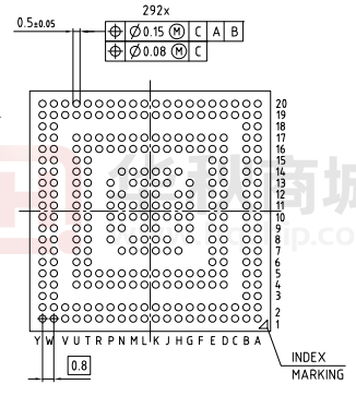


 工商网监
湘ICP备2023018690号
工商网监
湘ICP备2023018690号
