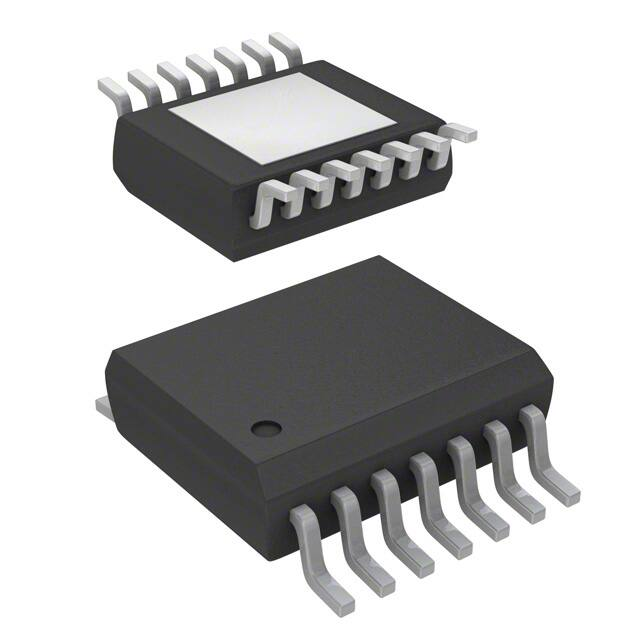
LITIX™ Basic
TLD1312EL
3 Channel High-Side Current Source
1
Package
PG-SSOP-14
Marking
TLD1312
Overview
Applications
•
Exterior LED lighting applications such as tail/brake light, turn indicator,
position light, side marker,...
•
Interior LED lighting applications such as ambient lighting, interior
illumination and dash board lighting.
GND
EN
Internal
supply
Thermal
protection
RSET
IN_SET
4.7nF**
4.7nF**
4.7nF**
ISO-Pulse
protection circuit
depending on
requirements
VS
CVS =4.7nF
BRAKE
10kΩ
Cmod =2.2µF
TAIL
OUT3
Output
control
Current
adjustment
OUT2
OUT1
TLD1312EL
GND
RPWMI
CPWMI
PWMI
** For EMI improvement if required
Application Diagram with TLD1312EL
Data Sheet
www.infineon.com
Rev. 1.2
2018-04-26
�LITIX™ Basic
TLD1312EL
Overview
Basic Features
•
3 Channel device with integrated output stages (current sources), optimized to drive LEDs with output
current up to 120 mA per channel
•
Low current consumption in sleep mode
•
PWM-operation supported via VS- and EN-pin
•
Integrated PWM dimming engine to provide two LED brightness levels without external logic (e.g. µC)
•
Output current adjustable via external low power resistor and possibility to connect PTC resistor for LED
protection during over temperature conditions
•
Reverse polarity protection and overload protection
•
Undervoltage detection
•
Wide temperature range: -40°C < Tj < 150°C
•
PG-SSOP-14 package with exposed heatslug
Description
The LITIX™ Basic TLD1312EL is a three channel high side driver IC with integrated output stages. It is designed
to control LEDs with a current up to 120 mA. In typical automotive applications the device is capable to drive
i.e. 3 red LEDs per chain (total 9 LEDs) with a current up to 60 mA, which is limited by thermal cooling aspects.
The output current is controlled practically independent of load and supply voltage changes.
Table 1
Product Summary
Parameter
Symbol
Value
Operating voltage range
VS(nom)
5.5 V ... 40 V
Maximum voltage
VS(max)
VOUTx(max)
40 V
Nominal output (load) current
IOUTx(nom)
60 mA when using a supply voltage range of 8 V - 18 V (e.g.
Automotive car battery). Currents up to IOUT(max) possible in
applications with low thermal resistance RthJA
Maximum output (load) current
IOUTx(max)
120 mA; depending on thermal resistance RthJA
Output current accuracy at RSET = 12 kΩ
kLT
750 ± 7%
Current consumption in sleep mode IS(sleep,typ)
0.1 µA
Protective Functions
•
ESD protection
•
Under voltage lock out
•
Over Load protection
•
Over Temperature protection
•
Reverse Polarity protection
Data Sheet
2
Rev. 1.2
2018-04-26
�LITIX™ Basic
TLD1312EL
Block Diagram
Block Diagram
VS
2
EN
Internal
supply
Thermal
protection
IN_SET
OUT3
Output
control
Current
adjustment
OUT2
OUT1
TLD1312EL
Figure 1
Data Sheet
GND
PWMI
Basic Block Diagram
3
Rev. 1.2
2018-04-26
�LITIX™ Basic
TLD1312EL
Pin Configuration
3
Pin Configuration
3.1
Pin Assignment
Figure 2
Data Sheet
VS
1
VS
2
EN
3
NC
4
PWMI
14
NC
13
OUT3
12
OUT2
11
OUT1
5
10
NC
IN_SET
6
9
GND
NC
7
8
NC
TLD1312EL
EP
Pin Configuration
4
Rev. 1.2
2018-04-26
�LITIX™ Basic
TLD1312EL
Pin Configuration
3.2
Pin Definitions and Functions
Pin
Symbol
Input/
Output
Function
1, 2
VS
–
Supply Voltage; battery supply, connect a decoupling capacitor (100 nF - 1 µF)
to GND
3
EN
I
Enable pin
4
NC
–
Pin not connected
5
PWMI
I/O
PWM Input
6
IN_SET
I/O
Input / SET pin; Connect a low power resistor to adjust the output current
7
NC
–
Pin not connected
8
NC
–
Pin not connected
–
1)
9
GND
Ground
10
NC
–
Pin not connected
11
OUT1
O
Output 1
12
OUT2
O
Output 2
13
OUT3
O
Output 3
14
NC
–
Pin not connected
–
1)
Exposed
Pad
GND
Exposed Pad; connect to GND in application
1) Connect all GND-pins together.
Data Sheet
5
Rev. 1.2
2018-04-26
�LITIX™ Basic
TLD1312EL
General Product Characteristics
4
General Product Characteristics
4.1
Absolute Maximum Ratings
Absolute Maximum Ratings 1)
Tj = -40°C to +150°C; all voltages with respect to ground, positive current flowing into pin for input pins (I),
positive currents flowing out of the I/O and output pins (O) (unless otherwise specified)
Pos.
Parameter
Symbol
Limit Values
Min.
Max.
Unit
Conditions
Voltages
4.1.1
Supply voltage
VS
-16
40
V
–
4.1.2
Input voltage EN
VEN
-16
40
V
–
4.1.3
Input voltage EN related to VS
VEN(VS)
VS - 40
VS + 16
V
–
4.1.4
Input voltage EN related to VOUTx
VEN - VOUTx
VEN VOUTx
-16
40
V
–
4.1.5
Output voltage
VOUTx
-1
40
V
–
4.1.6
Power stage voltage
VPS = VS - VOUTx
VPS
-16
40
V
–
4.1.7
Input voltage PWMI
VPWMI
-0.3
6
V
–
4.1.8
IN_SET voltage
VIN_SET
-0.3
6
V
–
4.1.9
IN_SET current
IIN_SET
–
2
mA
–
4.1.10
Output current
IOUTx
–
130
mA
–
Currents
Temperatures
4.1.11
Junction temperature
Tj
-40
150
°C
–
4.1.12
Storage temperature
Tstg
-55
150
°C
–
ESD Susceptibility
4.1.13
ESD resistivity to GND
VESD
-2
2
kV
Human Body
Model (100 pF via
1.5 kΩ)2)
4.1.14
ESD resistivity all pins to GND
VESD
-500
500
V
CDM3)
4.1.15
ESD resistivity corner pins to GND
VESD
-750
750
V
CDM3)
1) Not subject to production test, specified by design
2) ESD susceptibility, Human Body Model “HBM” according to ANSI/ESDA/JEDEC JS-001-2011
3) ESD susceptibility, Charged Device Model “CDM” according to JESD22-C101E
Note: Stresses above the ones listed here may cause permanent damage to the device. Exposure to absolute
maximum rating conditions for extended periods may affect device reliability.
Note: Integrated protection functions are designed to prevent IC destruction under fault conditions described in
the data sheet. Fault conditions are considered as “outside” normal operating range. Protection functions
are not designed for continuous repetitive operation.
Data Sheet
6
Rev. 1.2
2018-04-26
�LITIX™ Basic
TLD1312EL
General Product Characteristics
Functional Range
4.2
Pos.
Parameter
Symbol
Limit Values
Min.
Max.
Unit
Conditions
4.2.16
Supply voltage range for
normal operation
VS(nom)
5.5
40
V
–
4.2.17
Power on reset threshold
VS(POR)
–
5
V
VEN = VS
RSET = 12 kΩ
IOUTx = 80% IOUTx(nom)
VOUTx = 2.5 V
4.2.18
Junction temperature
Tj
-40
150
°C
–
Note: Within the functional range the IC operates as described in the circuit description. The electrical
characteristics are specified within the conditions given in the related electrical characteristics table.
Thermal Resistance
4.3
Pos.
Parameter
Symbol
4.3.1
Junction to Case
RthJC
4.3.2
Junction to Ambient 1s0p board
RthJA1
4.3.3
1)
2)
3)
4)
Junction to Ambient 2s2p board
Limit Values
Min.
Typ.
Max.
–
8
10
–
–
RthJA2
61
56
Unit
Conditions
K/W
1) 2)
K/W
1) 3)
–
–
Ta = 85 °C
Ta = 135 °C
K/W
1) 4)
–
45
–
Ta = 85 °C
–
43
–
Ta = 135 °C
Not subject to production test, specified by design. Based on simulation results.
Specified RthJC value is simulated at natural convection on a cold plate setup (all pins and the exposed Pad
are fixed to ambient temperature). Ta = 85°C, Total power dissipation 1.5 W.
The RthJA values are according to Jedec JESD51-3 at natural convection on 1s0p FR4 board. The product
(chip + package) was simulated on a 76.2 x 114.3 x 1.5 mm3 board with 70 µm Cu, 300 mm2 cooling area.
Total power dissipation 1.5 W distributed statically and homogenously over all power stages.
The RthJA values are according to Jedec JESD51-5,-7 at natural convection on 2s2p FR4 board. The product
(chip + package) was simulated on a 76.2 x 114.3 x 1.5 mm3 board with 2 inner copper layers (outside 2 x
70 µm Cu, inner 2 x 35 µm Cu). Where applicable, a thermal via array under the exposed pad contacted the
first inner copper layer. Total power dissipation 1.5 W distributed statically and homogenously over all
power stages.
Data Sheet
7
Rev. 1.2
2018-04-26
�LITIX™ Basic
TLD1312EL
EN Pin
5
EN Pin
The EN pin is a dual function pin:
Internal Supply
Output Control
EN
V EN
Figure 3
Block Diagram EN pin
Note: The current consumption at the EN-pin IEN needs to be added to the total device current consumption. The
total current consumption is the sum of the currents at the VS-pin IS and the EN-pin IEN.
5.1
EN Function
If the voltage at the pin EN is below a threshold of VEN(off) the LITIX™ Basic IC will enter Sleep mode. In this state
all internal functions are switched off, the current consumption is reduced to IS(sleep). A voltage above VEN(on) at
this pin enables the device after the Power on reset time tPOR.
VS
V EN
IOU T
t
t
tPOR
100%
80%
t
Figure 4
Data Sheet
Power on reset
8
Rev. 1.2
2018-04-26
�LITIX™ Basic
TLD1312EL
EN Pin
5.2
Internal Supply Pin
The EN pin can be used to supply the internal logic. There are two typical application conditions, where this
feature can be used:
1) In “DC/DC control Buck” configurations, where the voltage Vs can be below 5.5V.
2) In configurations, where a PWM signal is applied at the Vbatt pin of a light module. The buffer capacitor CBUF
is used to supply the LITIX™ Basic IC during Vbatt low (Vs low) periods. This feature can be used to minimize
the turn-on time to the values specified in Pos. 8.2.13. Otherwise, the power-on reset delay time tPOR
(Pos. 6.3.5) has to be considered.
The capacitor can be calculated using the following formula:
I EN LS
C BUF = tLOW max -------------------------------------------------V S – V D1 – V S POR
(1)
See also a typical application drawing in Chapter 9.
VBATT
VS
D1
GND
CBUF
EN
Internal
supply
Thermal
protection
Current
adjustment
OUT2
OUT1
LITIX™ Basic
Figure 5
Data Sheet
GND
R SET
IN_SET
OUT3
Output
control
External circuit when applying a fast PWM signal on VBATT
9
Rev. 1.2
2018-04-26
�LITIX™ Basic
TLD1312EL
EN Pin
V EN
t
V BATT
IOU T
t
tON (VS)
100%
80%
Switch off behavior depends on
V BATT and load characteristics
20%
t
Figure 6
Typical waveforms when applying a fast PWM signal on VBATT
The parameter tON(VS) is defined at Pos. 8.2.13. The parameter tOFF(VS) depends on the load and supply voltage
VBATT characteristics.
5.3
EN Unused
In case of an unused EN pin, there are two different ways to connect it:
5.3.1
EN - Pull Up to VS
The EN pin can be connected with a pull up resistor (e.g. 10 kΩ) to Vs potential. In this configuration the
LITIX™ Basic IC is always enabled.
5.3.2
EN - Direct Connection to VS
The EN pin can be connected directly to the VS pin (IC always enabled). This configuration has the advantage
(compared to the configuration described in Chapter 5.3.1) that no additional external component is
required.
Data Sheet
10
Rev. 1.2
2018-04-26
�LITIX™ Basic
TLD1312EL
PWMI Pin
6
PWMI Pin
The PWMI pin is designed as a dual function pin.
IPWMI(L)
Output Control
PWMI
VPWMI
Figure 7
Block Diagram PWMI pin
The pin can be used for PWM-dimming via a push-pull stage of a micro controller, which is connecting the
PWMI-pin to a low or high potential.
Note: The micro controller’s push-pull stage has to able to sink currents according to Pos. 6.3.15 to activate the
device.
Furthermore, the device offers also an internal PWM unit by connecting an external-RC network according to
Figure 10.
6.1
PWM Dimming
A PWM signal can be applied at the PWMI pin for LED brightness regulation of all 3 output stages. The dimming
frequency can be adjusted in a very wide range (e.g. 400 Hz). The PWMI pin is low active. Turn on/off thresholds
VPWMI(L) and VPWMI(H) are specified in parameters Pos. 6.3.12 and Pos. 6.3.13.
V PWMI
IOU T
tON (PWMI )
tOFF(PWMI )
t
100%
80%
20%
t
Figure 8
Data Sheet
Turn on and Turn off time for PWMI pin usage
11
Rev. 1.2
2018-04-26
�LITIX™ Basic
TLD1312EL
PWMI Pin
6.2
Internal PWM Unit
Connecting a resistor and a capacitor in parallel on the PWMI pin enables the internal pulse width modulation
unit. The following figure shows the charging and discharging defined by the RC-network according to
Figure 10 and the internal PWM unit.
VPWMI
Outputs OFF
VPWMI(H)
Internal PWM
VPWMI(L)
Outputs ON
t
OUTON
Figure 9
OUT - OFF
OUTON
OUT - OFF
OUTON
OUT - OFF
OUTON
OUT - OFF
PWMI operating voltages
The PWM Duty cycle (DC) and the PWM frequency can be adjusted using the formulas below. Please use only
typical values of VPWMI(L), VPWMI(H) and IPWMI(on) for the calculation of tPWMI(on) and tPWMI(off) (as described in
Pos. 6.3.12 to Pos. 6.3.15).
V PWMI H – I PWMI on R PWMI
-
t PWMI on = –R PWMI C PWMI LN ------------------------------------------------------------------------------ V PWMI L – I PWMI on R PWMI
(2)
V PWMI H
-
t PWMI off = R PWMI C PWMI LN ------------------------ V PWMI L
(3)
1
f PWMI = --------------------------------------------------------t PWMI on + tPWMI off
(4)
DC = tPWMI on f PWMI
(5)
Out of this equations the required CPWMI and RPWMI can be calculated:
t
t
PWMI off
PWMI on
------------------------
V PWMI L
– I PWMI on t PWMI off --------------------------
V PWMI H
–1
C PWMI = ------------------------------------------------------------------------------------------------------------------------------------------------------------------tPWMI on
-----------------------t
V PWMI L
V PWMI L PWMI off
LN -------------------------- V PWMI L --------------------------
– V PWMI H
V PWMI H
V PWMI H
t PWMI off
RPWMI = -------------------------------------------------------------- V PWMI H
-
C PWMI LN ------------------------ V PWMI L
Data Sheet
(6)
(7)
12
Rev. 1.2
2018-04-26
�LITIX™ Basic
TLD1312EL
PWMI Pin
See Figure 10 for a typical external circuitry.
Note: In case of junction temperatures above Tj(CRT) (Pos. 8.2.14) the device provides a temperature dependent
current reduction feature as descirbed in Chapter 8.1.1. In case of output current reduction IIN_SET is
reduced as well, which leads to increased turn on-times tPWMI(on), because the CPWMI is charged slower. The
turn off-time tPWMI(off) remains the same.
VBATT
VS
10 kΩ
EN
IN_SET
Thermal
protection
LITIX™ Basic
Figure 10
Data Sheet
OUT3
Output
control
Current
adjustment
RSET
CPWM I
RPWM I
PWMI
Internal
supply
OUT2
OUT1
GND
GND
Typical circuit using internal PWM unit
13
Rev. 1.2
2018-04-26
�LITIX™ Basic
TLD1312EL
PWMI Pin
6.3
Electrical Characteristics Internal Supply / EN / PWMI Pin
Electrical Characteristics Internal Supply / EN / PWMI pin
Unless otherwise specified: VS = 5.5 V to 40 V, Tj = -40°C to +150°C, RSET = 12 kΩ all voltages with respect to
ground, positive current flowing into pin for input pins (I), positive currents flowing out of the I/O and output
pins (O) (unless otherwise specified)
Pos.
Parameter
Symbol
6.3.1
Current consumption,
sleep mode
IS(sleep)
6.3.2
Current consumption,
active mode
IS(on)
Limit Values
Min.
Typ.
Max.
–
0.1
2
–
–
–
6.3.3
–
–
–
6.3.4
Current consumption,
device disabled via PWMI
–
–
–
Conditions
µA
1)
VEN = 0.5 V
Tj < 85 °C
VS = 18 V
VOUTx = 3.6 V
mA
2)
VPWMI= 0.5 V
IIN_SET = 0 µA
Tj < 105 °C
VS = 18 V
VOUTx = 3.6V
VEN = 5.5 V
VEN = 18 V
1)
REN = 10 kΩ between
VS and EN-pin
mA
2)
VS = 18 V
Tj < 105 °C
VIN_SET = 5 V
VEN = 5.5 V
VEN = 18 V
1)
REN = 10 kΩ between
VS and EN-pin
mA
2)
VS = 18 V
Tj < 105 °C
VPWMI= 3.4 V
VEN = 5.5 V
VEN = 18 V
1)
REN = 10 kΩ between
VS and EN-pin
1)
1.4
0.75
1.5
Current consumption,
IS(dis,IN_SET)
device disabled via IN_SET
–
–
–
Unit
1.4
0.7
1.4
IS(dis,PWMI)
–
–
–
–
–
–
1.6
0.75
1.6
Power-on reset delay time tPOR
–
–
25
µs
VS = VEN = 0 →13.5 V
VOUTx(nom) = 3.6 ± 0.3V
IOUTx = 80% IOUTx(nom)
6.3.6
Required supply voltage
for output activation
VS(on)
–
–
4
V
VEN = 5.5 V
VOUTx = 3 V
IOUTx = 50% IOUTx(nom)
6.3.7
Required supply voltage
for current control
VS(CC)
–
–
5.2
V
VEN = 5.5 V
VOUTx = 3.6 V
IOUTx ≥ 90% IOUTx(nom)
6.3.8
EN turn on threshold
VEN(on)
–
–
2.5
V
–
6.3.9
EN turn off threshold
VEN(off)
0.8
–
–
V
–
6.3.5
Data Sheet
3)
14
Rev. 1.2
2018-04-26
�LITIX™ Basic
TLD1312EL
PWMI Pin
Electrical Characteristics Internal Supply / EN / PWMI pin (cont’d)
Unless otherwise specified: VS = 5.5 V to 40 V, Tj = -40°C to +150°C, RSET = 12 kΩ all voltages with respect to
ground, positive current flowing into pin for input pins (I), positive currents flowing out of the I/O and output
pins (O) (unless otherwise specified)
Pos.
Parameter
Symbol
6.3.10
EN input current during
low supply voltage
IEN(LS)
6.3.11
EN high input current
IEN(H)
Limit Values
Min.
Typ.
Max.
–
–
1.8
–
–
–
–
–
–
–
–
0.1
0.1
1.65
0.45
Unit
Conditions
mA
1)
VS = 4.5 V
Tj < 105 °C
VEN = 5.5 V
mA
Tj < 105 °C
VS = 13.5 V, VEN = 5.5 V
VS = 18 V, VEN = 5.5 V
VS = VEN = 18 V
1)
VS = 18 V, REN = 10 kΩ
between VS and EN-pin
6.3.12
PWMI (active low)
Switching low threshold
(outputs on)
VPWMI(L)
1.5
1.85
2.3
V
1)4)
6.3.13
PWMI(active low)
Switching high threshold
(outputs off)
VPWMI(H)
2.45
2.85
3.2
V
1)4)5)
VS = 8...18 V
6.3.14
PWMI
∆VPWMI
Switching threshold
difference VPWMI(H) - VPWMI(L)
0.75
1
1.10
V
1)4)5)
VS = 8...18 V
6.3.15
PWMI (active low)
Low input current with
active channels (voltage