TLD5541-1
H-Bridge DC/DC Controller with SPI Interface
Infineon® LITIX™ Power Flex
1
Package
PG-VQFN-48-31
PG-TQFP-48-9
Marking
TLD55411QV
TLD55411QU
Sales Name
TLD5541-1QV
TLD5541-1QU
Overview
Features
•
Single Inductor high power Buck-Boost controller
•
Wide LED forward voltage Range (2 V up to 55 V)
•
Wide VIN Range (IC 4.5 V to 40 V, Power 4.5 V to 55 V)
•
Switching Frequency Range from 200 kHz to 700 kHz
•
SPI for diagnostics and control
•
Maximum Efficiency in every condition (up to 96%)
•
Constant Current (LED) and Constant Voltage Regulation
•
Drives Multiple Load with a single IC thanks to the Fast Output Discharge operation
•
Limp Home Function (Fail Safe Mode)
•
EMC optimized device: Features an auto Spread Spectrum
•
LED and Input current sense with dedicated monitor Outputs
•
Advanced protection features for device and load
•
Enhanced Dimming features: Analog and PWM dimming
•
LED current accuracy +/- 3%
•
Available in a small thermally enhanced PG-VQFN-48-31 or PG-TQFP-48-9 package
•
Automotive AEC Qualified
RIIN
CIN2
CIN1
Cfilter
R1
VDD
R4
LIMPHOME
IVCC
IIN1
SET
LHI
EN/INUVLO
R2
RCOMP
FAIL SA FE Circuit
RFREQ
RSYNC
GND
Figure 1
Datasheet
RSI
RSO
RSCLK
M1
M3
COUT1
RFB
COUT3
SWCS
FREQ
VDD
M4
LOUT
M2
SOFT_START
CSN
SI
SO
SCLK
CBST1 CBST2
LSGD1
COMP
PWMI
IINMON
IOUTMON
SYNC
RPWMI
RSENSE
RSENSE
VDD
SPI
SPI
INOVLO
CCOMP
PWM I_LH
RCSN
HSGD1
SWN1
CSOFT_START
Micro
controller
I/O
A/D
A/D
I/O
R3
REN
RPD
I/O
COUT2
BST1
BST2
FAIL SAFE Circuit
D2
D1
RVFBH
R5
Rfilter
CIVCC
IVCC_ext
VIN
IIN2
RVFBL
IVCC
RSWCS
VIN
SGND
PGND1
PGND2
LSGD2
SWN2
HSGD2
VFB
FBH
FBL
VSS
AGND
Application Drawing - TLD5541-1 as current regulator
www.infineon.com
1
Rev. 1.1
2018-02-08
�TLD5541-1
H-Bridge DC/DC Controller with SPI Interface
Overview
Description
The TLD5541-1 is a synchronous MOSFET H-Bridge DC/DC controller with built in protection features and SPI
interface. This concept is beneficial for driving high power LEDs with maximum system efficiency and
minimum number of external components. The TLD5541-1 offers both analog and digital (PWM) dimming.The
switching frequency is adjustable in the range of 200 kHz to 700 kHz. It can be synchronized to an external
clock source. A built in programable Spread Spectrum switching frequency modulation and the forced
continuous current regulation mode improve the overall EMC behavior. Furthermore the current mode
regulation scheme provides a stable regulation loop maintained by small external compensation
components. The adjustable soft start feature limits the current peak as well as voltage overshoot at start-up.
The TLD5541-1 is suitable for use in the harsh automotive environment.
Table 1
Product Summary
Power Stage input voltage range
VPOW
4.5 V … 55 V
Device Input supply voltage range
VVIN
4.5 V … 40 V
Maximum output voltage (depending by the
application conditions)
VOUT(max)
55 V as LED Driver Boost Mode
50 V as LED Driver Buck Mode
50 V as Voltage regulator
Switching Frequency range
fSW
200 kHz... 700 kHz
Typical NMOS driver on-state resistance at
Tj = 25°C (Gate Pull Up)
RDS(ON_PU)
2.3 Ω
Typical NMOS driver on-state resistance at
Tj = 25°C (Gate Pull Down)
RDS(ON_PD)
1.2 Ω
SPI clock frequency
fSCLK(MAX)
5 MHz
Protective Functions
•
Over load protection of external MOSFETs
•
Shorted load, open load, output overvoltage protection
•
Input overvoltage and undervoltage protection
•
Thermal shutdown of device with autorestart behavior
•
Electrostatic discharge protection (ESD)
Diagnostic Functions
•
Latched diagnostic information via SPI
•
Open load detection in ON-state
•
Device Overtemperature shutdown and Temperature Prewarning
•
Smart monitoring and advanced functions provide ILED and IIN information
Limp Home Function
•
Limp Home activation via LHI pin
Applications
•
Especially designed for driving high power LEDs in automotive applications
•
Automotive Exterior Lighting: full LED headlamp assemblies (Low Beam, High Beam, Matrix Beam, Pixel
Light)
•
General purpose current/voltage controlled DC/DC LED driver
Datasheet
2
Rev. 1.1
2018-02-08
�TLD5541-1
H-Bridge DC/DC Controller with SPI Interface
Block Diagram
2
Block Diagram
IVCC
Internal Supply
LDO
VIN
SYNC
Oscillator
Auto-Spread
Spectrum
Generator
VI N
Voltage
Prot ection
+ Enable
BUCK
LO GIC
IVCC_EXT
LSGD1
PWM
Generator
Diagnosis Open Load + Short
to GND
IVCC_EXT
Soft Start
Limp Home Mode
LHI
PGND2
BOOST
LOGIC
Analog Dimming Pin
Fast Output
Discharge
Operation
Mode
SWN2
Output
current
accuracy
calibration
HSGD2
BST2
Switch Current
Error Amplifier
VDD
CSN
8 Bit DAC
Analog
Dimming
SPI
SCLK
PGND1
LSGD2
Digital Dimming
PWMI
SET
SWN1
Thermal Protection
+ Prewarning
SOFT_START
BST1
HSGD1
Slope Comp.
INOVLO
IVCC_EXT
GATE
DRIVER
FREQ
EN/INUVLO
Power
On Reset
Voltage Loop
Feedback
SWCS
SGND
VFB
SI
SO
Input
Current
Monitor
Input/diag nosis
regi ster
LED
Current
Monitor
FBH
Feedback Error Amplifier
Figure 2
Datasheet
AGND
IIN1 IIN2
IOUTMON
VSS
IINMON
FBL
COMP
Block Diagram - TLD5541-1
3
Rev. 1.1
2018-02-08
�TLD5541-1
H-Bridge DC/DC Controller with SPI Interface
Pin Configuration
3
Pin Configuration
3.1
Pin Assignment
Figure 3
Pin Configuration - TLD5541-1
Datasheet
4
Rev. 1.1
2018-02-08
�TLD5541-1
H-Bridge DC/DC Controller with SPI Interface
Pin Configuration
3.2
Pin
Pin Definitions and Functions
Symbol
I/O
1)
Function
Power Supply
1, 12,
n.c.
15, 21,
32, 33,
45, 48
-
Not connected, tie to AGND on the Layout;
44
VIN
-
Power Supply Voltage;
Supply for internal biasing.
31
VDD
-
Digital GPIO Supply Voltage;
Connect to reverse voltage protected 5 V or 3.3 V supply.
47
IVCC_EXT
I
PD External LDO input;
Input to alternatively supply internal Gate Drivers via an external LDO.
Connect to IVCC pin to use internal LDO to supply gate drivers. Must not
be left open.
5, 8
PGND1, 2
-
Power Ground;
Ground for power potential. Connect externally close to the chip.
26
VSS
-
Digital GPIO Ground;
Ground for GPIO pins.
40
AGND
-
Analog Ground;
Ground Reference
-
EP
-
Exposed Pad;
Connect to external heatspreading Cu area (e.g. inner GND layer of
multilayer PCB with thermal vias).
Gate Driver Stages
2
HSGD1
O
Highside Gate Driver Output 1;
Drives the top n-channel MOSFET with a voltage equal to VIVCC_EXT
superimposed on the switch node voltage SWN1. Connect to gate of
external switching MOSFET.
11
HSGD2
O
Highside Gate Driver Output 2;
Drives the top n-channel MOSFET with a voltage equal to VIVCC_EXT
superimposed on the switch node voltage SWN2. Connect to gate of
external switching MOSFET.
6
LSGD1
O
Lowside Gate Driver Output 1;
Drives the lowside n-channel MOSFET between GND and VIVCC_EXT.
Connect to gate of external switching MOSFET.
7
LSGD2
O
Lowside Gate Driver Output 2;
Drives the lowside n-channel MOSFET between GND and VIVCC_EXT.
Connect to gate of external switching MOSFET.
4
SWN1
IO
Switch Node 1;
SWN1 pin swings from a diode voltage drop below ground up to VIN.
9
SWN2
IO
Switch Node 2;
SWN2 pin swings from ground up to a diode voltage drop above VOUT.
Datasheet
5
Rev. 1.1
2018-02-08
�TLD5541-1
H-Bridge DC/DC Controller with SPI Interface
Pin Configuration
Pin
Symbol
I/O
46
IVCC
O
1)
Function
Internal LDO output;
Used for internal biasing and gate driver supply. Bypass with external
capacitor close to the pin. Pin must not be left open.
Inputs and Outputs
37
LHI
I
23
TEST1
-
Test Pin;
Used for Infineon end of line test, connect to GND in application.
25
TEST2
-
Test Pin;
Used for Infineon end of line test, connect to GND in application.
41
EN/INUVLO
I
35
FREQ
I
34
SYNC
I
PD Synchronization Input;
Apply external clock signal for synchronization.
24
PWMI
I
PD Control Input; Digital input 5 V or 3.3 V.
13
FBH
I
Output current Feedback Positive;
Non inverting Input (+).
14
FBL
I
Output current Feedback Negative;
Inverting Input (-).
3
BST1
IO
Bootstrap capacitor;
Used for internal biasing and to drive the Highside Switch HSGD1.
Bypass to SWN1 with external capacitor close to the pin. Pin must not be
left open.
10
BST2
IO
Bootstrap capacitor;
Used for internal biasing and to drive the Highside Switch HSGD2.
Bypass to SWN2 with external capacitor close to the pin. Pin must not be
left open.
17
SWCS
I
Current Sense Input;
Inductor current measurement - Non Inverting Input (+).
18
SGND
I
Current Sense Ground;
Inductor current sense - Inverting Input (-).
Route as Differential net with SWCS on the Layout.
42
IIN1
I
Input Current Monitor Positive;
Non Inverting Input (+), connect to VIN if input current monitor is not
needed.
43
IIN2
I
Input Current Monitor Negative;
Inverting Input (-), connect to VIN if input current monitor is not needed.
19
COMP
O
Compensation Network Pin;
Connect R and C network to pin for stability phase margin adjustment.
Datasheet
PD Limp Home Input Pin;
Used to enter in Limp Home state during Fail Safe condition.
PD Enable/Input Under Voltage Lock Out;
Used to put the device in a low current consumption mode, with
additional capability to fix an undervoltage threshold via external
components. Pin must not be left open.
Frequency Select Input;
Connect external resistor to GND to set frequency.
6
Rev. 1.1
2018-02-08
�TLD5541-1
H-Bridge DC/DC Controller with SPI Interface
Pin Configuration
1)
Pin
Symbol
I/O
Function
38
SOFT_START
O
Softstart configuration Pin;
Connect a capacitor CSOFT_START to GND to fix a soft start ramp default
time.
36
INOVLO
I
Input Overvoltage Protection Pin;
Define an upper voltage threshold and switches OFF the device in case
of overvoltages on the VIN supply. Must not be left open.
20
VFB
I
Voltage Loop Feedback Pin;
VFB is intended to set output protection functions.
22
SET
I
Analog current sense adjustment Pin;
39
IINMON
O
Input current monitor output;
Monitor pin that produces a voltage that is 20 times the voltage VIN1-IN2.
IINMON will be equal 1 V when VIIN1-VIIN2 = 50 mV.
16
IOUTMON
O
Output current monitor output;
Monitor pin that produces a voltage that is 200 mV + 8 times the voltage
VFBH-FBL. IOUTMON will be equal 1.4 V when VFBH-FBL = 150 mV.
30
SI
I
PD Serial data in; Digital input 5 V or 3.3 V.
29
SCLK
I
PD Serial clock; Digital input 5 V or 3.3 V.
28
CSN
I
PU SPI chip select; Digital input 5 V or 3.3 V. Active LOW.
27
SO
O
Serial data out; Digital output, referenced to VDD.
SPI
1) O: Output, I: Input,
PD: pull-down circuit integrated,
PU: pull-up circuit integrated
Datasheet
7
Rev. 1.1
2018-02-08
�TLD5541-1
H-Bridge DC/DC Controller with SPI Interface
General Product Characteristics
4
General Product Characteristics
4.1
Absolute Maximum Ratings
Table 2
Absolute Maximum Ratings1)
TJ = -40°C to +150°C; all voltages with respect to AGND, (unless otherwise specified)
Parameter
Symbol
Values
Min.
Typ. Max.
Unit Note or
Test Condition
Number
Supply Voltages
VIN
Supply Input
VVIN
-0.3
–
60
V
–
P_4.1.1
VDD
Digital supply voltage
VVDD
-0.3
–
6
V
–
P_4.1.2
IVCC
Internal Linear Voltage Regulator
Output voltage
VIVCC
-0.3
–
6
V
–
P_4.1.3
-0.3
–
6
V
–
P_4.1.4
-0.3
–
5.5
V
–
P_4.1.54
-0.3
–
5.5
V
–
P_4.1.55
IVCC_EXT
VIVCC_EXT
External Linear Voltage Regulator Input
voltage
Gate Driver Stages
LSGD1,2 - PGND1,2
Lowside Gatedriver voltage
VLSGD1,2-
HSGD1,2 - SWN1,2
Highside Gatedriver voltage
VHSGD1,2-
SWN1, SWN2
switching node voltage
VSWN1, 2
-1
–
60
V
–
P_4.1.6
(BST1-SWN1), (BST2-SWN2)
Boostrap voltage
VBST1,2-
-0.3
–
6
V
–
P_4.1.7
BST1, BST2
Boostrap voltage related to GND
VBST1, 2
-0.3
–
65
V
–
P_4.1.8
SWCS
Switch Current Sense Input voltage
VSWCS
-0.3
–
0.3
V
–
P_4.1.9
SGND
Switch Current Sense GND voltage
VSGND
-0.3
–
0.3
V
–
P_4.1.10
SWCS-SGND
Switch Current Sense differential
voltage
VSWCS-
-0.5
–
0.5
V
–
P_4.1.11
PGND1,2
Power GND voltage
VPGND1,2
-0.3
–
0.3
V
–
P_4.1.28
VIIN1, 2
-0.3
–
60
V
–
P_4.1.12
PGND1,2
SWN1,2
SWN1,2
SGND
High voltage Pins
IIN1, IIN2
Input Current monitor voltage
Datasheet
8
Rev. 1.1
2018-02-08
�TLD5541-1
H-Bridge DC/DC Controller with SPI Interface
General Product Characteristics
Table 2
Absolute Maximum Ratings1) (cont’d)
TJ = -40°C to +150°C; all voltages with respect to AGND, (unless otherwise specified)
Parameter
Symbol
Values
Min.
Typ. Max.
Unit Note or
Test Condition
Number
IIN1-IIN2
Input Current monitor differential
voltage
VIIN1-IIN2
-0.5
–
0.5
V
–
P_4.1.13
FBH, FBL
Feedback Error Amplifier voltage
VFBH, FBL
-0.3
–
60
V
–
P_4.1.14
FBH-FBL
Feedback Error Amplifier differential
voltage
VFBH-FBL
-0.5
–
0.5
V
–
P_4.1.15
EN/INUVLO
Device enable/input undervoltage
lockout
VEN/INUVLO -0.3
–
60
V
–
P_4.1.16
PWMI
Digital Input voltage
VPWMI
-0.3
–
5.5
V
–
P_4.1.17
CSN
Voltage at Chip Select pin
VCSN
-0.3
–
5.5
V
–
P_4.1.18
SCLK
Voltage at Serial Clock pin
VSCLK
-0.3
–
5.5
V
–
P_4.1.19
SI
Voltage at Serial Input pin
VSI
-0.3
–
5.5
V
–
P_4.1.20
SO
Voltage at Serial Output pin
VSO
-0.3
–
5.5
V
–
P_4.1.21
SYNC
Synchronization Input voltage
VSYNC
-0.3
–
5.5
V
–
P_4.1.22
LHI
Limp Home Input Voltage
VLHI
-0.3
–
5.5
V
–
P_4.1.58
VFB
Loop Input voltage
VVFB
-0.3
–
5.5
V
–
P_4.1.25
INOVLO
Input overvoltage lockout
VINOVLO
-0.3
–
5.5
V
–
P_4.1.26
SET
Analog dimming Input voltage
VSET
-0.3
–
5.5
V
–
P_4.1.29
COMP
Compensation Input voltage
VCOMP
-0.3
–
3.6
V
–
P_4.1.30
SOFT_START
Softstart Voltage
VSOFT_STAR -0.3
–
3.6
V
–
P_4.1.31
FREQ
Voltage at frequency selection pin
VFREQ
–
3.6
V
–
P_4.1.32
Digital (I/O) Pins
Analog Pins
Datasheet
T
-0.3
9
Rev. 1.1
2018-02-08
�TLD5541-1
H-Bridge DC/DC Controller with SPI Interface
General Product Characteristics
Table 2
Absolute Maximum Ratings1) (cont’d)
TJ = -40°C to +150°C; all voltages with respect to AGND, (unless otherwise specified)
Parameter
Symbol
Values
Min.
Typ. Max.
Unit Note or
Test Condition
Number
IINMON
Voltage at input monitor pin
VIINMON
-0.3
–
3.6
V
–
P_4.1.33
IOUTMON
Voltage at output monitor pin
VIOUTMON
-0.3
–
5.5
V
–
P_4.1.34
Junction Temperature
Tj
-40
–
150
°C
–
P_4.1.35
Storage Temperature
Tstg
-55
–
150
°C
–
P_4.1.36
VESD,HBM
-2
–
2
kV
HBM2)
P_4.1.37
3)
P_4.1.38
3)
P_4.1.39
Temperatures
ESD Susceptibility
ESD Resistivity of all Pins
ESD Resistivity to GND
VESD,CDM
ESD Resistivity of corner Pins to GND
-500
VESD,CDM_c -750
–
500
–
V
750
CDM
V
CDM
orner
1) Not subject to production test, specified by design.
2) ESD susceptibility, HBM according to ANSI/ESDA/JEDEC JS001 (1.5 kΩ, 100 pF)
3) ESD susceptibility, Charged Device Model “CDM” ESDA STM5.3.1 or ANSI/ESD S.5.3.1
Note:
Stresses above the ones listed here may cause permanent damage to the device. Exposure to
absolute maximum rating conditions for extended periods may affect device reliability.
Integrated protection functions are designed to prevent IC destruction under fault conditions
described in the datasheet. Fault conditions are considered as “outside” normal operating range.
Protection functions are not designed for continuous repetitive operation.
4.2
Functional Range
Table 3
Functional Range
Parameter
Symbol
Values
Min.
Typ. Max.
Unit Note or
Test Condition
Number
Device Extended Supply Voltage
Range
VVIN
4.5
–
40
V
1)
P_4.2.1
Device Nominal Supply Voltage
Range
VVIN
8
–
36
V
–
P_4.2.2
Power Stage Voltage Range
VPOW
4.5
–
55
V
1)
P_4.2.5
Digital Supply Voltage
VDD
3
–
5.5
V
–
P_4.2.3
Junction Temperature
Tj
-40
–
150
°C
–
P_4.2.4
1) Not subject to production test, specified by design.
Datasheet
10
Rev. 1.1
2018-02-08
�TLD5541-1
H-Bridge DC/DC Controller with SPI Interface
General Product Characteristics
Note:
Within the functional range the IC operates as described in the circuit description. The electrical
characteristics are specified within the conditions given in the related electrical characteristics
table.
4.3
Thermal Resistance
Note:
This thermal data was generated in accordance with JEDEC JESD51 standards. For more
information, go to www.jedec.org.
Table 4
Parameter
Junction to Case
Junction to Ambient
Symbol
RthJC
RthJA
Values
Min.
Typ.
Max.
–
0.9
–
–
25
–
Unit
Note or
Test Condition
Number
K/W
1) 2)
P_4.3.1
K/W
3)
P_4.3.2
2s2p
1) Not subject to production test, specified by design.
2) Specified RthJC value is simulated at natural convection on a cold plate setup (all pins and the exposed pad are fixed
to ambient temperature). Ta = 25°C; The IC is dissipating 1 W.
3) Specified RthJA value is according to JEDEC 2s2p (JESD 51-7) + (JESD 51-5) and JEDEC 1s0p (JESD 51-3) + heatsink area
at natural convection on FR4 board; The device was simulated on a 76.2 x 114.3 x 1.5 mm board. The 2s2p board has
2 outer copper layers (2 x 70 µm Cu) and 2 inner copper layers (2 x 35 µm Cu). A thermal via (diameter = 0.3 mm and
25 µm plating) array was applied under the exposed pad and connected the first outer layer (top) to the first inner
layer and second outer layer (bottom) of the JEDEC PCB. Ta = 25°C; The IC is dissipating 1 W.
Datasheet
11
Rev. 1.1
2018-02-08
�TLD5541-1
H-Bridge DC/DC Controller with SPI Interface
Power Supply
5
Power Supply
The TLD5541-1 is supplied by the following pins:
•
VIN (main supply voltage)
•
VDD (digital supply voltage)
•
IVCC_EXT (supply for internal gate driver stages)
The VIN supply, in combination with the VDD supply, provides internal supply voltages for the analog and
digital blocks. In situations where VIN voltage drops below VDD voltage, an increased current consumption
may be observed at the VDD pin.
The SPI and IO interfaces are supplied by the VDD pin.
IVCC_EXT is the supply for the low side driver stages. This supply is used also to charge, through external
Schottky diodes, the bootstrap capacitors which provide supply voltages to the high side driver stages. If no
external voltage is available this pin must be shorted to IVCC, which is the output of an internal 5 V LDO.
The supply pins VIN, VDD and IVCC_EXT have undervoltage detections.
Undervoltage on VDD supply voltage prevents the activation of the gate driver stages and any SPI
communication (the SPI registers are reset). Undervoltage on IVCC_EXT or IVCC voltages forces a deactivation
of the driver stages, thus stopping the switching activity, but has no effect on the SPI register settings.
Moreover the double function pin EN/INUVLO can be used as an input undervoltage protection by placing a
resistor divider from VIN to GND (refer to Chapter 10.3).
If EN/INUVLO undervoltage is detected, it will turn-off the IVCC voltage regulator, stop switching, stop
communications and reset all the registers.
Figure 4 shows a basic concept drawing of the supply domains and interactions among pins VIN, VDD and
IVCC/IVCC_EXT.
VIN
VREG (5V)
R1
EN/INUVLO
IVCC
Internal pre-regulated
voltage Supply
Undervoltage
detection
R2
IVCC_EXT
VREG
digital
VREG
analog
LS - Drivers
PGND
Undervoltage
detection
BSTx
Bandgap
Reference
VDD
Figure 4
Datasheet
SPI & I/O
Register
Banks
HS - Drivers
LOGIC
SWNx
Power Supply Concept Drawing
12
Rev. 1.1
2018-02-08
�TLD5541-1
H-Bridge DC/DC Controller with SPI Interface
Power Supply
Usage of EN/INUVLO pin in different applications
The pin EN/INUVLO is a double function pin and can be used to put the device into a low current consumption
mode. An undervoltage threshold should be fixed by placing an external resistor divider (A) in order to avoid
low voltage operating conditions. This pin can be driven by a µC-port as shown in (B) .
A
B
Vin
Vin
VIN
VIN
R1
R1
EN/INUVLO
R2
Figure 5
Datasheet
GND
EN/INUVLO
µC Port
R2
GND
Usage of EN/INUVLO pin in different applications
13
Rev. 1.1
2018-02-08
�TLD5541-1
H-Bridge DC/DC Controller with SPI Interface
Power Supply
5.1
Different Power States
TLD5541-1 has the following power states:
•
SLEEP state
•
IDLE state
•
LIMP HOME state
•
ACTIVE state
The transition between the power states is determined according to these variables after a filter time of max.
3 clock cycles:
•
VIN level
•
EN/INUVLO level
•
IVCC level
•
IVCC_EXT level
•
VDD level
•
LHI level
•
DVCCTRL.IDLE bit state
The state diagram including the possible transitions is shown in Figure 6.
The Power-up condition is entered when the supply voltage VVIN exceed its minimum supply voltage threshold
VVIN(ON).
SLEEP
When the device is powered it enters the SLEEP state, all outputs are OFF and the SPI registers are reset,
independently from the supply voltages at the pins VIN , VDD, IVCC, and IVCC_EXT. The current consumption
is low. Refer to parameters: IVDD(SLEEP), and IVIN(SLEEP).
The transition from SLEEP to ACTIVE state requires a specified time: tACTIVE.
IDLE
In IDLE state, the current consumption of the device can reach the limits given by parameter IVDD (P_5.3.4). The
internal voltage regulator is working. Not all diagnosis functions are available (refer to Chapter 10 for
additional informations). In this state there is no switching activity, independently from the supply voltages
VIN, VDD, IVCC and IVCC_EXT. When VDD is available, the SPI registers are working and SPI communication is
possible.
Limp Home
The Limp Home state is beneficial to fulfill system safety requirements and provides the possibility to
maintain a defined current/voltage level on the output via a backup control circuitry. The backup control
circuitry turns on required loads during a malfunction of the µC. For detailed info, refer to Chapter 8.
When Limp Home state is entered, SPI registers are reset to their default values and SPI communication is
possible but only in read mode (SPI registers can be read but cannot be written). In order to regulate the
output current/voltage, it is necessary that VIN and IVCC_EXT are present and above their undervoltage
threshold.
ACTIVE
In active state the device will start switching activity to provide power at the output only when PWMI = HIGH.
To start the Highside gate drivers HSGD1,2 the voltage level VBST1,2 - VSWN1,2 needs to be above the threshold
Datasheet
14
Rev. 1.1
2018-02-08
�TLD5541-1
H-Bridge DC/DC Controller with SPI Interface
Power Supply
VBST1,2 - VSWN1,2_UVth. In ACTIVE state the device current consumption via VIN and VDD is dependent on the
external MOSFET used and the switching frequency fSW.
Power-up
LHI = LOW
& EN/INUVLO = HIGH
EN/INUVLO = LOW
SLEEP
EN/INUVLO = LOW
LHI = HIGH
& EN/INUVLO = HIGH
EN/INUVLO = LOW
LHI = HIGH
IDLE
VIN = HIGH
& IVCC = HIGH
& IVCC_EXT = HIGH
& VDD = HIGH
& DVCCTRL.IDLE = LOW
VIN = LOW
or IVCC = LOW
or IVCC_EXT = LOW
or VDD = LOW
or DVCCTRL.IDLE = HIGH
LIMP HOME
EN/INUVLO = LOW
LHI = LOW
ACTIVE
LHI = HIGH
Figure 6
Simplified State Diagram
5.2
Different Possibilities to RESET the device
There are several reset triggers implemented in the device.
After any kind of reset, the Transmission Error Flag (TER) is set to HIGH.
Under Voltage Reset:
EN/INUVLO: When EN/INUVLO is below VEN/INUVLOth (P_5.3.7), the SPI interface is not working and all the
registers are reset to their default values. In addition, the device enters SLEEP mode and the current
consumption is minimized.
VDD: When VVDD is below VVDD(UV) (P_5.3.6), the SPI interface is not working and all the registers are reset to their
default values.
Reset via SPI command:
There is a command (DVCCTRL.SWRST = HIGH) available to RESET all writeable registers to their default
values. Note that the result coming from the Calibration routine, which is readable by the SPI when
DVCCTRL.ENCAL = HIGH, is not reset by the SWRST.
Reset via Limp Home:
When Limp Home state is detected the registers are reset to the default values.
Datasheet
15
Rev. 1.1
2018-02-08
�TLD5541-1
H-Bridge DC/DC Controller with SPI Interface
Power Supply
5.3
Electrical Characteristics
Table 5
EC Power Supply
VIN = 8 V to 36 V, TJ = -40°C to +150°C, all voltages with respect to AGND; (unless otherwise specified)
Parameter
Symbol
Values
Unit
Note or
Test Condition
Number
Min.
Typ.
Max.
VVIN(ON)
–
–
4.7
V
VIN increasing;
VEN/INUVLO = HIGH;
VDD = 5 V;
IVCC = IVCC_EXT =
10 mA;
P_5.3.1
Input Undervoltage switch OFF VVIN(OFF)
–
–
4.5
V
VIN decreasing;
VEN/INUVLO = HIGH;
VDD = 5 V;
IVCC = IVCC_EXT =
10 mA;
P_5.3.14
Device operating current
IVIN(ACTIVE)
–
4.4
6
mA
1)
ACTIVE mode;
VPWMI = 0 V;
P_5.3.2
VIN Sleep mode supply current
IVIN(SLEEP)
–
–
1.5
µA
VEN/INUVLO = 0 V;
VCSN = VDD = 5 V;
VIN = 13.5 V;
VIVCC = VIVCC_EXT= 0 V;
P_5.3.3
Digital supply current
IVDD
–
–
0.5
mA
VIN = 13.5 V;
fSCLK = 0 Hz;
VPWMI = 0 V;
VEN =VCSN = VDD = 5 V;
P_5.3.4
Digital Supply Sleep mode
current
IVDD(SLEEP)
–
–
1.5
µA
VEN/INUVLO = 0 V;
VCSN = VDD = 5 V;
VIN = 13.5 V;
VIVCC = VIVCC_EXT = 0 V;
P_5.3.5
Undervoltage shutdown
threshold voltage
VVDD(UV)
1
–
3
V
VCSN = VDD;
P_5.3.6
VSI = VSCLK = 0 V;
SO from LOW to HIGH
impedance;
Power Supply VIN
Input Voltage Startup
Digital Power Supply VDD
EN/INUVLO Pin characteristics
Input Undervoltage falling
Threshold
VEN/INUVLOth 1.6
1.75
1.9
V
–
P_5.3.7
EN/INUVLO Rising Hysteresis
VEN/INUVLO(hy –
90
–
mV
1)
P_5.3.8
0.89
1.34
µA
VEN/INUVLO = 0.8 V;
P_5.3.9
st)
EN/INUVLO input Current LOW IEN/INUVLO(LO 0.45
W)
Datasheet
16
Rev. 1.1
2018-02-08
�TLD5541-1
H-Bridge DC/DC Controller with SPI Interface
Power Supply
Table 5
EC Power Supply (cont’d)
VIN = 8 V to 36 V, TJ = -40°C to +150°C, all voltages with respect to AGND; (unless otherwise specified)
Parameter
Symbol
Values
Min.
EN/INUVLO input Current HIGH IEN/INUVLO(HI 1.1
Unit
Note or
Test Condition
Number
Typ.
Max.
2.2
3.3
µA
VEN/INUVLO = 2 V;
P_5.3.10
GH)
LHI Pin characteristics
LOW level
VLHI(L)
0
-
0.8
V
–
P_5.3.16
HIGH level
VLHI(H)
2.0
-
5.5
V
–
P_5.3.17
L-Input pull-down current
ILHI(L)
6
12
18
μA
VLHI = 0.8 V;
P_5.3.18
H-Input pull-down current
ILHI(H)
15
30
45
μA
VLHI = 2.0 V;
P_5.3.19
tACTIVE
–
–
0.7
ms
1)
P_5.3.11
Timings
SLEEP mode to ACTIVE time
VIVCC = VIVCC_EXT;
CIVCC = 10 µF;
VIN = 13.5 V;
VDD = 5 V;
1) Not subject to production test, specified by design.
Datasheet
17
Rev. 1.1
2018-02-08
�TLD5541-1
H-Bridge DC/DC Controller with SPI Interface
Regulator Description
6
Regulator Description
The TLD5541-1 includes all of the functions necessary to provide constant current to the output as usually
required to drive LEDs. A voltage mode regulation can also be implemented (Refer to Chapter 6.7).
It is designed to control 4 gate driver outputs in a H-Bridge topology by using only one inductor and 4 external
MOSFETs. This topology is able to operate in high power BOOST, BUCK-BOOST and BUCK mode applications
with maximum efficiency.
The transition between the different regulation modes is done automatically by the device itself, with respect
to the application boundary conditions.
The transition phase between modes is seamless.
A SPI flag provides mode feedback to the µC (refer to SPI bits REGUSETMON.REGUMODFB).
6.1
Regulator Diagram Description
The TLD5541-1 includes two analog current control inputs (IIN1, IIN2) to limit the maximum Input current
(Block A1 and A7 in Figure 7).
A second analog current control loop (A5, A6 with complessive gain = IFBxgm) connected to the sensing pins
FBL, FBH regulates the output current.
The regulator function is implemented by a pulse width modulated (PWM) current mode controller. The error
in the output current loop is used to determine the appropriate duty cycle to get a constant output current.
An external compensation network (RCOMP, CCOMP) is used to adjust the control loop to various application
boundary conditions.
The inductor current for the current mode loop is sensed by the RSWCS resistor.
RSWCS is used also to limit the maximum external switches / inductor current.
If the Voltage across RSWCS exceeds its overcurrent threshold (VSWCS_buck or VSWCS_boost for buck or boost
operation respectively) the device reduces the duty cycle in order to bring the switches current below the
imposed limit.
The current mode controller has a built-in slope compensation as well to prevent sub-harmonic oscillations.
The control loop logic block (LOGIC) provides a PWM signal to four internal gate drivers. The gate drivers
(HSGD1,2 and LSGD1,2) are used to drive external MOSFETs in an H-Bridge setup . Once the soft start expires
a forced CCM regulation mode is performed.
The control loop block diagram displayed in Figure 7 shows a typical constant current application. The voltage
across RFB sets the output current. RIN is used to fix the maximum input current.
The output current is fixed via the SPI parameter (LEDCURRADIM.ADIMVAL = 11110000B = default at 100%)
plus an offset trimming (LEDCURRCAL.CALIBVAL = 0000B = default in the middle of the range). Refer to
Chapter 8.1 for more details.
Datasheet
18
Rev. 1.1
2018-02-08
�TLD5541-1
H-Bridge DC/DC Controller with SPI Interface
Regulator Description
RIN
VIN
IIN
IOUT
RFB
Rfilter
ISWCSx
-
M3
SWCS
RSWCS
FBL
LSGD2
A5
BOOST
A2
VOUT
-
+
M2
-
A1
FBH
+
+
IIN2
+
COUT
HSGD2
LOUT
LSGD1
IIN1
M4
M1
A8
SLOPE SELECTION
& Compensation
HSGD1
HSGD2
-
HSGD1
Cfilter
LOGIC
LSGD1
LSGD2
-
A9
A3
BUCK
-
+
+
SGND
-
CLK
A6
-
+
+
SET
Vi_REF
A7
COMP
RCOMP
VCOMP
CC OMP
Figure 7
Datasheet
Regulator Block Diagram - TLD5541-1
19
Rev. 1.1
2018-02-08
�TLD5541-1
H-Bridge DC/DC Controller with SPI Interface
Regulator Description
6.2
Adjustable Soft Start Ramp
The soft start routine limits the current through the inductor and the external MOSFET switches during
initialization to minimize potential overshoots at the output.
The soft start routine is applied:
•
At first turn on (first PWM rise after EN = High)
•
After Output Short to GND or Open Load detection
•
After Input Overvoltage detection
The soft start rising edge gradually increases the current of the inductor (LOUT) over tSOFT_START by clamping the
COMP voltage . The soft start ramp is defined by a capacitor placed at the SOFT_START pin.
Selection of the SOFT_START capacitor (CSOFT_START) can be done according to the approximate formula
described in Equation (6.1):
t SOFT _ START =
Note:
Vss _ th _ eff
I SOFT _ START ( PU )
(6.1)
⋅ C SOFT _ START
Vss_th_eff is the soft start effectiveness threshold, that depends on load condition. Its value is about
0.7 V for the buck mode and 1.4 V for the boost mode
The SOFT START pin is also used to implement a fault mask and wait-before-retry time, on rising and falling
edge respectively, see and chapter Chapter 10.2 for details.
If an open load or a short on the output is detected, a pull-down current source ISOFT_START_PD (P_6.4.20) is
activated. This current brings down the VSOFT_START until VSOFT_START_RESET (P_6.4.22) is reached, then the pull-up
current source ISOFT_START_PU (P_6.4.19) turns on again. If the fault condition hasn’t been removed until
VSOFT_START_LOFF (P_6.4.21) is reached, the pull-down current source turns back on again, initiating a new cycle.
This will continue until the fault is removed.
If an input overvoltage is detected the soft start is kept low as long as the overvoltage remains.
At first PWMI rise after EN = High, the internal PWM is extended till one of the 2 following condition is reached:
•
Until VSOFT_START exceeds VSoft_Start1,2_LOFF
•
Until VFBH-FBL exceeds VFBH_FBL_OL
Datasheet
20
Rev. 1.1
2018-02-08
�TLD5541-1
H-Bridge DC/DC Controller with SPI Interface
Regulator Description
8 clock cycles
VFB1
VVFB_S2G
SWN
SHORT
DETECTION
ISOFT_START_PU
ISOFT_START
ISOFT_START_PD
VSOFT_START
Vsoft_Start_reg
Vsoft_Start_LOFF
Vsoft_Start_RESET
Application
Status
Norm al
Operation
Vout shorted to GND
Event
Vout short to GND
applied
Norm al
Operation
Event
Vout short to GND
removed
Figure 8
Soft Start timing diagram on a short to ground detected by the VFB pin
6.3
Switching Frequency setup
The switching frequency can be set from 200 kHz to 700 kHz by an external resistor connected from the FREQ
pin to GND or by supplying a sync signal as specified in chapter Chapter 11.2. Select the switching frequency
with an external resistor according to the graph in Figure 9 or the following approximate formulas.
f SW [kHz] = 5375* ( RFREQ[kΩ]) −0.8
(6.2)
RFREQ[kΩ] = 46023* ( f SW [kHz])−1.25
(6.3)
Figure 9
Datasheet
Switching Frequency fSW versus Frequency Select Resistor to GND RFREQ
21
Rev. 1.1
2018-02-08
�TLD5541-1
H-Bridge DC/DC Controller with SPI Interface
Regulator Description
6.4
Operation of 4 switches H-Bridge architecture
Inductor LOUT connects in an H-Bridge configuration with 4 external N channel MOSFETs (M1, M2, M3 & M4)
•
Transistor M1 and M3 provides a path between VIN and ground through LOUT in one direction (Driven by top
and bottom gate drivers HSGD1 and LSGD2)
•
Transistor M2 and M4 provides a path between VOUT and ground through LOUT in the other direction
(Driven by top and bottom gate drivers HSGD2 and LSGD1)
•
Nodes SWN1, SWN2, voltage across RSWCS, input and load currents are also monitored by the TLD5541-1
Figure 10
BOOST
MODE
BUCK-BOOST
MODE
BUCK
MODE
M1
ON
PWM
PWM
M2
OFF
PWM
PWM
M3
PWM
PWM
OFF
M4
PWM
PWM
ON
4 switches H-Bridge architecture Transistor Status summary
VIN
VOUT
M1
HSGD1
M4
HSGD2
LOUT
SWN1
SWN2
M2
M3
LSGD1
LSGD2
RSWCS
Figure 11
4 switches H-Bridge architecture overview
6.4.1
Boost mode (VIN < VOUT)
•
M1 is always ON, M2 is always OFF
•
Every cycle M3 turns ON first and inductor current is sensed (peak current control)
•
M3 stays ON until the upper reference threshold is reached across RSWCS (Energizing)
Datasheet
22
Rev. 1.1
2018-02-08
�TLD5541-1
H-Bridge DC/DC Controller with SPI Interface
Regulator Description
•
M3 turns OFF, M4 turns ON until the end of the cycle (Recirculation)
•
Switches M3 and M4 alternate, behaving like a typical synchronous boost Regulator (see Figure 12)
VIN
ON
VOUT
M1
M4
HSGD1
LOUT
SWN1
ILOUT
HSGD2
(2) Recirculation
SWN2
(1) Energizing
OFF
M2
M3
LSGD2
LSGD1
M1+M3
M1
+
M4
M1+M3
M1
+
M4
M1+M3
M1
+
M4
t
RSWCS
Figure 12
4 switches H-Bridge architecture in BOOST mode
Simplified comparison of 4 switches H-Bridge architecture to traditional asynchronous Boost approach.
•
M2 is always OFF in this mode (open)
•
M1 is always ON in this mode (closed connection of inductor to VIN)
•
M4 acts as a synchronous diode, with significantly lower conduction power losses (I2 x RDSON vs. 0.7 V x I)
Note:
Diode is source of losses and lower system efficiency!
LOUT
M1 (ON)
M4
VIN
HSGD1
LSGD1
M2
(OFF)
LOUT
VOUT
D1
VOUT
VIN
HSGD2
M3
M3
LSGD2
RSWCS
RSWCS
b) standard asynchronous BOOSTER
a) 4 switch architecture BOOSTER
Figure 13
4 switches H-Bridge architecture in BOOST mode compared to standard async Booster
6.4.2
Buck mode (VIN > VOUT)
•
M4 is always ON, M3 is always OFF
•
Every cycle M2 turns ON and inductor current is sensed (valley current control)
•
M2 stays ON until the lower reference threshold is reached across RSWCS (Recirculation)
Datasheet
23
Rev. 1.1
2018-02-08
�TLD5541-1
H-Bridge DC/DC Controller with SPI Interface
Regulator Description
•
M2 turns OFF, M1 turns ON until the end of the cycle (Energizing)
•
Switches M1 and M2 alternate, behaving like a typical synchronous BUCK Regulator (see Figure 14)
VIN
VOUT
M1
HSGD1
(3) Energizing
ON
M4
LOUT
SWN1
ILOUT
HSGD2
SWN2
(4) Recirculation
M2
M3
OFF
M2+M4
LSGD2
LSGD1
M1
+
M4
M1
+
M4
M2+M4
M1
+
M4
M2+M4
t
RSWCS
Figure 14
4 switches H-Bridge architecture in BUCK mode
Simplified comparison of 4 switches architecture to traditional asynchronous Buck approach.
•
M3 is always OFF in this mode (open).
•
M4 is always ON in this mode (closed connection inductor to VOUT).
•
M2 acts as a synchronous diode, with significantly lower conduction losses (I2 x RDSON vs. 0.7 V x I)
LOUT
VIN
M4
(ON)
M1
HSGD1
M2
M3
(OFF)
LSGD1
VOUT
LOUT
M1
VIN
VOUT
HSGD1
HSGD2
LSGD2
D1
RSWCS
b) standard asynchronous BUCK
a) 4 switch architecture BUCK
Figure 15
4 switches H-Bridge architecture in BUCK mode compared to standard async BUCK
6.4.3
Buck-Boost mode (VIN ~ VOUT)
•
When VIN is close to VOUT the controller is in Buck-Boost operation
•
All switches are switching in buck-boost operation. The direct energy transfer from the Input to the output
(M1+M4 = ON) is beneficial to reduce ripple current and improves the energy efficiency of the Buck-Boost
control scheme
•
The two buck boost waveforms and switching behaviors are displayed in Figure 16 below
Datasheet
24
Rev. 1.1
2018-02-08
�TLD5541-1
H-Bridge DC/DC Controller with SPI Interface
Regulator Description
VIN ≤ VOUT
ILOUT
VIN
VOUT
M1
M4
(2) Direct Transfer
HSGD1
HSGD2
M1
+
M4
M1
+
M4
M1
+
M3
M1
+
M4
M2+ M4
LSGD1
M1
+
M3
M1
+
M4
t
M1
+
M4
t
VIN ≥ VOUT
ILOUT
LSGD2
RSWCS
M2
+
M4
M1
+
M4
M1
+
M4
M2
+
M4
M1
+
M4
M1
+
M4
M1+ M3
M3
M1
+
M4
M1+ M3
(1) Energizing
M2
M1
+
M4
M2+ M4
M1
+
M3
SWN2
M1+ M3
LOUT (3) Recirculation
SWN1
M2+ M4
(4) Direct Transfer
M2
+
M4
M1
+
M4
Figure 16
4 switches H-Bridge architecture in BUCK-BOOST mode
6.5
Fast Output Discharge Operation Mode - Multi Floating Switches Topology
Multiple light functions can be driven by a single DC/DC converter adopting a Multi Floating Switch (MFS)
topology. In a MFS topology, each LED Function is connected in series and can be independently turned off via
a bypass switch. Because of the series connections, all the functions are driven with the same current .
Different brightness can be achieved with individual PWM duty cycles.
In order to drive different LED functions in this topology, a Buck Boost converter is probably needed. A single
stage buck boost topology has high efficiency buts requires several µF of output capacitance (COUT). The extra
voltage present on this capacitor, when shorting one function to turn it off, may create a current spike in the
LEDs that have to remain on.
The TLD5541-1 has a dedicated state machine which controls a fast discharge of the output cap to a desired
fraction of the initial output voltage. This Fast Output Discharge feature (F.D.), if carefully configured, limits
the current spike during load jump events preventing LED damage.
An Example of the Multi Floating Switch topology architecture and operation are shown in Figure 17
F1
OFF
RVFBH
DC/DC
LITIX FLEX
F1
OFF
External MOSFET
Control via µC
(C)
(B)
F2
OFF
F2
ON
External MOSFET
Control via µC
I F2
I F2
Vout
Final
To VFB
External MOSFET
Control via µC
(A)
Datasheet
To VFB
COUT
RVFBL
F1
ON
External MOSFET
Control via µC
Figure 17
DC/DC
LITIX FLEX
RVFBH
I F1
RVFBL
To VFB
External MOSFET
Control via µC
I Disch COUT
3x4.7µF
VBAT CIN
RVFBL
RVFBH
DC/DC
LITIX FLEX
FINAL CONDITION
Vout
Disharging
3x4.7µF
COUT
FAST DISCHARGE
Vout
Initial
3x4.7µF
INITIAL CONDITION
F2
ON
External MOSFET
Control via µC
Multi Floating Switch topology: operation sequence on 2 Functions: (F1+F2) to (F2)
25
Rev. 1.1
2018-02-08
�TLD5541-1
H-Bridge DC/DC Controller with SPI Interface
Regulator Description
The F.D. operation consists of discharging the capacitor COUT to the final load voltage (Figure 17-B) before the
bypass switch closure. The external Microcontroller Software has to take care of the synchronization between
the TLD5541-1 F.D. operation and the bypass Switches activation.
The discharged energy from COUT is recovered back to the Input capacitor CIN which could cause a small
overshoot on the CIN itself. This feature allows high efficiency designs also when PWM operation with repetitive
Load Jumps is needed.
The F.D. feature is needed when a negative VOUT step is performed, so when one or more LED functions are
switched off. If additional LED functions are turned on, increasing the output voltage, the F.D. does not have
to be used. In MFS topologies, a short interruption of the current is observed during the Load Transitions
(either positive or negative) in all the functions, until VOUT is stable and the device control loop is able to
provide the target output current.
We will refer to any Voltage-Current or Load configuration just before the Load Jump as "Initial" (Figure 17-A),
while we will refer to any value after the system is in the new Load configuration as "Final" (Figure 17-C).
Set the Target COUT discharge voltage
The Target output voltage (VOUTFinal) of an F.D. operation is communicated to the TLD5541-1 as a fraction of the
VOUT at the beginning of the Jump (VOUTInitial), and not as an absolute Value.
In order to quickly discharge the output Capacitor to a desired Ratio of the initial voltage, two SPI commands
have to be sent to the TLD5541-1 register MFSSETUP1.
•
The first is to write in the MFSSETUP1.LEDCHAIN the Ratio Denominator
•
The second is to write in the MFSSETUP1 register the Ratio Numerator and the Start Of Multi Floating
Switch, respectively in the LEDCHAIN and SOMFS bitfields
After the second command, as soon as the Chip select is raised the F.D. begins. The final output voltage of the
F.D. operation, after a MFS routine is correctly performed, will be approximately:
VOUTFinal =
RatioNumer ator
⋅ VOUTInitial
RatioDenom inator
(6.4)
The MFSSETUP1.LEDCHAIN registers sets both the LED Ratio during F.D and the short circuit threshold. For
this reason both the correct VOUT Ratio and correct short circuit protection voltage have to be set according to
the LED Load. See Table 10 for reference.
To have the correct short circuit protection on a F.D. operation, the first LEDCHAIN value sent via SPI (Ratio
Denominator), should also guarantee an adequate short circuit detection for the Initial Load. The second
LEDCHAIN value (Ratio Numerator + SOMFS) should guarantee correct Short circuit detection for the Final
Load. For more information about short circuit protection, see Chapter 10.2.1.
Example:
If the VFB voltage divider for the Short circuit detection is set like in Table 10.
In order to jump from 6LED (18 V) to 2LEDs (6 V), the Ratio is 1/3 of initial voltage.
So the 2 SPI commands that have to be sent are:
Spi command 1: set MFSSETUP1 to 0x06 (Ratio Denominator = 6, VShort_LED = 16.8 V)
Spi command 2: set MFSSETUP1 to 0x22 (Ratio Numerator+SOMFS = 0x02+0x20, VShort_LED= 4.6 V )
Preparation time tprep:
The TLD5541-1 enables the user to set a delay between the beginning of the Load Jump and the moment in
which the switching activity will restart to provide output current. This delay is needed to safely close the
Datasheet
26
Rev. 1.1
2018-02-08
�TLD5541-1
H-Bridge DC/DC Controller with SPI Interface
Regulator Description
bypass switches (to short the LEDs) for the new Light configuration, after the Final VOUT is reached and before
the normal switching activity would again raise the output voltage. See Figure 18.
The Preparation time has to be sufficient for the capacitors COUT and CCOMP to be discharged to the desired
value. The COUT discharge time depends heavily on: IDISCH, COUT size, VOUT Initial, VOUTFinal and VIN, so all those
values have to be considered when setting the preparation time. In order to set a preparation time on the
TLD5541-1, a SPI command has to be sent to the register MFSSETUP2.MFSDLY).
The Equation (6.5) below describes the relationship between the switching frequency fSW and the
MFSSETUP2.MFSDLY register value.
t prep =
1
f SW
⋅ [2 + ( MFSDLY ) dec ]
(6.5)
For SPI command details refer to Chapter 12.6.
Fast Discharge Phase
After programming the desired output voltage Ratio via SPI , the right Preparation Time and activating the
state machine (MFSSETUP1.SOMFS = HIGH) the TLD5541-1 inverts the inductor current IL and keeps it at the
switch current limit ISwLim until the VOUT reaches the desired target.
I SwLim =
VSWCS _ boost
(6.6)
R SWCS
Figure 18 displays the relation of inductor current IL and the output voltage VOUT during a fast output discharge
operation mode.
External
Mosfet
Closure
I F1
No current at the Load
during F.O.D.
I F2
EOMFS
SPI COMMANDS
TPREP
LED N. INITIAL
LED N. FINAL
+ SO MF
SPI CSN
IL
TPREP
Break
Low
TDISCHARGE
ISwLim
VOUT
VINITIAL
VFINAL
Normal Switching
activity F1+F2 on
Figure 18
Datasheet
Fast Output Discharge
Current
Recovery
Normal Switching
activity F1 on
Fast Output Discharge timing diagram
27
Rev. 1.1
2018-02-08
�TLD5541-1
H-Bridge DC/DC Controller with SPI Interface
Regulator Description
If the discharge current limit ISwLim needs to be reduced, the MFSSETUP1.ILIM_HALF_MFS bit can be used
to cut it in half (only during the F.D. phase and not in normal operation), see SPI Chapter for further details
Chapter 12.6.
Setting the EA_IOUT_MFS bit will reduce (only during the F.D. phase) the saturation current of the error
amplifier A6 that discharges the Comp capacitor.
Once VOUT reaches the desired target, the current recovery phase brings IL from a negative value back to 0 A.
When the current recovery phase has ended, an internal SPI flag (MFSSETUP1.EOMFS) is set to HIGH and the
device stays in “Brake-Low condition” (both Lowside gatedrivers = ON) until the programmed preparation
time (MFSSETUP2.MFSDLY) expires and the TLD5541-1 starts automatically switching again. Figure 18
displays one Fast Output Discharge cycle.
The effective COUT discharge current is smaller than the Inductor current and it depends on the application
condition, see Equation (6.7).
2
I DISCH =
Vi
V ⎛ V ⎞
⋅ I swLim − o ⋅ ⎜⎜ i ⎟⎟
Vo + Vi
2LfSW ⎝ Vi + Vo ⎠
(6.7)
Sequence of operations to perform a Fast Output Discharge
In order to perform a F.D operation, the user has to :
•
Set via SPI an adequate Preparation Time
•
Send via SPI to MFSSETUP1.LEDCHAIN the Ratio Denominator.
•
Send via SPI to MFSSETUP1.LEDCHAIN the Ration Numerator + SOMFS
•
Wait until the preparation time is expired (so the Vout has reached the target value)
•
Adjust the Floating switches to the new configuration
6.6
Flexible current sense
The flexible current sense implementation enables highside and lowside current sensing.
The Figure 19 displays the application examples for the highside and lowside current sense concept.
VIN
VIN
Highside
Sensing
Lowside
Sensing
FBH
FBL
Figure 19
Datasheet
FBH
FBL
Highside and lowside current sensing - TLD5541-1
28
Rev. 1.1
2018-02-08
�TLD5541-1
H-Bridge DC/DC Controller with SPI Interface
Regulator Description
6.7
Programming Output Voltage (Constant Voltage Regulation)
For a voltage regulator, the output voltage can be set by selecting the values RFB1, RFB2 and RFB3 according to
the following Equation (6.8):
⎛
V
VOUT = ⎜⎜ I FBH + FBH − FBL
R FB 2
⎝
⎞
⎛V
⎞
⎟⎟ ⋅ R FB 1 + ⎜⎜ FBH − FBL − I FBL ⎟⎟ ⋅ R FB 3 + V FBH − FBL
⎠
⎝ R FB 2
⎠
(6.8)
After the output voltage is fixed via the resistor divider, the value can be changed via the Analog Dimming bits
ADIMVAL.
If Analog dimming is performed, due to the variations on the IFBL (IFBL_HSS (P_6.4.9) and IFBL_LSS (P_6.4.40))
current on the entire voltage spanning, a non linearity on the output voltage may be observed. To minimize
this effect RFBx resistors should be properly dimensioned.
VOUT
I FBH
R FB1
FBH
FBL
I FBL
R FB2
R FB3
Figure 20
Datasheet
Programming Output Voltage (Constant Voltage Regulation)
29
Rev. 1.1
2018-02-08
�TLD5541-1
H-Bridge DC/DC Controller with SPI Interface
Regulator Description
6.8
Electrical Characteristics
Table 6
EC Regulator
VIN = 8 V to 36 V, TJ = -40°C to +150°C, all voltages with respect to AGND (unless otherwise specified)
Parameter
Symbol
Values
Min.
Typ.
Max.
Unit
Note or
Test Condition
Number
Regulator:
V(FBH-FBL) threshold
V(FBH-FBL)
145.5
150
154.5
mV
ADIM.ADIMVAL =
11110000B;
P_6.4.1
V(FBH-FBL) threshold @ analog
dimming 10%
V(FBH-
12
15
18
mV
ADIM.ADIMVAL =
00011000B;
Calibration
Procedure not
performed
P_6.4.5
FBH Bias current @ highside
sensing setup
IFBH_HSS
65
110
155
µA
1)
VFBL = 7 V;
VFBH - FBL = 150 mV;
P_6.4.8
FBL Bias current @ highside
sensing setup
IFBL_HSS
17
30
43
µA
1)
VFBL = 7 V;
VFBH - FBL = 150 mV;
P_6.4.9
FBH Bias current @ lowside
sensing setup
IFBH_LSS
-7.5
-4
-2.5
µA
1)
VFBL = 0 V;
VFBH - FBL = 150 mV;
P_6.4.39
FBL Bias current @ lowside
sensing setup
IFBL_LSS
-45
-30
-20
µA
1)
VFBL = 0 V;
VFBH - FBL = 150 mV;
P_6.4.40
FBH-FBL High Side sensing
entry threshold
VFBH_HSS_in -
2
-
V
1)
P_6.9.1
FBH-FBL High Side sensing exit VFBH_HSS_d threshold
ec
1.75
-
V
1)
P_6.9.2
OUT Current sense Amplifier gm IFBxgm
–
890
–
µS
1)
P_6.4.10
Output Monitor Voltage
VIOUTMON
1.33
1.4
1.47
V
P_6.4.11
Maximum BOOST Duty Cycle
DBOOST_MA 89
91
93
%
VFBH - FBL = 150 mV;
1)
fsw = 300 kHZ;
Input Current Sense threshold
VIIN1-IIN2
VIIN1-IIN2
46
50
54
mV
–
P_6.4.13
Input Current sense Amplifier
gm
IIN_gm
–
2.12
–
mS
1)
P_6.4.14
Input current Monitor Voltage
VIINMON
0.95
1
1.05
V
1)
P_6.4.15
VIIN1 - IIN2 = 50 mV;
VIIN1 = VVIN(ON) to 55 V;
Switch Peak Over Current
Threshold - BOOST
VSWCS_boost 40
50
60
mV
1)
P_10.8.1
5
Switch Peak Over Current
Threshold - BUCK
VSWCS_buck -60
-50
-40
mV
1)
P_10.8.1
6
ISoft_Start_P 22
26
32
µA
VSoft_Start = 1 V;
P_6.4.19
FBL)_10
VFBH1 increasing;
c
VFBH decreasing;
P_6.4.12
X
Soft Start
Soft Start pull up current
U
Datasheet
30
Rev. 1.1
2018-02-08
�TLD5541-1
H-Bridge DC/DC Controller with SPI Interface
Regulator Description
Table 6
EC Regulator (cont’d)
VIN = 8 V to 36 V, TJ = -40°C to +150°C, all voltages with respect to AGND (unless otherwise specified)
Parameter
Symbol
Values
Min.
Soft Start pull down current
ISoft_Start_P 2.2
Unit
Note or
Test Condition
Number
Typ.
Max.
2.6
3.2
µA
VSoft_Start = 1 V;
P_6.4.20
1.75
1.85
V
–
P_6.4.21
0.2
0.3
V
–
P_6.4.22
2
2.1
V
1)
P_6.9.3
D
Soft Start Latch-OFF Threshold VSoft_Start_L 1.65
OFF
Soft Start Reset Threshold
VSoft_Start_R 0.1
Soft Start Voltage during
regulation
VSoft_Start_r 1.9
ESET
No Faults
eg
Oscillator
Switching Frequency
fSW
285
300
315
kHz
Tj = 25°C;
RFREQ= 37.4 kΩ;
P_6.4.23
SYNC Frequency
fSYNC
200
–
700
kHz
–
P_6.4.24
SYNC
Turn On Threshold
VSYNC,ON
2
–
–
V
–
P_6.4.25
SYNC
Turn Off Threshold
VSYNC,OFF
–
–
0.8
V
–
P_6.4.26
SYNC
High Input Current
ISYNC,H
15
30
45
µA
VSYNC = 2.0 V;
P_6.4.62
SYNC
Low Input Current
ISYNC,L
6
12
18
µA
VSYNC = 0.8 V;
P_6.4.63
–
4
V
VBST1,2 - VSWN1,2
decreasing;
P_6.4.64
HSGD1,2 NMOS driver on-state RDS(ON_PU) 1.4
resistance (Gate Pull Up)
HS
2.3
3.7
Ω
VBST1,2 - VSWN1,2 = 5 V;
Isource = 100 mA;
P_6.4.28
HSGD1,2 NMOS driver on-state RDS(ON_PD) 0.6
resistance (Gate Pull Down)
HS
1.2
2.2
Ω
VBST1,2 - VSWN1,2 = 5 V;
Isink = 100 mA;
P_6.4.29
LSGD1,2 NMOS driver on-state
resistance (Gate Pull Up)
RDS(ON_PU) 1.4
2.3
3.7
Ω
VIVCC_EXT = 5 V;
Isource = 100 mA;
P_6.4.30
LSGD1,2 NMOS driver on-state
resistance (Gate Pull Down)
RDS(ON_PD)L 0.4
1.2
1.8
Ω
VIVCC_EXT = 5 V;
Isink = 100 mA;
P_6.4.31
HSGD1,2 Gate Driver peak
sourcing current
IHSGD1,2_SR 380
–
–
mA
1)
P_6.4.32
Gate Driver for external Switch
Gate Driver undervoltage
threshold VBST1,2VSWN1,2_UVth
Datasheet
3.4
VBST1,2VSWN1,2_UVt
h
LS
S
VHSGD1,2 - VSWN1,2 = 1 V
to 4 V;
VBST1,2 - VSWN1,2 = 5 V
C
31
Rev. 1.1
2018-02-08
�TLD5541-1
H-Bridge DC/DC Controller with SPI Interface
Regulator Description
Table 6
EC Regulator (cont’d)
VIN = 8 V to 36 V, TJ = -40°C to +150°C, all voltages with respect to AGND (unless otherwise specified)
Parameter
Symbol
Values
Min.
Typ.
Max.
–
–
HSGD1,2 Gate Driver peak
sinking current
IHSGD1,2_SN 410
LSGD1,2 Gate Driver peak
sourcing current
ILSGD1,2_SRC 370
–
LSGD1,2 Gate Driver peak
sinking current
ILSGD1,2_SN 550
–
LSGD1,2 OFF to HSGD1,2 ON
delay
tLSOFF-
HSGD1,2 OFF to LSGD1,2 ON
delay
tHSOFF-
Unit
Note or
Test Condition
Number
mA
1)
P_6.4.33
VHSGD1,2 - VSWN1,2 = 4 V
to 1 V;
VBST1,2 - VSWN1,2 = 5 V
K
–
mA
1)
P_6.4.34
VLSGD1,2 = 1 V to 4 V;
VIVCC_EXT = 5 V;
–
mA
1)
P_6.4.35
VLSGD1,2 = 4 V to 1 V;
VIVCC_EXT = 5 V;
K
15
30
40
ns
1)
P_6.4.36
35
60
75
ns
1)
P_6.4.37
HSON_delay
LSON_delay
1) Not subject to production test, specified by design
Datasheet
32
Rev. 1.1
2018-02-08
�TLD5541-1
H-Bridge DC/DC Controller with SPI Interface
Digital Dimming Function
7
Digital Dimming Function
PWM dimming is adopted to vary LEDs brightness with greatly reduced chromaticity shift. PWM dimming
achieves brightness reduction by varying the duty cycle of a constant current in the LED string.
7.1
Description
A PWM signal can be transmitted to the TLD5541-1 as described below.
PWM via direct interface
The PWMI pin can be fed with a pulse width modulated (PWM) signals, this enables when HIGH and disables
when LOW the gate drivers of the main switches.
µC
PWM
Digital dimming
PWMI
+3.3V or +5V
SPI
VDD
CSN
SI
SO
SCLK
VSS
AGND
Figure 21
Digital Dimming Overview
Note:
In Register REGUSETMON.REGUMODFB the regulation mode can be read. During PWMI = LOW the
SPI will always deliver the Regulation mode which was present at PWMI = HIGH as actual regulation
mode, instead of “no Regulation”.
To avoid unwanted output overshoots due to not soft start assisted startups, PWM dimming in LOW state
should not be used to suspend the output current for long time intervals. To stop in a safe manner
DVCCTRL.IDLE=HIGH or EN/INUVLO=LOW can be used.
Datasheet
33
Rev. 1.1
2018-02-08
�TLD5541-1
H-Bridge DC/DC Controller with SPI Interface
Digital Dimming Function
VEN/INUVLO
t ACTIVE
VEN/INUVLOth
t
VIVCC_EXT_RTH,d
+VIVCCX_HYST
t
t PWMI,H
TPWMI
VPWMI
VPWMI,ON
VPWMI,OFF
t
Switching
activity
t
ILED
t
VIOUTMON
200mV
t
Softstart
Power ON
Figure 22
Datasheet
Normal
Dim
Normal
Dim
Normal
Dim
Gate ON
Gate OFF
Gate ON
Gate OFF
Gate ON
Gate OFF
Diagnosis ON
Diag OFF
Diag ON
Diag OFF
Diag ON
Diag OFF
Timing Diagram LED Dimming and Start up behavior example ( VVDD and VVIN stable in the
functional range and not during startup)
34
Rev. 1.1
2018-02-08
�TLD5541-1
H-Bridge DC/DC Controller with SPI Interface
Digital Dimming Function
7.2
Electrical Characteristics
Table 7
EC Digital Dimming
VIN = 8 V to 36 V, TJ = -40°C to +150°C, all voltages with respect to AGND; (unless otherwise specified)
Parameter
Symbol
Values
Min.
Typ.
Max.
Unit
Note or Test Condition Number
PWMI Input:
PWMI
Turn On Threshold
VPWMI,ON
2
–
–
V
–
P_7.2.1
PWMI
Turn Off Threshold
VPWMI,OFF
–
–
0.8
V
–
P_7.2.2
PWMI
High Input Current
IPWMI,H
15
30
45
µA
VPWMI = 2.0 V;
P_7.2.4
PWMI
Low Input Current
IPWMI,L
6
12
18
µA
VPWMI = 0.8 V;
P_7.2.5
Datasheet
35
Rev. 1.1
2018-02-08
�TLD5541-1
H-Bridge DC/DC Controller with SPI Interface
Analog Dimming
8
Analog Dimming
The analog dimming feature allows further control of the output current. This approach is used to:
•
Reduce the default current in a narrow range to adjust to different binning classes of the used LEDs.
•
Adjust the load current to enable the usage of one hardware for several LED types where different current
levels are required.
•
Reduce the current at high temperatures (protect LEDs from overtemperature).
•
Reduce the current at low input voltages (for example, cranking-pulse breakdown of the supply or power
derating).
8.1
Description
The analog dimming feature is adjusting the average load current level via the control of the feedback error
Amplifier voltage (VFBH-FBL).
The current adjustment is done via a 8BIT SPI parameter (LEDCURRADIM.ADIMVAL). Refer to Figure 23.
VFBH-FBL
150mV
b´11110000
0
Bitcode
8 BIT SPI adjustment
Figure 23
Analog Dimming Overview
Analog dimming adjustment during Limp Home state:
To enter in Limp Home state the LHI pin must be HIGH.
Note:
If the PWMI and the EN/INUVLO are not set to HIGH, it is not possible to enable switching, even during
Limp Home state.
In Limp Home state the analog dimming control is done via the SET pin. A Resistor divider between
IVCC/IVCC_EXT, SET and GND is used to fix a default load current/voltage value (refer to Figure 24 below).
Datasheet
36
Rev. 1.1
2018-02-08
�TLD5541-1
H-Bridge DC/DC Controller with SPI Interface
Analog Dimming
CIN
> VIN(PO)
> VIVCC_EXT_RTH,d
IVCC
HSGD1
FAIL SAFE Circuit
HIGH
RFB
CBST1 CBST2
M1
SWN1
LIMPHOME
M4
LOUT
M2
LHI
Current
Regulation
M3
LSGD1
COUT
RVFBH
BST1
BST2
RVFBL
SET
D2
D1
R5
IVCC
R4
default output
current/voltage
adjustment
CIVCC
IVCC_ext
VIN
EN/INUVLO
Load
RSWCS
SWCS
PWMI_LH
Figure 24
CSN
SI
SO
SCLK
RFB1
RFB2
RFB3
SPI Writing
disabled during
Limp Home state
SGND
PGND1
PGND2
LSGD2
SWN2
HSGD2
VFB
FBH
PWMI
FBL
VSS
Voltage
Regulation
FAIL SAFE Circuit
Set HIGH to
activate output
AGND
Limp Home state schematic overview
Using the SET pin to adjust the output current:
The SET pin is ignored if the device is not in Limp Home state.
For the calculation of the output current IOUT the following Equation (8.1) is used:
I OUT =
V FBH − V FBL
R FB
(8.1)
A decrease of the average output current can be achieved by controlling the voltage at the SET pin (VSET)
between 0.2 V and 1.4 V. The mathematical relation is given in the Equation (8.2) below:
I OUT =
V SET − 200 mV
R FB ⋅ 8
(8.2)
If VSET is 200 mV (typ.) the LED current is only determined by the internal offset voltages of the comparators.
To assure the switching activity is stopped and IOUT = 0, VSET has to be < 100 mV, see Figure 25.
Datasheet
37
Rev. 1.1
2018-02-08
�TLD5541-1
H-Bridge DC/DC Controller with SPI Interface
Analog Dimming
VFBH-FBL
150mV
100mV
0mV
200mV
1.4V
Analog Dimming Enabled
Figure 25
Analog Dimming Overview
8.2
LED current calibration procedure
1.5V
VSET
Analog Dimming
Disabled
The LED current calibration procedure improves the accuracy during analog dimming. In order to be most
effective, this routine has to be performed in the application, when the TLD5541-1 temperature and the output
voltage are the ones in which the driver has to be accurate. The output current must be 0 during the procedure
run. The optimum should be to re-calibrate the output periodically every time the application has PWMI=LOW
for a sufficent long time .
Current calibration procedure:
•
Power the Load with a low analog dimming value (for example 10%)
•
Set PWMI = LOW and disconnect the Load at the same time (to avoid Vout drifts from operating conditions
and bring the output current to 0)
•
Quickly (to avoid Vout drifts) µC enables the calibration routine: DVCCTRL.ENCAL = HIGH
•
Quickly (to avoid Vout drifts) µC starts the calibration: LEDCURRCAL.SOCAL = HIGH
•
Waiting time (needed to internally perform the calibration routine) → aprox. 200 µs
•
TLD5541-1 will set the FLAG: LEDCURRCAL.EOCAL = HIGH, when calibration routine has finished
•
Reconnect the load
•
The Output current is automatically adjusted to a low offset and more accurate analog dimming value
Once the Calibration routine is correctly performed, the output current accuracy with analog dimming = 10%
(LEDCURRADIM.ADIMVAL = 24) is 10%.
The Calibration routine is not affecting the accuracy at 100% analog dimming.
The ENCAL Bits affect both device operation and CALIBVAL reading result:
•
ENCAL = HIGH: the calibration result coming from the routine is used by internal circuitry and can be read
back from CALIBVAL
•
ENCAL = LOW: SPI value written in CALIBVAL is used by internal circuitry and can be read back; calibration
routine start is inhibited
As a result, μC can use a stored result from a previously performed calibration to directly impose the desired
value without waiting for a new routine to finish.
Datasheet
38
Rev. 1.1
2018-02-08
�TLD5541-1
H-Bridge DC/DC Controller with SPI Interface
Analog Dimming
OUT H-Bridge
Vint_supply
FBH
V_sense_in
VFBH-FBL R FB
FBL
+
IOUT_sense
-
V_sense_out
+
to LED
Load
IDC_offset
Latch
-
IIN_feedback
ADC out
+
ADC CLK
EA
ADC Latch
8 bit resolution
4 bit calibration
-
DAC
COMP
Vref_int
2Bit Monitoring
Logic
ADC CLK
Figure 26
LED current Accuracy Calibration Overview
8.3
Electrical Characteristics
Table 8
EC Analog Dimming
VIN = 8 V to 36 V, TJ = -40°C to +150°C, all voltages with respect to AGND; (unless otherwise specified)
Parameter
Source current on SET Pin
Symbol
ISET_source
Values
Min.
Typ.
Max.
–
–
1
Unit
Note or
Test Condition
µA
1)
Number
VSET = 0.2 V to 1.4 V; P_8.3.4
1) Specified by design: not subject to production test.
Datasheet
39
Rev. 1.1
2018-02-08
�TLD5541-1
H-Bridge DC/DC Controller with SPI Interface
Linear Regulator
9
Linear Regulator
The TLD5541-1 features an integrated voltage regulator for the supply of the internal gate driver stages.
Furthermore an external voltage regulator can be connected to the IVCC_EXT pin to achieve an alternative
gate driver supply if required.
9.1
IVCC Description
When the IVCC pin is connected to the IVCC_EXT pin, the internal linear voltage regulator supplies the internal
gate drivers with a typical voltage of 5 V and current up to ILIM (P_9.2.2). An external output capacitor with low
ESR is required on pin IVCC for stability and buffering transient load currents. During normal operation the
external MOSFET switches will draw transient currents from the linear regulator and its output capacitor
(Figure 27, drawing A). Proper sizing of the output capacitor must be considered to supply sufficient peak
current to the gate of the external MOSFET switches. A minimum capacitance value is given in parameter CIVCC
(P_9.2.4).
Alternative IVCC_EXT Supply Concept:
The IVCC_EXT pin can be used for an external voltage supply to alternatively supply the MOSFET Gate drivers.
This concept is beneficial in the high input voltage range to avoid power losses in the IC (Figure 27, drawing B).
Integrated undervoltage protection for the external switching MOSFET:
An integrated undervoltage reset threshold circuit monitors the linear regulator output voltage. This
undervoltage reset threshold circuit will turn OFF the gate drivers in case the IVCC or IVCC_EXT voltage falls
below their undervoltage Reset switch OFF Thresholds VIVCC_RTH,d (P_9.2.9) and VIVCC_EXT_RTH,d (P_9.2.5).
In Limp Home state the Undervoltage Reset switch OFF threshold for the IVCC has no impact on the switching
activity.
The Undervoltage Reset threshold for the IVCC and the IVCC_EXT pins help to protect the external switches
from excessive power dissipation by ensuring the gate drive voltage is sufficient to enhance the gate of the
external logic level N-channel MOSFETs.
A
VIN
Internal
VREG
B
IVCC
Internal
VREG
VIN
Power
On Reset
IVCC_EXT
Datasheet
Power
On Reset
IVCC_EXT
Gate Drivers
Figure 27
IVCC
External
VREG
Gate Drivers
Voltage Regulator Configurations
40
Rev. 1.1
2018-02-08
�TLD5541-1
H-Bridge DC/DC Controller with SPI Interface
Linear Regulator
9.2
Electrical Characteristics
Table 9
EC Line Regulator
VIN = 8 V to 36 V, TJ = -40°C to +150°C, all voltages with respect to AGND; (unless otherwise specified)
Parameter
Symbol
Values
Min.
Typ.
Max.
Unit
Note or Test Condition Number
IVCC
Output Voltage
VIVCC
4.8
5
5.2
V
VIN= 13.5 V;
0.1 mA ≤ IIVCC ≤ 50 mA;
P_9.2.1
Output Current
Limitation
ILIM
70
90
110
mA
1)
P_9.2.2
Drop out Voltage (VIN VIVCC)
VDR
–
200
350
mV
VIN = 5 V;
IIVCC = 10 mA;
P_9.2.3
IVCC Buffer Capacitor
CIVCC
10
–
–
µF
1) 2)
P_9.2.4
V
3)
P_9.2.5
VIVCC = 4 V;
IVCC_EXT Undervoltage VIVCC_EXT_R 3.7
Reset switch OFF
TH,d
Threshold
3.9
IVCC Undervoltage Reset VIVCC_RTH,d 3.7
switch OFF Threshold
3.9
IVCC and IVCC_EXT
VIVCCX_HYST 0.3
Undervoltage Hysterisis
0.33
4.1
VIVCC_EXT decreasing;
4.1
V
3)
P_9.2.9
VIVCC decreasing;
0.36
V
VIVCC increasing;
VIVCC_EXT increasing;
P_9.2.6
1) Not subject to production test, specified by design
2) Minimum value given is needed for regulator stability; application might need higher capacitance than the minimum.
Use capacitors with LOW ESR.
3) Selection of external switching MOSFET is crucial. VIVCC_EXT_RTH,d and VIVCC_RTH,d min. as worst case VGS must be
considered.
Datasheet
41
Rev. 1.1
2018-02-08
�TLD5541-1
H-Bridge DC/DC Controller with SPI Interface
Protection and Diagnostic Functions
10
Protection and Diagnostic Functions
10.1
Description
The TLD5541-1 has integrated circuits to diagnose and protect against overvoltage, open load, short circuits
of the load and overtemperature faults. Furthermore, the device provides a 2 Bit information of ILED, IIN by the
SPI to the µC.
In IDLE state, only the Over temperature Shut Down, Over Temperature Warning, IVCC or IVCC_EXT
Undervoltage Monitor, VDD or VEN/INUVLO Undervoltage Monitor are reported according to specifications.
In Figure 28 a summary of the protection, diagnostic and monitor functions is displayed.
Protection and Diagnostic
SPI STD
Diagnosis
Overvoltages
SPI
Open Load
SPI
OR
No output current
Short at the Load
SPI
Device
Overtemperature
SPI
Linear Regulators
OFF
OR
(only IVCC disabled
in case of
overtemperature)
Input
Undervoltage
Monitoring
Read-back via
SPI
2BIT data
IOUT
2BIT data
IIN
2BIT data
Mode Indication
IOUTMON
KILIS Factor 8
IOUT
IINMON
KILIS Factor 20
IIN
Figure 28
Protection, Diagnostic and Monitoring Overview - TLD5541-1
Note:
A device Overtemperature event overrules all other fault events!
Datasheet
42
Rev. 1.1
2018-02-08
�TLD5541-1
H-Bridge DC/DC Controller with SPI Interface
Protection and Diagnostic Functions
10.2
Output Overvoltage, Open Load, Short circuit protection
The VFB pin measures the voltage on the application output and in accordance with the populated resistor
divider, short to ground, open load and output overvoltage thresholds are set. Refer to Figure 30 and Figure 29
for more details.
VFB
Overvoltage
VFB_OVTH = fixed
Open LOAD
VFB_OL,rise = fixed
Normal Operation
VFB_S2G = adjustable
Short
Circuit
e.g. 50V
Threshold can be
adjusted via SPI
Figure 29
VOUT
Definition of Protection Ranges
VIN
CIVCC
IVCC
BST1
BST2
HSGD1
M1
SWN1
VOUT
D2
D1
CBST1 CBST2
M4
COUT
RVFBH
LOUT
M2
RFB
VVFB_OVTH
VVFB_OL,rise
M3
LSGD1
RVFBL
SWCS
VVFB_S2G
RSWCS
SGND
PGND
LSGD2
SWN2
HSGD2
VFB
FBH
FBL
Figure 30
VFB Protection Pin - Overview
10.2.1
Short Circuit protection
The device detects a short circuit at the output if this condition is verified:
•
The pin VFB falls below the threshold voltage VVFB_S2G for at least 8 clock cycles
Datasheet
43
Rev. 1.1
2018-02-08
�TLD5541-1
H-Bridge DC/DC Controller with SPI Interface
Protection and Diagnostic Functions
During the rising edge of the Soft Start the short circuit detection via VFB is ignored until VSOFT_START_LOFF (see
Figure 8).
After a short circuit detection, the SPI flag (SHRTLED) in the STD diagnosis register is set to HIGH and the gate
drivers stop delivering output current (Break-Low condition, both LS MOSFETs ON). The Device will auto
restart with the soft start routine described in Chapter 6.2. The dedicated diagnosis flag (SHRTLED) will be
cleared after the next reading cycle of the STD diagnosis.
A voltage divider between VOUT, VFB pin and AGND is used to adjust the application short circuit thresholds
following Equation (10.1).
V short
= V VFB
_ led
_ S 2G
⋅
R VFBH + R VFBL
R VFBL
(10.1)
The short circuit threshold voltage VVFB_S2G (P_10.8.1) is set by 4-Bits in the SPI register
MFSSETUP1.LEDCHAIN as shown in Table 10.
The configurable short circuit threshold is especially useful in 2 types of applications:
1) Multifloat switch applications:
Multifloat switch applications are applications with a series connection of LEDs and parallel transistors to
switch ON and OFF single (or multiple) LEDs in a string. The built in feature “fast output discharge operation
mode” enables such applications but the short circuit threshold has to be adjusted in accordance to the LED
changes. This synchronization is needed to avoid wrong short circuit detection during load step variations.
For this reason the register MFSSETUP1.LEDCHAIN selects the short circuit threshold register but is also
related to the “fast dynamic behavior feature”. For more Info on the “fast output discharge operation mode”
please refer to Chapter 6.5.
2) Standard applications which require a large output voltage range:
The adjustable short circuit threshold VVFB_S2G enables applications with a large VOUT operation range.
The MFSSETUP1.LEDCHAIN register allows configuration of the short circuit threshold in 16 Steps.
The step size depends on the sizing of the RVFBH and RVFBL resistors.
In order to have proper short circuit detection MFSSETUP1.LEDCHAIN should be calculated as shown in
Equation (10.2).
=
ℎ
_
∙
75
− 38
(10.2)
+ 1
Where KVFB=RVFBL/(RVFBH + RVFBL) and Vshort_led is the desired short circuit threshold value at VOUT.
The Table 10 below displays the relationship between the bitcode and the short circuit threshold voltage
VVFB_S2G based on an example (resistor divider RVFBH = 59 kΩ, RVFBL = 1.5 kΩ).
The application overvoltage protection is instead not dependent by LEDCHAIN and, based on the
Equation (10.3) for this particular resistor divider is fixed to 59.3 V.
Table 10
Adjustable Short Circuit threshold overview
LEDCHAIN
VOUT_OVLO
k = RVFBL / (RVFBH Vopen_load
+ RVFBL)
Vshort_led (V)
(VFB_S2G / k)
VVFB_S2G(V)
1
59.3
0.025
54.4
1.5
0.038
2
59.3
0.025
54.4
4.6
0.113
3
59.3
0.025
54.4
7.6
0.188
4
59.3
0.025
54.4
10.7
0.263
5
59.3
0.025
54.4
13.7
0.338
Datasheet
44
Default
Condition
Rev. 1.1
2018-02-08
�TLD5541-1
H-Bridge DC/DC Controller with SPI Interface
Protection and Diagnostic Functions
Table 10
Adjustable Short Circuit threshold overview
LEDCHAIN
VOUT_OVLO
k = RVFBL / (RVFBH Vopen_load
+ RVFBL)
Vshort_led (V)
(VFB_S2G / k)
VVFB_S2G(V)
6
59.3
0.025
54.4
16.8
0.413
7
59.3
0.025
54.4
19.8
0.488
8
59.3
0.025
54.4
22.8
0.563
9
59.3
0.025
54.4
25.9
0.638
10
59.3
0.025
54.4
28.9
0.713
11
59.3
0.025
54.4
32.0
0.788
12
59.3
0.025
54.4
35.0
0.863
13
59.3
0.025
54.4
38.1
0.938
14
59.3
0.025
54.4
41.1
1.013
15
59.3
0.025
54.4
44.2
1.088
0
59.3
0.025
54.4
47.2
1.163
Default
Condition
default
During Limp Home state the short circuit threshold VVFB_S2G is fixed at the default value (VVFB_S2G / VVFB_OVTH),
approx. 1/3 of the fixed overvoltage protection circuit in the application. There is no relationship between the
analog dimming feature at VSET pin and the VVFB_S2G threshold. The customer must take care by adjusting the
default voltage at SET pin to program the VOUT be higher than the default short circuit threshold.
During start-up the TLD5541-1 ignores the detection of a short circuit or an open load until the soft-start
capacitor reaches 1.75 V. To prevent false tripping after startup, a large enough soft-start capacitor must be
used to allow the output to get up to approximately 50% of the final value.
Note:
If the short circuit condition disappears, the device will re-start with the soft start routine as
described in Chapter 6.2.
10.2.2
Overvoltage Protection
A voltage divider between VOUT, VFB pin and AGND is used to adjust the overvoltage protection threshold (refer
to Figure 30).
To fix the overvoltage protection threshold the following Equation (10.3) is used:
VOUT _ OV _ protected = VVFB _ OVTH ⋅
RVFBH + RVFBL
RVFBL
(10.3)
If VVFB gets higher than its overvoltage threshold VVFB_OVTH , the SPI flag (OUTOV) in the STD diagnosis set to
HIGH and the gate drivers stop switching for output regulation (Break-Low condition both LS MOSFETs ON).
When VVFB_OVTH- VVFB_OVTH,HYS threshold is reached the device will auto restart. The dedicated diagnosis flag
(OUTOV) will be cleared after the next reading cycle of the STD diagnosis.
If the SWTMOD.OUTOVLAT bit is set to HIGH the overvoltage protection is changed into latched behavior and
the µC has to set the DVCCTRL.CLRLAT bit to reset the OUTOV flag and restart the switching activities.
10.2.3
Open Load Protection
To reliably detect an open load event, two conditions need to be observed:
1) Voltage threshold: VVFB > VVFB_OL,rise
2) Output current information: V(FBH-FBL) < VFBH_FBL_OL
During the rising edge of the Soft Start the open load detection is ignored until VSOFT_START_LOFF.
Datasheet
45
Rev. 1.1
2018-02-08
�TLD5541-1
H-Bridge DC/DC Controller with SPI Interface
Protection and Diagnostic Functions
After an open load detection, the SPI flag (OL) in the STD diagnosis register is set to HIGH and the gate drivers
stop switching (Break-Low condition). The Device will auto restart with a soft start routine. The dedicated
diagnosis flag (OL) will be cleared after the next reading cycle of the STD diagnosis.
After an Open Load error the TLD5541-1 is autorestarting the output control accordingly to the implemented
Softstart routine. An Open Load error causes an increase of the output voltage as well. An Overvoltage
condition could be reported in combination with an Open Load error (in general, multiple error detection may
happen if more error detection thresholds are reached during the autorestart funcion, as possible
consequence of reactive behavior at the output node during open load).
The COMP capacitor is discharged during an Open Load condition to prevent spikes if load reconnects. This
measure could artificially generate Short Circuit detections after open loads events.
10.3
Input voltage monitoring, protection and power derating
Input overvoltage and undervoltage shutdown levels can both be defined through an external resistor divider,
as shown in Figure 31.
Both INOVLO and EN/INUVLO pin voltages are internally compared to their respective thresholds by means of
hysteretic comparators.
Neglecting the hysteresis, the following equations hold:
⎛
R1
UV th = ⎜⎜ 1 +
R 2 + R3
⎝
⎞
⎟⎟ ⋅ EN / INUVLO
⎠
⎛
R + R2
OV th = ⎜⎜ 1 + 1
R3
⎝
⎞
⎟⎟ ⋅ INOVLO
⎠
PIN =
(10.4)
th
(10.5)
th
V OUT ⋅ I OUT
(10.6)
η
V IN _ boundary
⎛ V OUT ⋅ I OUT
⎜⎜
I IN
= ⎝
η
⎞
⎟⎟
⎠
(10.7)
I IN =
V IN 1− IN 2
R IN
(10.8)
I OUT =
V FBH − FBL
R FB
(10.9)
Datasheet
46
Rev. 1.1
2018-02-08
�TLD5541-1
H-Bridge DC/DC Controller with SPI Interface
Protection and Diagnostic Functions
Figure 31
Input Voltage Protection
In case of overvoltage event at the input, the STD bit VINOVLO is set. The softstart capacitor will be discharged
by an internal pull down switch.
After the overvoltage event disappeared the device will auto restart with the softstart function.
10.4
Input current Monitoring and Limiter
The two inputs (IIN1, IIN2) can be used to limit and monitor the Input current (Block A1 and A7 in Figure 7).
The control loop reduces the Comp voltage when the voltage accross the pins reaches Input Current Sense
threshold VIIN1-IIN2 to keep the input current below IINMax Equation (10.10)
(10.10)
V IIN1 – IIN2
I IN Max = -------------------------R IIN
The input current, measured via IIN1 and IIN2 pins, can be monitored through an analog output pin and an SPI
routine.
The IINMON pin provides a linear indication of the current flowing through the input. The following
Equation (10.11) is applicable:
V IINMON = I IN ⋅ R IN ⋅ 20
Note:
(10.11)
If the RIN value is choosen in a way that the current limitiation is much bigger than the nominal input
current during the application the current measurement becomes inaccurate. Best results for an
accurate current measurement via the VIINMON pin is to set the current limit only slightly above the
specific application related nominal input current.
Purpose of the input current monitoring routine is to verify if the system is in current limitation.
•
The output of the Input Current Sense is compared to the internal precise reference voltage
•
The comparator works like a 2 bit window ADC referred to the internal precise reference voltage
To execute the current monitor routine the CURRMON.SOMON bit has to be set HIGH and the result is ready
when CURRMON.EOMON is read HIGH.
Datasheet
47
Rev. 1.1
2018-02-08
�TLD5541-1
H-Bridge DC/DC Controller with SPI Interface
Protection and Diagnostic Functions
The result of the input monitor routine is reported on the CURRMON.INCURR bit.
Figure 32
Input Current Monitoring General Overview
10.5
Output current Monitoring
The output current can be monitored through an analog output pin and an SPI routine.
The IOUTMON pin provides a linear indication of the current flowing through the LEDs. The following
Equation (10.12) is applicable:
V IOUTMON
= 200 mV + I OUT ⋅ R FB ⋅ 8
(10.12)
Purpose of the SPI current monitor routine is to verify if the system is in loop.
•
The output of the Led Current Sense is compared to the output of the Analog Dimming DAC
•
The comparator works like a 2 bit window ADC around 8 bit DAC output
To execute the current monitor routine the CURRMON.SOMON bit has to be set HIGH and the result is ready
when CURRMON.EOMON is read HIGH.
When CURRMON.SOMON bit is set to HIGH both input and output current monitor routines are executed in
parallel.
The result of the monitor routine is reported on the CURRMON.LEDCURR bit.
OUT H-Bridge
ADC out
2Bit Monitoring
IOUTMON
Vint_supply
11b
+
IDC_offset
Latch
-
IIN_feedback
+
ADC CLK
DAC
Vref_int
Figure 33
Datasheet
ADC in
ADC out
ADC Latch
8 bit resolution
4 bit calibration
01b
ADC CLK
V_sense_out
VIOUT_target
to LED
Load
00b
-
EA
COMP
VIOUT_target +25%
FBL
10b
Logic
VIOUT_target
V_sense_in
VFBH-FBL RFB
feedback
+
I OUT_sense
-
VIOUT_target -25%
FBH
Output Current Monitoring General Overview
48
Rev. 1.1
2018-02-08
�TLD5541-1
H-Bridge DC/DC Controller with SPI Interface
Protection and Diagnostic Functions
10.6
Device Temperature Monitoring
A temperature sensor is integrated on the chip. The temperature monitoring circuit compares the measured
temperature to the warning and shutdown thresholds. If the internal temperature sensor reaches the warning
temperature, the temperature warning bit TW is set to HIGH. This bit is not latched (i.e. if the temperature falls
below the warning threshold (with hysteresis), the TW bit is reset to LOW again).
If the internal temperature sensor reaches the shut-down temperature, the Gate Drivers plus the IVCC
regulator are shut down as described in Figure 34 and the temperature shut-down bit: TSD is set to HIGH. The
TSD bit is latched while the Gate Drivers plus the IVCC regulator have an auto restart behavior.
Note:
The Device will start up with a soft start routine after a TSD condition disappear.
Tj
TjSD,hyst
TjSD
TjW
TjSD_exit
TjW_exit
TjW,Hyst
t
xSGDx
Gate Drivers
autorestart
Operating
t
OFF
IVCC
5V
IVCC
autorestart
OFF
t
TW bit
1
NO ERROR
TW bit is reset automatically
0
t
1
NO ERROR
0
Figure 34
Datasheet
Warning
TSD error bit
TSD error bit latched until next reset or CLRLAT
t
Device Overtemperature Protection Behavior
49
Rev. 1.1
2018-02-08
�TLD5541-1
H-Bridge DC/DC Controller with SPI Interface
Protection and Diagnostic Functions
10.7
Electrical Characteristics
Table 11
EC Protection and Diagnosis
VIN = 8 V to 36 V, TJ = -40°C to +150°C, all voltages with respect to AGND; (unless otherwise specified)
Parameter
Symbol
Values
Unit
Note or Test Condition Number
Min.
Typ.
Max.
0.53
0.563
0.59
V
VVFB decreasing;
P_10.8.1
MFSSETUP1.LEDCHA
IN = 1000B
Short Circuit Protection
Short to GND threshold VVFB_S2G
Temperature Protection:
Thermal Warning
junction temperature
Tj,W
125
140
155
°C
1)
P_10.8.2
Temperature warning
Hysteresis
Tj,W,hyst
–
10
–
°C
1)
P_10.8.3
Over Temperature
Shutdown
Tj,SD
160
175
190
°C
1)
P_10.8.4
Over Temperature
Shutdown Hysteresis
Tj,SD,hyst
–
10
–
°C
1)
P_10.8.5
Overvoltage Protection:
VFB Over Voltage
Feedback Threshold
VVFB_OVTH 1.42
1.46
1.50
V
Output Over Voltage
Feedback Hysteresis
VVFB_OVTH, 25
40
58
mV
Output Voltage
decreasing;
P_10.8.7
HYS
P_10.8.6
Open Load and Open Feedback Diagnostics
Open Load rising
Threshold
VVFB_OL,rise 1.29
1.34
1.39
V
VFBH-FBL = 0 V;
P_10.8.9
Open Load reference
Voltage VFBH-FBL
VFBH_FBL_O –
15
22.5
mV
VFB = 1.4 V;
P_10.8.10
Open Load falling
Threshold
VVFB_OL,fall 1.23
1.28
1.33
V
VFBH-FBL = 0 V;
P_10.8.11
2
2.1
V
–
P_10.8.12
40
62
mV
–
P_10.8.13
L
Input Overvoltage protection
Input Overvoltage rising VINOVLOth
Threshold
Input Overvoltage
Threshold Hysteresis
1.9
VINOVLO(hys 18
t)
1) Specified by design; not subject to production test.
Note:
Datasheet
Integrated protection functions are designed to prevent IC destruction under fault conditions
described in the datasheet. Fault conditions are considered as “outside” normal operating range.
Protection functions are not designed for continuous repetitive operation.
50
Rev. 1.1
2018-02-08
�TLD5541-1
H-Bridge DC/DC Controller with SPI Interface
Infineon FLAT SPECTRUM Feature set
11
Infineon FLAT SPECTRUM Feature set
11.1
Description
The Infineon FLAT SPECTRUM feature set has the target to minimize external additional filter circuits. The goal
is to provide several beneficial concepts to provide easy adjustments for EMC improvements after the layout
is already done and the HW designed.
11.2
Synchronization Function
The TLD5541-1 features a SYNC input pin which can be used by a µC pin to define an oscillator switching
frequency. The µC is responsible to synchronize with various devices by applying appropriate SYNC signals to
the dedicated DC/DC devices in the system. Refer to Figure 35
Note:
The Synchronization function can not be used when the Spread Spectrum is active.
H-Bridge DCDC
MASTER
BUCKBOOST
GATE
CONTROL
SYNC
LOGIC
e.g. 400kHz
Phaseshift A
H-Bridge DCDC
Slave
SYNC1
µC
SYNC
SYNC2
e.g. 400kHz
Phaseshift B
Figure 35
Datasheet
INPUT
BUCKBOOST
GATE
CONTROL
LOGIC
defined phase shift between
Outputs of different devices
Synchronization Overview
51
Rev. 1.1
2018-02-08
�TLD5541-1
H-Bridge DC/DC Controller with SPI Interface
Infineon FLAT SPECTRUM Feature set
11.3
Spread Spectrum
The Spread Spectrum modulation technique significantly improves the lower frequency range of the
spectrum (f < 30 MHz).
By using the spread spectrum technique, it is possible to optimize the input filter only for the peak limits, and
also pass the average limits (average emission limits are -20dB lower than the peak emission limits). By using
spread spectrum, the need for low ESR input capacitors is relaxed because the input capacitor series resistor
is important for the low frequency filter characteristic. This can be an economic benefit if there is a strong
requirement for average limits.
The TLD5541-1 features a built in Spread Spectrum function which can be enabled (SWTMOD.ENSPREAD)
and adjusted via the SPI interface. Dedicated SPI-Bits are used to adjust the modulation frequency fFM,
(P_11.6.3) and (P_11.6.4) (SWTMOD.FMSPREAD) and the deviation frequency fdev, (P_11.6.1) and (P_11.6.2)
(SWTMOD.FDEVSPREAD) accordingly to specific application needs. Refer to Figure 36 for more details.
The following adjustments can be programmed when SWTMOD.ENSPREAD = HIGH:
SWTMOD.FMSPREAD = LOW: 12 kHz
SWTMOD.FMSPREAD = HIGH: 18 kHz
SWTMOD.FDEVSPREAD = HIGH: ±8% of fSW
SWTMOD.FDEVSPREAD = LOW: ±16% of fSW
Note:
The Spread Spectrum function can not be used when the synchronization pin is used.
fSW
fdev
t
1
f
Figure 36
Datasheet
FM
Spread Spectrum Overview
52
Rev. 1.1
2018-02-08
�TLD5541-1
H-Bridge DC/DC Controller with SPI Interface
Infineon FLAT SPECTRUM Feature set
11.4
EMC optimized schematic
Figure 37 below displays the Application circuit with additional external components for improved EMC
behavior.
VIN
LPI
C IN2
RIIN
D VS
Alternative
external
VREG supply
CPI1 CPI2
C PI3 C PI4
C IN1
IVCC_EXT
VIN
C IVCC
IVCC
R filter
BST1
BST2
IIN2
C filter
R1
IIN1
EN/INUVLO
D1
DHSG1
HSGD1
R HSG1
DLSG1
INOVLO
C COMP R COMP
R3
LSGD 1
COMP
CSOFT_START
R FREQ
µC SYNC signal
SOFT_START
FREQ
SYNC
PWMI
IINMON
IOUTMON
Digital dimminig
Advanced monitoring via µC
VDD
CSN
SI
SO
SCLK
+3.3V or +5V
Spread Spectrum ON /OFF via SPI
SWCS
RM1
M1
CM1
CBST2
C BST1
L OUT
R M2
M2
C M2
R LSG1
C FBH-FBL
R VFBH
CPO1 CPO2
R HSG2
C PO3 C PO4
RVFBL
M3
D LSG2
SGND
PGND1
PGND2
LSGD2
SWN2
HSGD2
VFB
C OUT
C M3
R SWCS
FBH
M4
C M4
R M3
L PO
RFB
R M4
SWN1
R2
D2
DHSG2
R LSG2
4LED in
series /
1A
C FBH
FBL
VSS
AGND
C FBL
R SPI
Figure 37
Application Drawing Including Additional Components for an Improved EMC Behavior
Note:
The following information is given as a hint for the implementation of the device only and shall not
be regarded as a description or warranty of a certain functionality, condition or quality of the device.
Datasheet
53
Rev. 1.1
2018-02-08
�TLD5541-1
H-Bridge DC/DC Controller with SPI Interface
Infineon FLAT SPECTRUM Feature set
11.5
Electrical Characteristics
Table 12
EC Spread Spectrum
VIN = 8 V to 36 V, TJ = -40°C to +150°C, all voltages with respect to AGND; (unless otherwise specified)
Parameter
Symbol
Values
Min.
Typ.
Max.
–
±8
–
Unit
Note or
Test Condition
Number
%
1)
P_11.6.1
Spread Spectrum Parameters
Frequency Deviation
fdev
SWTMOD.FDEV
SPREAD = HIGH;
Frequency Deviation
fdev
–
±16
–
%
1)
P_11.6.2
SWTMOD.FDEV
SPREAD = LOW;
Frequency Modulation
fFM
–
12
–
kHz
1)
P_11.6.3
SWTMOD.FMSP
READ = LOW;
Frequency Modulation
fFM
–
18
–
kHz
1)
P_11.6.4
SWTMOD.FMSP
READ = HIGH;
1) Specified by design; not subject to production test.
Datasheet
54
Rev. 1.1
2018-02-08
�TLD5541-1
H-Bridge DC/DC Controller with SPI Interface
Serial Peripheral Interface (SPI)
12
Serial Peripheral Interface (SPI)
The serial peripheral interface (SPI) is a full duplex synchronous serial slave interface, which uses four lines:
SO, SI, SCLK and CSN. Data is transferred by the lines SI and SO at the rate given by SCLK. The falling edge of
CSN indicates the beginning of an access. Data is sampled in on line SI at the falling edge of SCLK and shifted
out on line SO at the rising edge of SCLK. Each access must be terminated by a rising edge of CSN. A modulo
8/16 counter ensures that data is taken only when a multiple of 8 bit has been transferred after the first 16 bits.
Otherwise, a TER (i.e. Transmission Error) bit is asserted. In this way the interface provides daisy chain
capability with 16 bit as well as with 8 bit SPI devices.
SO
MSB
14
13
12
11
10
9
8
7
6
5
4
3
2
1
SI
MSB
14
13
12
11
10
9
8
7
6
5
4
3
2
1
LSB
LSB
CSN
SCLK
time
SPI _16bit.emf
Figure 38
Serial Peripheral Interface
12.1
SPI Signal Description
CSN - Chip Select
The system microcontroller selects the TLD5541-1 by means of the CSN pin. Whenever the pin is in LOW state,
data transfer can take place. When CSN is in HIGH state, any signals at the SCLK and SI pins are ignored and
SO is forced into a high impedance state.
CSN HIGH to LOW Transition
•
The requested information is transferred into the shift register.
•
SO changes from high impedance state to HIGH or LOW state depending on the signal level at pin SI.
•
If the device is in SLEEP mode, the SO pin remains in high impedance state and no SPI transmission will
occur.
•
TER Flag will set the Bit number 10 in the STD diagnosis Frame. This Bit is set to HIGH after an undervoltage
contition, reset via SPI command, on Limp Home state entering or after an incorrect SPI transmission. TER
Flag can be read also direcly on the SO line between the falling edge of the CSN and the first rising edge of
the SCLK according to the Figure 39.
Datasheet
55
Rev. 1.1
2018-02-08
�TLD5541-1
H-Bridge DC/DC Controller with SPI Interface
Serial Peripheral Interface (SPI)
STDDIAG.TER
SI
OR
SO
1
0
SI
SPI
SO
S
CSN
SCLK
S
SPI_16bitTER .emf
Figure 39
Combinatorial Logic for TER bit
CSN LOW to HIGH Transition
•
Command decoding is only done, when after the falling edge of CSN exactly a multiple (0,1, 2, 3, …) of eight
SCLK signals have been detected after the first 16 SCLK pulses. In case of faulty transmission, the
transmission error bit (TER) is set and the command is ignored.
•
Data from shift register is transferred into the addressed register.
SCLK - Serial Clock
This input pin clocks the internal shift register. The serial input (SI) transfers data into the shift register on the
falling edge of SCLK while the serial output (SO) shifts diagnostic information out on the rising edge of the
serial clock. It is essential that the SCLK pin is in LOW state whenever chip select CSN makes any transition,
otherwise the command may be not accepted.
SI - Serial Input
Serial input data bits are shift-in at this pin, the most significant bit first. SI information is read on the falling
edge of SCLK. The input data consists of two parts, control bits followed by data bits. Please refer to
Chapter 12.5 for further information.
SO Serial Output
Data is shifted out serially at this pin, the most significant bit first. SO is in high impedance state until the CSN
pin goes to LOW state. New data will appear at the SO pin following the rising edge of SCLK.
Please refer to Chapter 12.5 for further information.
12.2
Daisy Chain Capability
The SPI of the TLD5541-1 provides daisy chain capability. In this configuration several devices are activated by
the same CSN signal MCSN. The SI line of one device is connected with the SO line of another device (see
Figure 40), in order to build a chain. The end of the chain is connected to the output and input of the master
device, MO and MI respectively. The master device provides the master clock MCLK which is connected to the
SCLK line of each device in the chain.
Datasheet
56
Rev. 1.1
2018-02-08
�TLD5541-1
H-Bridge DC/DC Controller with SPI Interface
Serial Peripheral Interface (SPI)
Figure 40
SO
SPI
SI
SO
SPI
SCLK
SI
device 3
CSN
SCLK
MI
MCSN
MCLK
SO
SPI
CSN
SI
CSN
MO
device 2
SCLK
device 1
SPI_DaisyChain_1.emf
Daisy Chain Configuration
In the SPI block of each device, there is one shift register where each bit from the SI line is shifted in with each
SCLK. The bit shifted out occurs at the SO pin. After sixteen SCLK cycles, the data transfer for one device is
finished. In single chip configuration, the CSN line must turn HIGH to make the device acknowledge the
transferred data. In daisy chain configuration, the data shifted out at device 1 has been shifted in to device 2.
When using three devices in daisy chain, several multiples of 8 bits have to be shifted through the devices
(depending on how many devices with 8 bit SPI and how many with 16 bit SPI). After that, the MCSN line must
turn HIGH (see Figure 41).
MI
MO
SO device 3
SO device 2
SO device 1
SI device 3
SI device 2
SI device 1
MCSN
MCLK
SPI_DaisyChain_2.emf
Figure 41
Datasheet
Data Transfer in Daisy Chain Configuration
57
Rev. 1.1
2018-02-08
�TLD5541-1
H-Bridge DC/DC Controller with SPI Interface
Serial Peripheral Interface (SPI)
12.3
Timing Diagrams
t CS(lead)
tCS (lag)
tCS(td)
tSCLK(P )
CSN
0.7VDD
0.2VDD
tSCLK (H)
tSCLK (L)
0.7VDD
SCLK
0.2VDD
tSI (s u)
t SI (h)
0.7VDD
SI
0.2VDD
t SO(en)
tSO(v )
tSO (dis)
0.7Vcc
SO
0.2Vcc
SPI _Timings.emf
Figure 42
Datasheet
Timing Diagram SPI Access
58
Rev. 1.1
2018-02-08
�TLD5541-1
H-Bridge DC/DC Controller with SPI Interface
Serial Peripheral Interface (SPI)
12.4
Electrical Characteristics
VIN = 8 V to 36 V, TJ = -40°C to +150°C, VDD= 3 V to 5.5 V, all voltages with respect to ground; (unless otherwise
specified)
Table 13
EC Serial Peripheral Interface (SPI)
Parameter
Symbol
Values
Min.
Typ.
Max.
Unit Note or
Test Condition
Number
Input Characteristics (CSN, SCLK, SI) - LOW level of pin
CSN
VCSN(L)
0
–
0.8
V
–
P_12.4.1
SCLK
VSCLK(L)
0
–
0.8
V
–
P_12.4.2
SI
VSI(L)
0
–
0.8
V
–
P_12.4.3
Input Characteristics (CSN, SCLK, SI) - HIGH level of pin
CSN
VCSN(H)
2
–
VDD
V
–
P_12.4.4
SCLK
VSCLK(H)
2
–
VDD
V
–
P_12.4.5
SI
VSI(H)
2
–
VDD
V
–
P_12.4.6
L-input pull-up current at CSN pin -ICSN(L)
31
63
94
μA
VDD = 5 V;
VCSN = 0.8 V;
P_12.4.7
H-input pull-up current at CSN pin -ICSN(H)
22
45
67
μA
VDD = 5 V;
VCSN = 2 V;
P_12.4.8
L-Input Pull-Down Current at Pin
SCLK
ISCLK(L)
6
12
18
μA
VSCLK = 0.8 V;
P_12.4.9
SI
ISI(L)
6
12
18
μA
VSI = 0.8 V;
P_12.4.10
SCLK
ISCLK(H)
15
30
45
μA
VSCLK = 2 V;
P_12.4.11
SI
ISI(H)
15
30
45
μA
VSI = 2 V;
P_12.4.12
L level output voltage
VSO(L)
0
–
0.4
V
ISO = -2 mA;
P_12.4.13
H level output voltage
VSO(H)
VDD 0.4 V
–
VDD
V
ISO = 2 mA;
VDD = 5 V;
P_12.4.14
Output tristate leakage current
ISO(OFF)
-1
–
1
μA
VCSN = VDD;
VSO = 0 V or
VSO = VDD;
P_12.4.15
Enable lead time (falling CSN to
rising SCLK)
tCSN(lead)
200
–
–
ns
1)
P_12.4.17
Enable lag time (falling SCLK to
rising CSN)
tCSN(lag)
200
–
–
ns
1)
P_12.4.18
Transfer delay time (rising CSN to tCSN(td)
falling CSN)
250
–
–
ns
1)
P_12.4.19
Output enable time (falling CSN to tSO(en)
SO valid)
–
–
200
ns
1)
P_12.4.20
H-Input Pull-Down Current at Pin
Output Characteristics (SO)
Timings
Datasheet
CL = 20 pF at SO
pin;
59
Rev. 1.1
2018-02-08
�TLD5541-1
H-Bridge DC/DC Controller with SPI Interface
Serial Peripheral Interface (SPI)
Table 13
EC Serial Peripheral Interface (SPI) (cont’d)
Parameter
Min.
Typ.
Max.
Unit Note or
Test Condition
Output disable time (rising CSN to tSO(dis)
SO tristate)
–
–
200
ns
Serial clock frequency
–
Serial clock period
Serial clock HIGH time
Serial clock LOW time
Symbol
fSCLK
tSCLK(P)
tSCLK(H)
tSCLK(L)
Values
1)
Number
P_12.4.21
CL = 20 pF at SO
pin;
200
75
75
–
–
–
–
5
–
–
–
MHz
1)
P_12.4.22
ns
1)
P_12.4.24
ns
1)
P_12.4.25
ns
1)
P_12.4.26
P_12.4.27
Data setup time (required time SI tSI(su)
to falling SCLK)
20
–
–
ns
1)
Data hold time (falling SCLK to SI) tSI(h)
20
–
–
ns
1)
P_12.4.28
ns
1)
P_12.4.29
Output data valid time with
capacitive load
tSO(v)
–
–
100
CL = 20 pF;
1) Not subject to production test, specified by design
Datasheet
60
Rev. 1.1
2018-02-08
�TLD5541-1
H-Bridge DC/DC Controller with SPI Interface
Serial Peripheral Interface (SPI)
12.5
SPI Protocol
The relationship between SI and SO content during SPI communication is shown in Figure 43. The SI line
represents the frame sent from the µC and the SO line is the answer provided by the TLD5541-1. The first SO
response is the response from the previous command.
SI
frame A
frame B
frame C
SO
(previous
response )
response to
frame A
response to
frame B
SPI_SI2SO.emf
Figure 43
Relationship between SI and SO during SPI communication
The SPI protocol will provide the answer to a command frame only with the next transmission triggered by the
µC. Although the biggest majority of commands and frames implemented in TLD5541-1 can be decoded
without the knowledge of what happened before, it is advisable to consider what the µC sent in the previous
transmission to decode TLD5541-1 response frame completely.
More in detail, the sequence of commands to “read” and “write” the content of a register will look as follows:
SI
write register A
read register A
(new command )
SO
(previous
response )
Standard
diagnostic
register A
content
SPI_RWseq.emf
Figure 44
Register content sent back to µC
There are 3 special situations where the frame sent back to the µC doesn't depend on the previously received
frame:
•
in case an error in transmission happened during the previous frame (for instance, the clock pulses were
not multiple of 8 with a minimum of 16 bits), shown in Figure 45
•
when TLD5541-1 logic supply comes out of an Undervoltage reset condition (VDD < VDD(UV) as shown in
Figure 46 or EN/INUVLO < VEN/INUVLOth )
•
in case of a read or write command for a “not used” or “reserved” register (in this case TLD5541-1 answers
with Standard Diagnosis at the next SPI transmission)
Datasheet
61
Rev. 1.1
2018-02-08
�TLD5541-1
H-Bridge DC/DC Controller with SPI Interface
Serial Peripheral Interface (SPI)
frame A
(error in trans .)
SI
SO
(new
command)
(previous
response)
Standard diag +
TER
SPI_SO_TER.emf
Figure 45
TLD5541-1 response after an error in transmission
VDD ≥ VDD(UV)
SI
SO
Figure 46
Datasheet
frame A
frame B
Standard diag + TER
(SO = „Z“)
frame C
response to frame B
TLD5541-1 response after coming out of Power-On reset at VDD
62
Rev. 1.1
2018-02-08
�TLD5541-1
H-Bridge DC/DC Controller with SPI Interface
Serial Peripheral Interface (SPI)
12.6
SPI Registers Overview
15
Frame
14
13
12 11
10
9
8
W/R RB ADDR
7
6
5
4
3
2
1
0
Data
Write Register in bank 0
SI
1
0
ADDR
Data
Read Register in bank 0
SI
0
0
ADDR
x
x
x
x
x x
x
0
x
x
x
x
x x
x
1
Read Standard Diagnosis
SI
0
x
x
x
x
x
x
x
Reading a register needs two SPI frames. In the first frame the read command is sent. In the second frame the
output at SPI signal SO will contain the requested information. The MSB will be HIGH (while in case of standard
diagnosis is LOW). A new command can be executed in the second frame.
12.6.1
Standard Diagnosis
The Standard Diagnosis reports several diagnostic informations and the status of the device and the utility
routines.
The bits UVLORST, TER, VINOVLO, OUTOV, IVCCUVLO, OL and SHRTLED are latched and automatically cleared
after a STD diagnosis reading (default condition if OUTOVLT is not set).
A CLRLAT command resets the diagnostic Latched Flags and Latched protections for the OUTOV, TSD bits,
restarting the switching activity if this was halted due the previously mentioned faults.
The TSD bit is always latched and clearable only via explicit CLRLAT command. Note that the OUTOV has
latched behavior only when SWTMOD.OUTOVLAT=1, see Chapter 10.2.2 for further details.
The STD bits which are real time status monitors or mirror of internal registers are not cleared after a STD
diagnosis reading or via explicit CLRLAT command:
•
The STATE bits and TW are real time status flags
•
The bits EOMON, EOMFS and EOCAL are mirror of internal register
•
The SWRST_BSTUV bit is the logic OR of:
•
latched SWRST flag after a DVCSTRL.SWRST command (clearable via STD Diagnosis reading )
•
real time monitor of gate driver undervolage (VBSTx-VSWNx_UVth)
In standard operating condition (active state, no Limp Home), if no special routines have been executed and
no faults have been detected, the readout of the STD should be 1000H.
15
0
14
13
12 11
SWRST_ UVLO STATE
BSTUV RST
Datasheet
10
9
8
7
6
5
4
3
2
1
TER EO
EOM EOC VINOV OUTOV IVCCU OL SHRTL TSD
MON FS
AL
LO
VLO
ED
63
0
TW
Rev. 1.1
2018-02-08
�TLD5541-1
H-Bridge DC/DC Controller with SPI Interface
Serial Peripheral Interface (SPI)
Field
Bits
Type
Description
SWRST_BSTUV
14
r
SWRST OR VBSTx-VSWNx_UVth Monitor
0B , no SWRST or undervoltage on the Gate Drivers occured
1B , there was at least one SWRST since last readout OR an
undervoltage condition at the gate drivers is occurring
UVLORST
13
r
VDD OR VEN/INUVLO Undervoltage Monitor
0B , there was no VDD OR VEN/INUVLO undervoltage since last readout
1B , there was at least one VDD undervoltage OR VEN/INUVLO
undervoltage condition since last readout
STATE
12:11
r
Operative State Monitor
00B , (reserved)
01B , Limp Home Mode
10B , Active Mode
11B , Idle Mode
TER
10
r
Transmission Error
0B , Previous transmission was successful
(modulo 16 + n*8 clocks received, where n = 0, 1, 2...)
1B , Previous transmission failed or first transmission after reset
EOMON
9
r
End of LED/Input Current Monitor Routine Bit
0B , Current monitoring routine not completed, not successfully
performed or never run.
1B , Current Monitor routine successfully performed (is reset to 0B
when SOMON is set to 1B)
EOMFS
8
r
End of MFS Routine Bit
0B , MFS routine not completed, not successfully performed or
never run.
1B , MFS routine successfully performed (is reset to 0B when
SOMOFS is set to 1B)
EOCAL
7
r
End of Calibration Routine
0B , Calibration routine not completed, not successfully
performed or never run.
1B , Calibration routine successfully performed (is reset to 0B
when SOCAL is set to 1B)
VINOVLO
6
r
VINOVLO Voltage Monitor
0B , VINOVLO below VINOVLOth threshold since last readout
1B , There was at least one VINOVLO overvoltage condition since last
readout
OUTOV
5
r
Output overvoltage Monitor
0B , Output overvoltage not detected since last readout
1B , Output overvoltage was detected since last readout
IVCCUVLO
4
r
IVCC or IVCC_EXT Undervoltage Lockout Monitor
0B , IVCC and IVCC_EXT above VIVCC_RTH,d or VIVCC_EXT_RTH,d threshold
since last readout
1B , Undervoltage on IVCC or IVCC_EXT occurred since last
readout
Datasheet
64
Rev. 1.1
2018-02-08
�TLD5541-1
H-Bridge DC/DC Controller with SPI Interface
Serial Peripheral Interface (SPI)
Field
Bits
Type
Description
OL
3
r
Open Load in ON state Diagnosis
0B , Open Load condition not detected since last readout
1B , Open Load condition detected since last readout
SHRTLED
2
r
Shorted LED Diagnosis
0B , Short circuit condition not detected since last readout
1B , Short circuit condition detected since last readout
TSD
1
r
Over Temperature Shutdown
0B , Tj below temperature shutdown threshold
1B , Overtemperature condition detected since last readout
TW
0
r
Over Temperature Warning
0B , Tj below temperature warning threshold
1B , Tj exceeds temperature warning threshold
Datasheet
65
Rev. 1.1
2018-02-08
�TLD5541-1
H-Bridge DC/DC Controller with SPI Interface
Serial Peripheral Interface (SPI)
12.6.2
Register structure
Table 15 describes in detail the available registers with their bit-fields function, size and position
Table 14 shows register addresses and summarize bit-field position inside each register
Table 14
Register Bank 0
Bit
15 14 13 12 11 10 9 8
Name
W/ R
R B
ADDR
7
6
5
4
3
2
0
Data
LEDCURR W/ 0
ADIM
R
0
0
0
0
0 0 ADIMVAL
LEDCURR W/ 0
CAL
R
0
0
0
0
1 1 x
x
SOCAL EOCAL
SWTMOD
W/ 0
R
0
0
0
1
0 1 x
x
x
DVCCTRL
W/ 0
R
0
0
0
1
1 0 x
x
x
MFSSETU W/ 0
P1
R
0
0
1
0
0 1 EA_IO ILIM_ SOMFS EOMFS LEDCHAIN
UT_MF HALF
S
_MFS
MFSSETU W/ 0
P2
R
0
0
1
0
1 0 MFSDLY
CURRMON W/ 0
R
0
0
1
1
0 0 x
x
SOMO
N
REGUSET
MON
0
0
1
1
1 1 x
x
x
W/ 0
R
1
CALIBVAL
OUTOV x
LAT
ENSP FMSP FDEVSP
READ READ READ
ENCAL CLRLA SWRS IDLE
T
T
EOMON INCURR
REGUMODFB
LEDCURR
x
A write to a non existing address is ignored, a read to a non existing register is ignored and the STD Diagnosis
Frame is send out.
Table 15
Register description
Register name
Field
Bits Type Purpose
LEDCURRADIM
ADIMVAL
7:0
Datasheet
r/w
LED Current Configuration Register
00000000B, analog dimming @ 0% of LED current fixed via
RFB
11110000B, (default) analog dimming @ 100% of LED
current fixed via RFB
66
Rev. 1.1
2018-02-08
�TLD5541-1
H-Bridge DC/DC Controller with SPI Interface
Serial Peripheral Interface (SPI)
Table 15
Register description (cont’d)
Register name
Field
Bits Type Purpose
LEDCURRCAL
CALIBVAL
3:0
r/w
LED Current Accuracy Trimming Configuration Register
LED current calibration value definition, the first bit is the
calibration sign:
0000B, (default) Initial state in the middle of the range
0111B, maximum calibration value positive
1111B, maximum calibration value negative
EOCAL
4
r
End of calibration routine signalling bit:
0B , (default) calibration routine not completed, not
successfully performed or never run.
1B , calibration successfully performed (is reset to 0B
when SOCAL is set to 1B)
SOCAL
5
r/w
Start of calibration routine signalling bit:
0B , (default) no calibration routine started
1B , calibration routine start (autoclear)
FDEVSPREAD
0
r/w
Switching Mode Configuration Register
Deviation Frequency fDEV definition:
0B , (default) ±16% of fSW
1B , ±8% of fSW
FMSPREAD
1
r/w
Frequency Modulation Frequency fFM definition:
0B , (default) 12 kHz
1B , 18 kHz
ENSPREAD
2
r/w
Enable Spread Spectrum feature:
0B , (default) Spread Spectrum modulation disabled
1B , Spread Spectrum modulation enabled
OUTOVLAT
4
r/w
Output latch after overvoltage error enable Bit
0B , (default) gate driver outputs are autorestarting
after an overvoltage event
1B , gate drivers are latched in brake low condition and
bit is latched after an overvoltage event
IDLE
0
r/w
Device Control Register
IDLE mode configuration bit:
0B , ACTIVE mode (default)
1B , IDLE mode
SWRST
1
r/w
Software reset bit:
0B , (default) normal operation
1B , execute reset command
CLRLAT
2
r/w
Clear Latch bit:
0B , (default) normal operation
1B , execute CLRLAT command
ENCAL
3
r/w
Enable automatic output current calibration bit:
0B , (default) DAC takes CALIBVAL from SPI registers
1B , DAC takes CALIBVAL from last completed automatic
calibration procedure; SOCAL Bit can be set.
SWTMOD
DVCCTRL
Datasheet
67
Rev. 1.1
2018-02-08
�TLD5541-1
H-Bridge DC/DC Controller with SPI Interface
Serial Peripheral Interface (SPI)
Table 15
Register description (cont’d)
Register name
Field
Bits Type Purpose
MFSSETUP1
LEDCHAIN
3:0
r/w
Multifloat Switch and Short Circuit configuration Register
Short circuit threshold and MFS ratio bits: change the
VVFB_S2G threshold and set the MFS jump ratio
0001B, smallest Value 1 Step
0010B, 2 Steps
1000B, (default) 8 Steps
1111B, 15 Steps
0000B, largest Value 16 Steps
EOMFS
4
r
End of MFS routine bit:
0B , (default) MFS routine not completed, not
successfully performed or never run.
1B , MFS routine successfully performed (is reset to 0B
when SOMFS is set to 1B).
SOMFS
5
r/w
Start of MFS routine bit:
0B , (default) MFS routine not activated
1B , MFS routine activated
ILIM_HALF
6
r/w
Adjust Current Limit (Switch Peak Over Current Threshold)
during MFS operation:
0B , (default) Switch Peak Over Current Threshold 100%
1B , Switch Peak Over Current Threshold 50%
EA_IOUT_MFS
7
r/w
Bit to decrease the saturation current of the error
amplifier (A6) in current mode control loop only during
MFS routine:
0B , (default) inactive
1B , active: error amplifier current reduced to 20%
MFSDLY
7:0
r/w
Multifloatswitch configuration register 2 (delay time
programming)
00000000B, smallest delay time in respect to fSW
11111111B, largest delay time in respect to fSW
00100000B, (default) delay time in respect to fSW
MFSSETUP2
Datasheet
68
Rev. 1.1
2018-02-08
�TLD5541-1
H-Bridge DC/DC Controller with SPI Interface
Serial Peripheral Interface (SPI)
Table 15
Register description (cont’d)
Register name
Field
Bits Type Purpose
CURRMON
LEDCURR
1:0
r
Current Monitor Register
Status of the LED Current bits:
00B , (default) LED current between Target and +25%
01B , LED current above +25% of Target
10B , LED current between Target and -25%
11B , LED current below -25% of Target
INCURR
3:2
r
Status of the Input Current bits:
00B , (default) Input current between 75% and 90% of
Limit
01B , Input current between 90% and the Limit
10B , Input current between 60% and 75% of Limit
11B , Input current below 60% of Limit
EOMON
4
r
End of LED/Input Current Monitoring bit:
0B , (default) Current monitoring routine not
completed, not successfully performed or never run.
1B , Current Monitor routine successfully performed (is
reset to 0B when SOMON is set to 1B)
SOMON
5
r/w
Start of LED/Input Current Monitoring bit:
0B , (default) Current monitor routine not started
1B , Start of the current monitor routine
REGUMODFB
3:2
r
Regulation Setup And Monitor Register
Feedback of Regulation Mode bits:
01B , (default) Buck
10B , Boost
11B , Buck-Boost
REGUSETMON
Datasheet
69
Rev. 1.1
2018-02-08
�TLD5541-1
H-Bridge DC/DC Controller with SPI Interface
Application Information
13
Application Information
Note:
The following information is given as a hint for the implementation of the device only and shall not
be regarded as a description or warranty of a certain functionality, condition or quality of the device.
Figure 47
Application Drawing - TLD5541-1 as current regulator
Table 16
BOM - TLD5541-1 as current regulator (IOUT = 1 A, fSW = 300 kHz)
Reference Designator
Value
Manufacturer
Part Number
Type
D1 , D2
BAT46WJ
--
BAT46WJ
Diode
CIN1
1 µF, 100 V
TDK
X7R
Capacitor
CIN2
4.7 µF, 100 V
TDK
X7R
Capacitor
Cfilter
470 nF, 100 V
TDK
X7R
Capacitor
CCOMP
22 nF, 16 V
TDK
X7R
Capacitor
CSOFT_START
22 nF, 16 V
TDK
X7R
Capacitor
COUT1
4.7 µF, 100 V
TDK
X7R
Capacitor
COUT2 , COUT3
100 nF, 100 V
TDK
X7R
Capacitor
CIVCC
10 µF, 16 V
TDK
X7R
Capacitor
CBST1 , CBST2
100 nF, 16 V
TDK
X7R
Capacitor
IC1
--
Infineon
TLD5541-1
IC
LOUT
10 µH
Coilcraft
XAL1010-103MEC
Inductor
Rfilter
50 Ω, 1%
Panasonic
--
Resistor
RFB
0.150 Ω, 1%
Panasonic
--
Resistor
Datasheet
70
Rev. 1.1
2018-02-08
�TLD5541-1
H-Bridge DC/DC Controller with SPI Interface
Application Information
Table 16
BOM - TLD5541-1 as current regulator (IOUT = 1 A, fSW = 300 kHz)
Reference Designator
Value
Manufacturer
Part Number
Type
RIN
0.003 Ω, 1%
Panasonic
--
Resistor
R1 , R2 , R3 , RPD , REN , RPWMI xx kΩ, 1%
, RSense1 , RSense2 , RSYNC ,
RSCLK , RSI , RSO , RCSN
Panasonic
--
Resistor
RVFBL , RVFBH
1.5 kΩ, 56 kΩ, 1%
Panasonic
--
Resistor
RCOMP
0 Ω, 1%
Panasonic
--
Resistor
RFREQ
37.4 kΩ, 1%
Panasonic
--
Resistor
RSWCS
0.005 Ω, 1%
Panasonic
ERJB1CFR05U
Resistor
M1 , M2 , M3 , M4
Dual MOSFET:
100 V / 35 mΩ N-ch
Infineon
IPG20N10S4L-35
Transistor
VBAT
DTVS
MRP
Rgate
Voltage Regulator
CVREG_OUT
OUT
CIN2
RIIN
VS
GND
Alternative external
VREG supply
CIN1
IVCC
RFREQ
RSYNC
GND
SOFT_START
VDD
RVFBH
COUT1
VOUT
SWCS
FREQ
CSN
SI
SO
SCLK
RSCLK
M3
LSGD1
PWMI
IINMON
IOUTMON
SYNC
RPWMI
RSENSE
RSENSE
LOUT
M2
COMP
M4
SGND
PGND1
PGND2
LSGD2
SWN2
HSGD2
VFB
FBH
CFF
RFF
RCOMP
CSOFT_START
RSI
RSO
CBST1 CBST2
RVFBL
CCOMP
VDD
SPI
SPI
INOVLO
FAIL SAFE Circuit
RCSN
M1
COUT3
RFB2
I/O
A/D
A/D
I/O
HSGD1
SWN1
PWMI_LH
Micro
controller
COUT2
BST1
BST2
LHI
EN/INUVLO
D2
D1
RSWCS
R1
R3
REN
RPD
I/O
IIN1
SET
FAIL SAFE Circuit
R2
VDD
R4
LIMPHOME
IVCC
RFB1
R5
Cfilter
CIVCC
IVCC_ext
VIN
IIN2
Rfilter
FBL
VSS
AGND
Figure 48
Application Drawing - TLD5541-1 as adjustable voltage regulator
Note:
Max Vout set to 20V by RFB1 and RFB2, input current limiter resistor RIN can be moved at the output
to control the output current.
Table 17
BOM - TLD5541-1 as voltage regulator
Reference Designator
Value
Manufacturer
Part Number
Type
D1 , D2
BAT46WJ
--
BAT46WJ
Diode
CIN1
1 µF, 100 V
TDK
X7R
Capacitor
CIN2
4.7 µF, 100 V
TDK
X7R
Capacitor
Cfilter
470 nF, 100 V
TDK
X7R
Capacitor
Datasheet
71
Rev. 1.1
2018-02-08
�TLD5541-1
H-Bridge DC/DC Controller with SPI Interface
Application Information
Table 17
BOM - TLD5541-1 as voltage regulator
Reference Designator
Value
Manufacturer
Part Number
Type
CCOMP
22 nF, 16 V
TDK
X7R
Capacitor
CFF
10 nF, 50 V
TDK
X7R
Capacitor
CSOFT_START
22 nF, 16 V
TDK
X7R
Capacitor
COUT1
4.7 µF, 100 V
TDK
X7R
Capacitor
COUT2 , COUT3
100 nF, 100 V
TDK
X7R
Capacitor
CIVCC
10 µF, 16 V
TDK
X7R
Capacitor
CBST1 , CBST2
100 nF, 16 V
TDK
X7R
Capacitor
IC1
--
Infineon
TLD5541-1
IC
LOUT
10 µH
Coilcraft
XAL1010-103MEC
Inductor
RFF
1.5 kΩ, 1%
Panasonic
--
Resistor
Rfilter
50 Ω, 1%
Panasonic
--
Resistor
RFB1 , RFB2
150Ω, 20.5kΩ, 1%
Panasonic
--
Resistor
RIN
0.005 Ω, 1%
Panasonic
--
Resistor
R1 , R2 , R3 , RPD , REN ,
RPWMI , RSense1 , RSense2 ,
RSYNC , RSCLK , RSI , RSO ,
RCSN
xx kΩ, 1%
Panasonic
--
Resistor
RVFBL , RVFBH
1.5 kΩ, 24 kΩ, 1%
Panasonic
--
Resistor
RCOMP
0 Ω, 1%
Panasonic
--
Resistor
RFREQ
37.4 kΩ, 1%
Panasonic
--
Resistor
RSWCS
0.005 Ω, 1%
Panasonic
ERJB1CFR05U
Resistor
M1 , M2 , M3 , M4
Dual MOSFET:
100 V / 35 mΩ N-ch
Infineon
IPG20N10S4L-35
Transistor
Datasheet
72
Rev. 1.1
2018-02-08
�TLD5541-1
H-Bridge DC/DC Controller with SPI Interface
Application Information
13.1
Further Application Information
Typical Performance Characteristics of Device
TJ�=�25°C,�VIN=12V�unless�otherwise�specified
IVCC�Voltage�vs�Temperature
IVCC�Dropout�vs�Current�
5,20
2,5
5,15
2
IIVCC=10mA
5,10
1,5
5,05
Tj=150°C
VIVCC [V]
VIN�VIVCC [V]
Tj=�40°C
Tj=25°C
1
5,00
4,95
4,90
0,5
4,85
0
4,80
0
10
20
30
40
50
�40
10
60
LDO�current�[mA]
110
Temperature�[°C]
IVCC�Load�regulation�
V(FBH�FBL)�Threshold�vs�VFBH
5,2
154
5,15
153
5,1
152
Analog�Dim.�=�100%
V(FBH�FBL)�[mV]
VIVCC [V]
5,05
5
4,95
151
150
149
4,9
148
4,85
147
4,8
146
0
10
20
30
40
50
0
10
20
IIVCC[mA]
30
40
50
60
VFBH�[V]
V(FBH�FBL)�Threshold�vs�Temp
IOUTMON�Voltage�vs�Temp
1,44
154
Analog�Dim.=100%,�FBH=0,15V
153
1,43
Analog�Dim.=100%,�FBH=12V
1,42
152
150
1,39
148
1,38
147
1,37
1,36
�40
10
60
�40
110
Temperature�[°C]
Datasheet
1,4
149
146
Figure 49
V(FBH�FBL) =��150mV
1,41
151
VIOUTMON [V]
V(FBH�FBL)�[mV]
Analog�Dim.=100%,�FBH=60V
10
60
Temperature�[°C]
110
Characterization Diagrams 1
73
Rev. 1.1
2018-02-08
�TLD5541-1
H-Bridge DC/DC Controller with SPI Interface
Application Information
TJ�=�25°C,�VIN=12V�unless�otherwise�specified
IOUTMON�Voltage�vs�V(FBH�FBL)
V(IIN1�IIN2)�Threshold�vs�Temp
53
1,4
VIIN1=8V
1,2
VIIN1=13.5V
52
VIIN1=55V
VIN =�12V�
IVCC=10mA
1
V(IIN1�IIN12 [mV]
VIOUTMON [V]
51
0,8
0,6
50
49
0,4
48
0,2
0
47
0
20
40
60
80
100
120
�40
140
10
V(FBH�FBL) [mV]
60
110
Temperature�[°C]
IINMON�Voltage�vs�Temp
IFBH ,�IFBL vs�VFBH
120
1,04
100
1,03
I_FBL�[uA]
V(IIN1�IIN2)� =�50mV
I_FBH�[uA]
1,02
V(FBH�FBL) =��150mV
60
1,01
VIINMON [V]
IFBH [uA],�IFBL [uA]
80
40
1
20
0,99
0
0,98
�20
0,97
�40
0,96
0
5
10
15
20
25
30
35
40
45
50
55
60
�40
10
VFBH�[V]
Oscillator�Frequency�vs�Temp
110
V(BSTx�SWNx)�vs�Temp
800
4
3,9
700
3,8
R_FREQ=61.9�kOhm
600
VIN =�12V�
V(FBH�FBL) =��150mV
3,7
V(SBTx�SWNx) [V]
R_FREQ=37.4�kOhm
fSW [kHz]
60
Temperature�[°C]
500
R_FREQ=12.7�kOhm
400
3,6
VBSTx�VSWNx_dec�[V]
3,5
VBSTx�VSWNx_inc�[V]
3,4
300
3,3
200
3,2
100
3,1
�40
10
60
110
�40
Temperature�[°C]
Figure 50
Datasheet
10
60
110
Temperature�[°C]
Characterization Diagrams 2
74
Rev. 1.1
2018-02-08
�TLD5541-1
H-Bridge DC/DC Controller with SPI Interface
Application Information
TJ = 25°C, VIN=12V unless otherwise specified
HSGDx on resistance vs Temp
4,5
4,5
4
4
3,5
3,5
3
3
LSGDx_Pull-Up
HSGDx [Ohm]
LSGDx [Ohm]
LSGDx on-state resistance vs Temp
2,5
LSGDx_Pull-down
2
HSGDx_Pull-down
VIN = 12V
IVCC=10mA
2,5
2
1,5
1,5
1
1
0,5
0,5
0
HSGDx_Pull-up
0
-40
10
60
110
-40
10
Temperature [°C]
60
110
Temperature [°C]
VCOMP Voltage vs LSGD Duty Cycle
V(SWCS-SGND) Treshold vs Temp
120
60
100
40
Boost
LSGD1_Buck [%]
Buck
LSGD2_Boost [%]
20
V(SWCS-SGND) =0
fsw=300kHz
V(SWCS-SGND) [mV]
Duty Cycle [%]
80
60
VIN = 12V
0
40
-20
20
-40
0
-60
0,6
0,8
1
1,2
1,4
1,6
-40
VCOMP [V]
Figure 51
•
10
60
110
Temperature [°C]
Characterization Diagrams 3
For further information you may contact http://www.infineon.com/
Datasheet
75
Rev. 1.1
2018-02-08
�TLD5541-1
H-Bridge DC/DC Controller with SPI Interface
Package Outlines
Package Outlines
6.8
11 x 0.5 = 5.5
0.1±0.03
B
+0.03
1)
3
1
0.
0.4 x 45°
Index Marking
C
Datasheet
26
36
25
48
13
(0
(0.2)
0.05 MAX.
2)
37
1
12
1) Vertical burr 0.03 max., all sides
2) These four metal areas have exposed diepad potential
Figure 52
±
0.5
0.
24
0.15 ±0.05
0.1 ±0.05
SEATING PLANE
7 ±0.1
48x
0.08
6.8
5
0
0.
0.5 ±0.07
A
(6)
7 ±0.1
0.9 MAX.
(0.65)
(5.2)
14
.35
)
0.23 ±0.05
(5.2)
Index Marking
48x
0.1 M A B C
(6)
PG-VQFN-48-29, -31-PO V05
PG-VQFN-48-31 (with LTI)
76
Rev. 1.1
2018-02-08
�TLD5541-1
H-Bridge DC/DC Controller with SPI Interface
9
7
BOTTOMVIEW
D
5
2)
EXPOSEDDIEPAD
5
9
7
1)
2)
B
48
INDEXMARKING 1
0.5
1
0.22±0.05
0.25
0.08 C 48x
COPLANARITY
0.2 A-B D H 4x
A
0°..7
°
0.6±0.15
GAUGE
PLANE
+0.0
C
SEATING
PLANE
0.2 A-B D 48x
1)
75
0.125 -0.035
H
0.1 ±0.05
STAND OFF
1 ±0.05
1.2 MAX.
Package Outlines
0.08
48
A-B D C 48x
1)DOESNOTINCLUDEPLASTICORMETALPROTRUSIONOF
0.25MAX.PERSIDE
2)EXPOSEDPADFORSOLDERINGPURPOSE
Figure 53
PG-TQFP-48-9
Green Product (RoHS compliant)
To meet the world-wide customer requirements for environmentally friendly products and to be compliant
with government regulations the device is available as a green product. Green products are RoHS-Compliant
(i.e Pb free finish on leads and suitable for Pb-free soldering according to IPC/JEDEC J-STD-020).
For further information on alternative packages, please visit our website:
http://www.infineon.com/packages.
Datasheet
77
Dimensions in mm
Rev. 1.1
2018-02-08
�TLD5541-1
H-Bridge DC/DC Controller with SPI Interface
Revision History
15
Revision History
Revision
Date
Changes
Rev. 1.0
2016-05-20
Released Datasheet
Rev. 1.1
2018-02-08
LED number set to 0x22 on the MFS example register Chapter 6.5
Rev. 1.1
2018-02-08
Added: CCM on regulator description Chapter 6.1
Rev. 1.1
2018-02-08
Added item to Chapter 6.5
Rev. 1.1
2018-02-08
Added TQFP package
Rev. 1.1
2018-02-08
Changed RVFBH to 59 kΩ and RVFBL to 1.5 kΩ
Rev. 1.1
2018-02-08
Corrected graph VCOMP vs DUTY
Rev. 1.1
2018-02-08
Corrected soft start behavior Chapter 6.2 “if an open load”
Rev. 1.1
2018-02-08
MFSSETUP2 default value Chapter 12.6
Rev. 1.1
2018-02-08
Divided In and out overvoltage protection def. Chapter 10.2 Chapter 10.3
Rev. 1.1
2018-02-08
Modified Voltage regulator application Drawing and note, see Figure 48
Rev. 1.1
2018-02-08
Specified Complessive gain of error amp Chapter 6.1
Rev. 1.1
2018-02-08
Improved description of soft start Chapter 6.2
Rev. 1.1
2018-02-08
Improved description of calibration Routine Chapter 8.2
Rev. 1.1
2018-02-08
Added Soft Start mask in the Short circuit description Chapter 10.2
Rev. 1.1
2018-02-08
Added input current limiter description Chapter 10.4
Rev. 1.1
2018-02-08
Removed Parameter 6.4.2 covered now by updated 6.4.1 Chapter 6.7
Datasheet
78
Rev. 1.1
2018-02-08
�TLD5541-1
H-Bridge DC/DC Controller with SPI Interface
Table of Content
1
Overview . . . . . . . . . . . . . . . . . . . . . . . . . . . . . . . . . . . . . . . . . . . . . . . . . . . . . . . . . . . . . . . . . . . . . . . . . . . . . . . . 1
2
Block Diagram . . . . . . . . . . . . . . . . . . . . . . . . . . . . . . . . . . . . . . . . . . . . . . . . . . . . . . . . . . . . . . . . . . . . . . . . . . . 3
3
3.1
3.2
Pin Configuration . . . . . . . . . . . . . . . . . . . . . . . . . . . . . . . . . . . . . . . . . . . . . . . . . . . . . . . . . . . . . . . . . . . . . . . . 4
Pin Assignment . . . . . . . . . . . . . . . . . . . . . . . . . . . . . . . . . . . . . . . . . . . . . . . . . . . . . . . . . . . . . . . . . . . . . . . . . . . 4
Pin Definitions and Functions . . . . . . . . . . . . . . . . . . . . . . . . . . . . . . . . . . . . . . . . . . . . . . . . . . . . . . . . . . . . . . 5
4
4.1
4.2
4.3
General Product Characteristics . . . . . . . . . . . . . . . . . . . . . . . . . . . . . . . . . . . . . . . . . . . . . . . . . . . . . . . . . . . 8
Absolute Maximum Ratings . . . . . . . . . . . . . . . . . . . . . . . . . . . . . . . . . . . . . . . . . . . . . . . . . . . . . . . . . . . . . . . . 8
Functional Range . . . . . . . . . . . . . . . . . . . . . . . . . . . . . . . . . . . . . . . . . . . . . . . . . . . . . . . . . . . . . . . . . . . . . . . . 10
Thermal Resistance . . . . . . . . . . . . . . . . . . . . . . . . . . . . . . . . . . . . . . . . . . . . . . . . . . . . . . . . . . . . . . . . . . . . . . 11
5
5.1
5.2
5.3
Power Supply . . . . . . . . . . . . . . . . . . . . . . . . . . . . . . . . . . . . . . . . . . . . . . . . . . . . . . . . . . . . . . . . . . . . . . . . . . 12
Different Power States . . . . . . . . . . . . . . . . . . . . . . . . . . . . . . . . . . . . . . . . . . . . . . . . . . . . . . . . . . . . . . . . . . . 14
Different Possibilities to RESET the device . . . . . . . . . . . . . . . . . . . . . . . . . . . . . . . . . . . . . . . . . . . . . . . . . . 15
Electrical Characteristics . . . . . . . . . . . . . . . . . . . . . . . . . . . . . . . . . . . . . . . . . . . . . . . . . . . . . . . . . . . . . . . . . 16
6
6.1
6.2
6.3
6.4
6.4.1
6.4.2
6.4.3
6.5
6.6
6.7
6.8
Regulator Description . . . . . . . . . . . . . . . . . . . . . . . . . . . . . . . . . . . . . . . . . . . . . . . . . . . . . . . . . . . . . . . . . . . 18
Regulator Diagram Description . . . . . . . . . . . . . . . . . . . . . . . . . . . . . . . . . . . . . . . . . . . . . . . . . . . . . . . . . . . 18
Adjustable Soft Start Ramp . . . . . . . . . . . . . . . . . . . . . . . . . . . . . . . . . . . . . . . . . . . . . . . . . . . . . . . . . . . . . . . 20
Switching Frequency setup . . . . . . . . . . . . . . . . . . . . . . . . . . . . . . . . . . . . . . . . . . . . . . . . . . . . . . . . . . . . . . . 21
Operation of 4 switches H-Bridge architecture . . . . . . . . . . . . . . . . . . . . . . . . . . . . . . . . . . . . . . . . . . . . . . 22
Boost mode (VIN < VOUT) . . . . . . . . . . . . . . . . . . . . . . . . . . . . . . . . . . . . . . . . . . . . . . . . . . . . . . . . . . . . . . . . . 22
Buck mode (VIN > VOUT) . . . . . . . . . . . . . . . . . . . . . . . . . . . . . . . . . . . . . . . . . . . . . . . . . . . . . . . . . . . . . . . . . . 23
Buck-Boost mode (VIN ~ VOUT) . . . . . . . . . . . . . . . . . . . . . . . . . . . . . . . . . . . . . . . . . . . . . . . . . . . . . . . . . . . . 24
Fast Output Discharge Operation Mode - Multi Floating Switches Topology . . . . . . . . . . . . . . . . . . . . 25
Flexible current sense . . . . . . . . . . . . . . . . . . . . . . . . . . . . . . . . . . . . . . . . . . . . . . . . . . . . . . . . . . . . . . . . . . . . 28
Programming Output Voltage (Constant Voltage Regulation) . . . . . . . . . . . . . . . . . . . . . . . . . . . . . . . . 29
Electrical Characteristics . . . . . . . . . . . . . . . . . . . . . . . . . . . . . . . . . . . . . . . . . . . . . . . . . . . . . . . . . . . . . . . . . 30
7
7.1
7.2
Digital Dimming Function . . . . . . . . . . . . . . . . . . . . . . . . . . . . . . . . . . . . . . . . . . . . . . . . . . . . . . . . . . . . . . . . 33
Description . . . . . . . . . . . . . . . . . . . . . . . . . . . . . . . . . . . . . . . . . . . . . . . . . . . . . . . . . . . . . . . . . . . . . . . . . . . . . 33
Electrical Characteristics . . . . . . . . . . . . . . . . . . . . . . . . . . . . . . . . . . . . . . . . . . . . . . . . . . . . . . . . . . . . . . . . . 35
8
8.1
8.2
8.3
Analog Dimming . . . . . . . . . . . . . . . . . . . . . . . . . . . . . . . . . . . . . . . . . . . . . . . . . . . . . . . . . . . . . . . . . . . . . . . . 36
Description . . . . . . . . . . . . . . . . . . . . . . . . . . . . . . . . . . . . . . . . . . . . . . . . . . . . . . . . . . . . . . . . . . . . . . . . . . . . . 36
LED current calibration procedure . . . . . . . . . . . . . . . . . . . . . . . . . . . . . . . . . . . . . . . . . . . . . . . . . . . . . . . . . 38
Electrical Characteristics . . . . . . . . . . . . . . . . . . . . . . . . . . . . . . . . . . . . . . . . . . . . . . . . . . . . . . . . . . . . . . . . . 39
9
9.1
9.2
Linear Regulator . . . . . . . . . . . . . . . . . . . . . . . . . . . . . . . . . . . . . . . . . . . . . . . . . . . . . . . . . . . . . . . . . . . . . . . . 40
IVCC Description . . . . . . . . . . . . . . . . . . . . . . . . . . . . . . . . . . . . . . . . . . . . . . . . . . . . . . . . . . . . . . . . . . . . . . . . . 40
Electrical Characteristics . . . . . . . . . . . . . . . . . . . . . . . . . . . . . . . . . . . . . . . . . . . . . . . . . . . . . . . . . . . . . . . . . 41
10
10.1
10.2
10.2.1
10.2.2
10.2.3
10.3
10.4
10.5
10.6
Protection and Diagnostic Functions . . . . . . . . . . . . . . . . . . . . . . . . . . . . . . . . . . . . . . . . . . . . . . . . . . . . . 42
Description . . . . . . . . . . . . . . . . . . . . . . . . . . . . . . . . . . . . . . . . . . . . . . . . . . . . . . . . . . . . . . . . . . . . . . . . . . . . . 42
Output Overvoltage, Open Load, Short circuit protection . . . . . . . . . . . . . . . . . . . . . . . . . . . . . . . . . . . . 43
Short Circuit protection . . . . . . . . . . . . . . . . . . . . . . . . . . . . . . . . . . . . . . . . . . . . . . . . . . . . . . . . . . . . . . . . 43
Overvoltage Protection . . . . . . . . . . . . . . . . . . . . . . . . . . . . . . . . . . . . . . . . . . . . . . . . . . . . . . . . . . . . . . . . . 45
Open Load Protection . . . . . . . . . . . . . . . . . . . . . . . . . . . . . . . . . . . . . . . . . . . . . . . . . . . . . . . . . . . . . . . . . . 45
Input voltage monitoring, protection and power derating . . . . . . . . . . . . . . . . . . . . . . . . . . . . . . . . . . . 46
Input current Monitoring and Limiter . . . . . . . . . . . . . . . . . . . . . . . . . . . . . . . . . . . . . . . . . . . . . . . . . . . . . . 47
Output current Monitoring . . . . . . . . . . . . . . . . . . . . . . . . . . . . . . . . . . . . . . . . . . . . . . . . . . . . . . . . . . . . . . . 48
Device Temperature Monitoring . . . . . . . . . . . . . . . . . . . . . . . . . . . . . . . . . . . . . . . . . . . . . . . . . . . . . . . . . . 49
Datasheet
79
Rev. 1.1
2018-02-08
�TLD5541-1
H-Bridge DC/DC Controller with SPI Interface
10.7
Electrical Characteristics . . . . . . . . . . . . . . . . . . . . . . . . . . . . . . . . . . . . . . . . . . . . . . . . . . . . . . . . . . . . . . . . . 50
11
11.1
11.2
11.3
11.4
11.5
Infineon FLAT SPECTRUM Feature set . . . . . . . . . . . . . . . . . . . . . . . . . . . . . . . . . . . . . . . . . . . . . . . . . . . . . 51
Description . . . . . . . . . . . . . . . . . . . . . . . . . . . . . . . . . . . . . . . . . . . . . . . . . . . . . . . . . . . . . . . . . . . . . . . . . . . . . 51
Synchronization Function . . . . . . . . . . . . . . . . . . . . . . . . . . . . . . . . . . . . . . . . . . . . . . . . . . . . . . . . . . . . . . . . 51
Spread Spectrum . . . . . . . . . . . . . . . . . . . . . . . . . . . . . . . . . . . . . . . . . . . . . . . . . . . . . . . . . . . . . . . . . . . . . . . . 52
EMC optimized schematic . . . . . . . . . . . . . . . . . . . . . . . . . . . . . . . . . . . . . . . . . . . . . . . . . . . . . . . . . . . . . . . . 53
Electrical Characteristics . . . . . . . . . . . . . . . . . . . . . . . . . . . . . . . . . . . . . . . . . . . . . . . . . . . . . . . . . . . . . . . . . 54
12
12.1
12.2
12.3
12.4
12.5
12.6
12.6.1
12.6.2
Serial Peripheral Interface (SPI) . . . . . . . . . . . . . . . . . . . . . . . . . . . . . . . . . . . . . . . . . . . . . . . . . . . . . . . . . . 55
SPI Signal Description . . . . . . . . . . . . . . . . . . . . . . . . . . . . . . . . . . . . . . . . . . . . . . . . . . . . . . . . . . . . . . . . . . . . 55
Daisy Chain Capability . . . . . . . . . . . . . . . . . . . . . . . . . . . . . . . . . . . . . . . . . . . . . . . . . . . . . . . . . . . . . . . . . . . 56
Timing Diagrams . . . . . . . . . . . . . . . . . . . . . . . . . . . . . . . . . . . . . . . . . . . . . . . . . . . . . . . . . . . . . . . . . . . . . . . . 58
Electrical Characteristics . . . . . . . . . . . . . . . . . . . . . . . . . . . . . . . . . . . . . . . . . . . . . . . . . . . . . . . . . . . . . . . . . 59
SPI Protocol . . . . . . . . . . . . . . . . . . . . . . . . . . . . . . . . . . . . . . . . . . . . . . . . . . . . . . . . . . . . . . . . . . . . . . . . . . . . . 61
SPI Registers Overview . . . . . . . . . . . . . . . . . . . . . . . . . . . . . . . . . . . . . . . . . . . . . . . . . . . . . . . . . . . . . . . . . . . 63
Standard Diagnosis . . . . . . . . . . . . . . . . . . . . . . . . . . . . . . . . . . . . . . . . . . . . . . . . . . . . . . . . . . . . . . . . . . . . 63
Register structure . . . . . . . . . . . . . . . . . . . . . . . . . . . . . . . . . . . . . . . . . . . . . . . . . . . . . . . . . . . . . . . . . . . . . . 66
13
13.1
Application Information . . . . . . . . . . . . . . . . . . . . . . . . . . . . . . . . . . . . . . . . . . . . . . . . . . . . . . . . . . . . . . . . . 70
Further Application Information . . . . . . . . . . . . . . . . . . . . . . . . . . . . . . . . . . . . . . . . . . . . . . . . . . . . . . . . . . 73
14
Package Outlines . . . . . . . . . . . . . . . . . . . . . . . . . . . . . . . . . . . . . . . . . . . . . . . . . . . . . . . . . . . . . . . . . . . . . . . 76
15
Revision History . . . . . . . . . . . . . . . . . . . . . . . . . . . . . . . . . . . . . . . . . . . . . . . . . . . . . . . . . . . . . . . . . . . . . . . . 78
Table of Content . . . . . . . . . . . . . . . . . . . . . . . . . . . . . . . . . . . . . . . . . . . . . . . . . . . . . . . . . . . . . . . . . . . . . . . . 79
Datasheet
80
Rev. 1.1
2018-02-08
�Please read the Important Notice and Warnings at the end of this document
Trademarks of Infineon Technologies AG
µHVIC™, µIPM™, µPFC™, AU-ConvertIR™, AURIX™, C166™, CanPAK™, CIPOS™, CIPURSE™, CoolDP™, CoolGaN™, COOLiR™, CoolMOS™, CoolSET™, CoolSiC™,
DAVE™, DI-POL™, DirectFET™, DrBlade™, EasyPIM™, EconoBRIDGE™, EconoDUAL™, EconoPACK™, EconoPIM™, EiceDRIVER™, eupec™, FCOS™, GaNpowIR™,
HEXFET™, HITFET™, HybridPACK™, iMOTION™, IRAM™, ISOFACE™, IsoPACK™, LEDrivIR™, LITIX™, MIPAQ™, ModSTACK™, my-d™, NovalithIC™, OPTIGA™,
OptiMOS™, ORIGA™, PowIRaudio™, PowIRStage™, PrimePACK™, PrimeSTACK™, PROFET™, PRO-SIL™, RASIC™, REAL3™, SmartLEWIS™, SOLID FLASH™,
SPOC™, StrongIRFET™, SupIRBuck™, TEMPFET™, TRENCHSTOP™, TriCore™, UHVIC™, XHP™, XMC™.
Trademarks updated November 2015
Other Trademarks
All referenced product or service names and trademarks are the property of their respective owners.
Edition 2018-02-08
Published by
Infineon Technologies AG
81726 Munich, Germany
© 2018 Infineon Technologies AG.
All Rights Reserved.
Do you have a question about any
aspect of this document?
Email: erratum@infineon.com
Document reference
(doc_number)
IMPORTANT NOTICE
The information given in this document shall in no
event be regarded as a guarantee of conditions or
characteristics ("Beschaffenheitsgarantie").
With respect to any examples, hints or any typical
values stated herein and/or any information regarding
the application of the product, Infineon Technologies
hereby disclaims any and all warranties and liabilities
of any kind, including without limitation warranties of
non-infringement of intellectual property rights of any
third party.
In addition, any information given in this document is
subject to customer's compliance with its obligations
stated in this document and any applicable legal
requirements, norms and standards concerning
customer's products and any use of the product of
Infineon Technologies in customer's applications.
The data contained in this document is exclusively
intended for technically trained staff. It is the
responsibility of customer's technical departments to
evaluate the suitability of the product for the intended
application and the completeness of the product
information given in this document with respect to
such application.
For further information on technology, delivery terms
and conditions and prices, please contact the nearest
Infineon Technologies Office (www.infineon.com).
WARNINGS
Due to technical requirements products may contain
dangerous substances. For information on the types
in question please contact your nearest Infineon
Technologies office.
Except as otherwise explicitly approved by Infineon
Technologies in a written document signed by
authorized representatives of Infineon Technologies,
Infineon Technologies’ products may not be used in
any applications where a failure of the product or any
consequences of the use thereof can reasonably be
expected to result in personal injury.
�
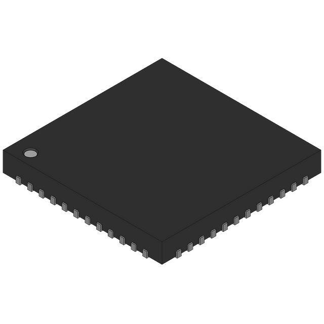


 工商网监
湘ICP备2023018690号
工商网监
湘ICP备2023018690号
