TLE4205G
1-A DC Motor Driver
Datasheet
Rev. 1.1, 2015-01-15
Automotive Power
�TLE4205G
1-A DC Motor Driver
Overview
Features
●
●
●
●
●
●
●
●
Max. driver current 1 A
Integrated free-wheeling diodes
Short-circuit proof to ground
Inhibit
ESD protected inputs
Temperature range – 40 °C ≤ Tj ≤ 150 °C
Green Product (RoHS compliant)
AEC Qualified
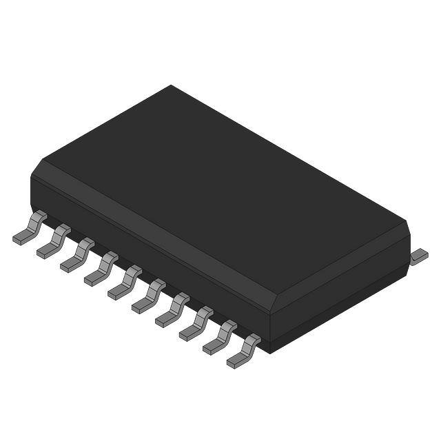
PG-DSO-20
Type
Marking
Package
TLE4205G
TLE4205G
PG-DSO-20
Description
TLE 4205G is an integrated power full-bridge DC-motor driver for a wide temperature
range, as required in automotive applications for example. The circuit contains two
power comparators that can be combined to a full-bridge circuit. For inductive loads
there are integrated free-wheeling diodes to + VS and ground. The outputs are shortcircuit proof up to 18 V supply voltage to ground and turn off when overtemperature
occurs. This IC is especially suitable for headlight-beam adjustment in automobiles.
Data Sheet
2
2015-01-19
�TLE4205G
Q2
N.C.
N.C.
GND
GND
GND
GND
- Ι2
+ Ι2
+Ι 1
1
2
3
4
5
6
7
8
9
10
20
19
18
17
16
15
14
13
12
11
VS
Q1
N.C.
GND
GND
GND
GND
N.C.
ΙNH
-Ι 1
AEP01318
Figure 1
Data Sheet
Pin Configuration (top view)
3
2015-01-19
�TLE4205G
Pin Definitions and Functions
Pin No. Symbol
Function
1
Q2
Output 2 of channel 2; push-pull B output with DC short-circuit
protection to ground. Integrated free-wheeling diodes to ground
and the supply voltage.
2
N.C.
Not connected
3
N.C.
Not connected
4-7
GND
Ground
8
– I2
Inverting input channel 2; to be wired according to general
rules.
9
+ I2
Non-inverting input channel 2; to be wired according to
general rules.
10
+ I1
Non-inverting input channel 1; see pin 9.
11
– I1
Inverting input channel 1; see pin 8.
12
INH
Inhibit; the IC is passive when this pin is open or connected to
ground.
13
N.C.
Not connected
14-17
GND
Ground
18
N.C.
Not connected
19
Q1
Output Q1 of channel 1, see pin 1.
20
VS
Supply voltage VS; must be blocked with a ceramic capacitor
of at least 100 nF directly on the pins of the IC.
Data Sheet
4
2015-01-19
�TLE4205G
VS
20
+I1
-I1
10
T1
∞
19 Q1
+
11
-
T2
Power Limiting for
T1, T3
Temperature
Protection
INH 12
+I2
9
-I2
8
T3
∞
1
+
-
Q2
T4
4-7
14-17
GND
Figure 2
Data Sheet
Block Diagram
5
2015-01-19
�TLE4205G
Circuit Description
The IC contains two amplifiers with typical open-loop gain of 80 dB at 500 Hz.
The input stages consist of PNP-differential amplifiers. This produces a common-mode
input range of 0 V to nearly VS and a maximum differential input voltage of VS. The IC is
guarded against ground shorts by an SOA-protective circuit. The output transistors are
turned off if the chip temperature exceeds approx. 160 °C. The IC can be turned off by
an inhibit input, which very much reduces current consumption.
VS
+I2
10 kΩ
10 kΩ
Q1
Q2
-I2
-I1
+I1
10 kΩ
30 kΩ
10 kΩ
10 kΩ
INH
Figure 3
Data Sheet
200
kΩ
GND
Circuit Diagram
6
2015-01-19
�TLE4205G
Absolute Maximum Ratings
Tj = − 40 to 150 °C
Parameter
Symbol
min.
max.
Supply voltage
VS
VID
IQ
IS
IGND
VI
VInh
Tj
Tstg
– 0.3
45
V
–
–
± VS
V
ΔV8-9 or ΔV10-11
Differential input voltage
Output current
Limit Values
Unit Remarks
–1
1
A
–
2.5
3
A
–
–3
2.5
A
I2
– 15
VS
VS
V
V
V8; V9; V10; V11
V12
–
150
°C
–
– 50
150
°C
–
6
32
V
–
Case temperature
VS
TC
– 40
95
°C
PDmax = 3 W
Thermal resistance
junction - ambient
junction - case
Rth JA
Rth JC
–
–
65
20
K/W
K/W
Supply current
Ground current
Input voltage
Inhibit input
Junction temperature
Storage temperature
– 15
Operating Range
Supply voltage
Outputs pin 1 and pin 19 short-circuit proof to GND at VS ≤ 18 V
Characteristics
6 V < VS < 18 V; – 40 °C < Tj < 150 °C
Parameter
Symbol
Limit Values
min.
typ.
max.
Unit
Test Condition
General
Open-circuit
current consumption
IS
–
10
30
mA
active, both outputs
high
Open-circuit
current consumption
IS
–
10
100
μA
inhibit
Turn-ON dead time
ref. to V12 OFF/ON
td ON
–
10
20
μs
|I1,19| < 1 A
Turn-OFF dead time
ref. to V12 OFF/ON
td OFF
–
10
20
μs
|I1,19| < 1 A
Data Sheet
7
2015-01-19
�TLE4205G
Characteristics (cont’d)
6 V < VS < 18 V; – 40 °C < Tj < 150 °C
Parameter
Symbol
Limit Values
Unit
Test Condition
min.
typ.
max.
Open-loop gain
GVO
50
80
–
dB
f = 500 Hz
VIO
ΔVIO/ΔT
IIO
II
ΔII/ΔT
VIC
– 7.5
–
7.5
mV
RS = 10 kΩ;
–
20
30
μV/K
–
– 75
–
75
mA
–
– 300
–
300
nA
–
–
–
5
nA/K
–
–
–
VS – 2 V
–
Input common-mode
range, negative
VIC
–
–
– 0.5
V
–
Power-supply
rejection ratio
PSSR
–
–
200
μV/V
RS = 10 kΩ;
Common-mode
rejection ratio
CMRR
70
80
–
dB
–
Inputs
Input zero voltage
Input-voltage drift
Input zero current
Input current
Input-current drift
Input common-mode
range, positive
Data Sheet
8
2015-01-19
�TLE4205G
Characteristics (cont’d)
6 V < VS < 18 V; – 40 °C < Tj < 150 °C
Parameter
Symbol
Limit Values
Unit
Test Condition
min.
typ.
max.
VSat U
VSat L
VFU
–
1.35
1.5
V
–
0.8
1.2
V
–
1
1.5
V
IQ = – 0.6 A
IQ = 0.6 A
IF = 0.6 A
Forward voltage of
free-wheeling diode
VFL
–
1
1.5
V
IF = 0.6 A
Slew rate of VQ
dVqdtr
–
0.5
–
V/μs
–
Switching threshold
high
VIH
2
–
–
V
–
Switching threshold
low
VIL
–
–
0.8
V
–
H-input current
IIH
IIH
–
100
–
μA
–
0
–
μA
V12 = 5 V
V12 = 0 V
Outputs
Saturation voltage
Saturation voltage
Forward voltage of
free-wheeling diode
Inhibit Input
L-input current
Note: VSat U = upper
VSat L = lower
Data Sheet
9
2015-01-19
�TLE4205G
IS
1000 µF
63V
470nF
VS
IINH
INH
I-I2
-I2
I+I2
+I2
I-I1
V12
V8
V9
V11
TLE4205G
RL
-I1
IQ2
I+I1
VS
IQ1
Q1
+I1
Q2
V10
VQ2
GND
VQ1
IGND
Figure 4
Test Circuit
100 nF
VINH
12
V+I1
10
V-I1
11
20
∞
+
AMP1
19
9
8
V-I2
VQ1 220 nF 1Ω
-
TLE4205G
V+I2
13.5V
100 µF*)
M
∞
+
AMP2
1
220 nF 1Ω
VQ2
-
4-7, 14-17
*)
Figure 5
Data Sheet
The value depends on load current and wiring inductivity
Application Circuit
10
2015-01-19
�TLE4205G
Forward Voltage of the Free-Wheeling
Diodes versus Junction Temperature
IED00955
1.6
V
VF
Start Point of the SOA-Protection
Circuit versus Junction Temperature
IED00956
2.4
Ι F = 0.6 A
A
1.4
I
2.0
VFU
1.2
1.6
VFL
1.0
V S = 13.5 V
0.8
1.2
0.6
0.8
0.4
0.4
0.2
0
-40
0
40
80
˚C
0
120
-40
0
Current Consumption versus
Junction Temperature
IED00957
1.6
V
IED00958
18
mA
16
I Q = 600 mA
VS = 13.5 V
1.4
120
TJ
Saturation Voltage versus Junction
Temperature
V Sat
80 ˚C
40
TJ
IS
VSat U
14
1.2
VS = 13.5 V
12
1.0
10
VSat L
0.8
8
0.6
6
0.4
4
0.2
2
0
-40
0
-40
0
40
80
˚C 120
40
80
˚C 120
TJ
TJ
Data Sheet
0
11
2015-01-19
�TLE4205G
2.65 MAX.
0.35 x 45˚
1.27
0.35 +0.15
0.1 20x
2)
0.2 20x
20
1
0.4 +0.8
0.23 +0.09
7.6 -0.2
1)
8˚ MAX.
2.45 -0.2
0.2 -0.1
Package Outlines
10.3 ±0.3
11
10
12.8 -0.2 1)
Index Marking
1) Does not include plastic or metal protrusion of 0.15 max. per side
2) Does not include dambar protrusion of 0.05 max. per side
Figure 6
PG-DSO-20 (Plastic Dual Small Outline)
Green Product (RoHS compliant)
To meet the world-wide customer requirements for environmentally friendly products
and to be compliant with government regulations the device is available as a green
product. Green products are RoHS-Compliant (i.e Pb-free finish on leads and suitable
for Pb-free soldering according to IPC/JEDEC J-STD-020).
You can find all of our packages, sorts of packing and others in our
Infineon Internet Page “Products”: http://www.infineon.com/products.
Dimensions in mm
Data Sheet
12
2015-01-19
�TLE4205G
Revision History
Revision
1.1
Data Sheet
Date
2015-01-19
Changes
Initial version of RoHS-compliant derivate of TLE 4205G
• Page 1: Added Coverpage,
• All pages: Infineon logo updated
• Page 2:
“added AEC qualified” and “RoHS” logo, “Green Product
(RoHS compliant)” and “AEC qualified” statement added
to feature list, package name changed to RoHS
compliant versions, package picture updated
• Page 12:
Package name changed to RoHS compliant versions,
“Green Product” description added
• Page 13: added Revision History
• Page 14: added Legal Disclaimer
• Page 7, Page 9: V9 designating the voltage at INH pin
renamed V12
13
2015-01-19
�Edition 2015-01-19
Published by
Infineon Technologies AG
81726 Munich, Germany
© 2015 Infineon Technologies AG
All Rights Reserved.
Legal Disclaimer
The information given in this document shall in no event be regarded as a guarantee of conditions or
characteristics. With respect to any examples or hints given herein, any typical values stated herein
and/or any information regarding the application of the device, Infineon Technologies hereby disclaims
any and all warranties and liabilities of any kind, including without limitation, warranties of noninfringement of intellectual property rights of any third party.
Information
For further information on technology, delivery terms and conditions and prices, please contact the nearest Infineon
Technologies Office (www.infineon.com).
Warnings
Due to technical requirements, components may contain dangerous substances. For information on the types in
question, please contact the nearest Infineon Technologies Office.
Infineon Technologies components may be used in life-support devices or systems only with the express written
approval of Infineon Technologies, if a failure of such components can reasonably be expected to cause the failure of
that life-support device or system or to affect the safety or effectiveness of that device or system. Life support devices
or systems are intended to be implanted in the human body or to support and/or maintain and sustain and/or protect
human life. If they fail, it is reasonable to assume that the health of the user or other persons may be endangered.
�
很抱歉,暂时无法提供与“TLE4205G”相匹配的价格&库存,您可以联系我们找货
免费人工找货- 国内价格
- 1+16.51320
- 10+13.93200
- 30+12.32280
- 100+10.67040