TLE4208G
Quad Half-Bridge Driver IC
Data Sheet
Rev. 1.4, 2016-02-02
Automotive Power
�TLE4208G
Table of Contents
Table of Contents
1
Overview . . . . . . . . . . . . . . . . . . . . . . . . . . . . . . . . . . . . . . . . . . . . . . . . . . . . . . . . . . . . . . . . . . . . . . . 3
2
Block Diagram . . . . . . . . . . . . . . . . . . . . . . . . . . . . . . . . . . . . . . . . . . . . . . . . . . . . . . . . . . . . . . . . . . . 4
3
3.1
3.2
Pin Configuration . . . . . . . . . . . . . . . . . . . . . . . . . . . . . . . . . . . . . . . . . . . . . . . . . . . . . . . . . . . . . . . . 6
Pin Assignment . . . . . . . . . . . . . . . . . . . . . . . . . . . . . . . . . . . . . . . . . . . . . . . . . . . . . . . . . . . . . . . . . . . 6
Pin Definitions and Functions . . . . . . . . . . . . . . . . . . . . . . . . . . . . . . . . . . . . . . . . . . . . . . . . . . . . . . . . 6
4
4.1
4.2
4.3
4.3.1
General Product Characteristics . . . . . . . . . . . . . . . . . . . . . . . . . . . . . . . . . . . . . . . . . . . . . . . . . . . . 8
Absolute Maximum Ratings . . . . . . . . . . . . . . . . . . . . . . . . . . . . . . . . . . . . . . . . . . . . . . . . . . . . . . . . . 8
Functional Range . . . . . . . . . . . . . . . . . . . . . . . . . . . . . . . . . . . . . . . . . . . . . . . . . . . . . . . . . . . . . . . . . 9
General Electrical Characteristics . . . . . . . . . . . . . . . . . . . . . . . . . . . . . . . . . . . . . . . . . . . . . . . . . . . . 10
Electrical Characteristics . . . . . . . . . . . . . . . . . . . . . . . . . . . . . . . . . . . . . . . . . . . . . . . . . . . . . . . . . 10
5
Application Information . . . . . . . . . . . . . . . . . . . . . . . . . . . . . . . . . . . . . . . . . . . . . . . . . . . . . . . . . . 12
6
Package Outlines . . . . . . . . . . . . . . . . . . . . . . . . . . . . . . . . . . . . . . . . . . . . . . . . . . . . . . . . . . . . . . . 14
7
Revision History . . . . . . . . . . . . . . . . . . . . . . . . . . . . . . . . . . . . . . . . . . . . . . . . . . . . . . . . . . . . . . . . 15
Data Sheet
2
Rev. 1.4, 2016-02-02
�1-A Quad Half-Bridge Driver IC
1
TLE4208G
Overview
Features
•
•
•
•
•
•
•
•
•
•
•
•
•
•
•
•
Driver for up to 3 motors
Delivers up to 0.8 A continuous
Optimized for DC motor management applications
Very low current consumption in stand-by (Inhibit) mode
Low saturation voltage; typ.1.2 V total @ 25 °C; 0.4 A
Output protected against short circuit
Error flag diagnosis
Overvoltage lockout and diagnosis
Undervoltage lockout
CMOS/TTL compatible inputs with hysteresis
No crossover current
Internal clamp diodes
Overtemperature protection with hysteresis and diagnosis
Enhanced power DSO-Package
Green Product (RoHS compliant)
AEC Qualified
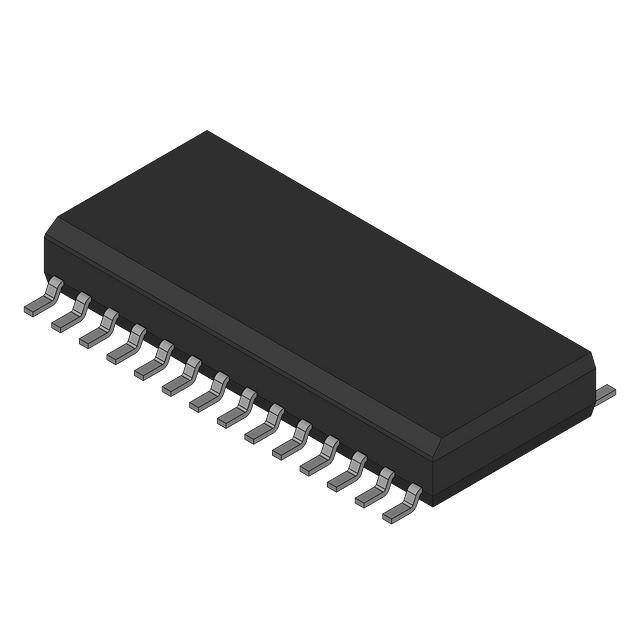
PG-DSO-28
Description
The TLE4208G is a protected Quad-Half-Bridge-Driver designed specially for automotive and industrial motion
control applications. The part is built using Infineons bipolar high voltage power technology DOPL.
In a cascade configuration up to three actuators (DC motors) can be connected between the four half-bridges.
These four half-bridges are configured as 2 dual-half-bridges, which are supplied and controlled separately.
Operation modes forward (cw), reverse (ccw), brake and high impedance are invoked from a standard interface.
The standard enhanced power PG-DSO-28 package meets the application requirements and saves PCB-board
space and costs. Moreover the package is RoHS compliant.
Furthermore the built-in features like diagnosis, over- and undervoltage-lockout, short-circuit protection, overtemperature protection and the very low quiescent current in stand-by mode will open a wide range of automotive
and industrial applications.
Type
Package
Marking
TLE4208G
PG-DSO-28
TLE4208G
Data Sheet
3
Rev. 1.4, 2016-02-02
�TLE4208G
Block Diagram
2
Block Diagram
TLE 4208 G
INH 12
27
25
V S12
Inhibit 1,2
DRV1
EF 12
IN1
IN2
2
3
26
5
Fault-Detection 1,2
INH 12
0
1
1
1
1
IN1
IN2
OUT1
OUT2
X
0
0
1
1
X
0
1
0
1
Z
L
L
H
H
Z
L
H
L
H
OUT1
DRV2
24
OUT2
1,6,7,8,
9,14,
GND
INH 34
13
20,21,
22,23
Inhibit 3,4
DRV3
EF 34
IN3
IN4
16
12
17
10
Fault-Detection 3,4
INH 34
0
1
1
1
1
IN3
IN4
OUT3
OUT4
X
0
0
1
1
X
0
1
0
1
Z
L
L
H
H
Z
L
H
L
H
OUT3
DRV4
19
18
OUT4
V S34
AEB02350
Figure 1
Block Diagram
Input Logic
Table 1
Functional Truth Table of Halfbridge 1 and 2
INH12
IN1
IN2
OUT1
OUT2
MODE
0
X
X
Z
Z
Stand-by
1
0
0
L
L
Brake LL
1
0
1
L
H
CW
1
1
0
H
L
CCW
1
1
1
H
H
Brake HH
Note: Half-Bridge 1 and 2 connected to a full-bridge
Data Sheet
4
Rev. 1.4, 2016-02-02
�TLE4208G
Block Diagram
Table 2
Functinal Truth Table of Halfbridge 3 and 4
INH34
IN3
IN4
OUT3
OUT4
MODE
0
X
X
Z
Z
Stand-by
1
0
0
L
L
Brake LL
1
0
1
L
H
CW
1
1
0
H
L
CCW
1
1
1
H
H
Brake HH
IN:
0 = Logic LOW
1 = Logic HIGH
X = Don’t Care
OUT:
Z = Output in tristate condition
L = Output in sink condition
X = Output in source condition
Note: Half-Bridge 3 and 4 connected to a full-bridge
Table 3
Diagnosis
EF12
EF34
Error
1
1
no error
0
1
over temperature of half-bridge 1 and 2 OR
0
1
over voltage of half-bridge 1 and 2
1
0
over temperature of half-bridge 3 and 4 OR
1
0
over voltage of half-bridge 3 and 4
0
0
over temperature of all half-bridges OR
0
0
over voltage of all half-bridge
Data Sheet
5
Rev. 1.4, 2016-02-02
�TLE4208G
Pin Configuration
3
Pin Configuration
3.1
Pin Assignment
GND
EF12
IN1
N.C.
OUT1
GND
GND
GND
GND
OUT3
N.C.
IN3
INH 34
GND
1
2
3
4
5
6
7
TLE 4208 G
8
9
10
11
12
13
14
28
27
26
25
24
23
22
21
20
19
18
17
16
15
N.C.
INH12
IN2
V S12
OUT2
GND
GND
GND
GND
OUT4
V S34
IN4
EF 34
N.C.
AEP02349
Figure 2
Pin Configuration
3.2
Pin Definitions and Functions
Pin
Symbol
Function
1, 6, 7, GND
8, 9, 14,
20, 21,
22, 23
Ground; negative reference potential for blocking capacitor
2
EF12
Error Flag output of half-bridges 1 and 2;
open collector; low = error
3
IN1
Input channel of half-bridge 1;
controls OUT 1
4, 11,
15, 28
N.C.
Not Connected
5
OUT 1
Power output of half-bridge 1; short circuit protected; with integrated clamp
diodes
10
OUT 3
Power output of half-bridge 3; short circuit protected; with integrated clamp
diodes
12
IN3
Input channel of half-bridge 3;
controls OUT 3
13
INH34
Inhibit input of half-bridges 3 and 4;
low = half-bridges 3 and 4 in stand-by
Data Sheet
6
Rev. 1.4, 2016-02-02
�TLE4208G
Pin Configuration
Pin
Symbol
Function
16
EF34
Error Flag output of half-bridges 3 and 4;
open collector; low = error
17
IN4
Input channel of half-bridge 4;
controls OUT 4
18
VS34
Power supply voltage of half-bridges 3 and 4;
positive reference potential for blocking capacitor
19
OUT 4
Power output of half-bridge 4; short circuit protected; with integrated clamp diodes
24
OUT 2
Power-output of half-bridge 2;
short circuit protected; with integrated clamp diodes
25
VS12
Power supply voltage of half-bridges 1 and 2;
positive reference potential for blocking capacitor
26
IN4
Input channel of half-bridge 4;
controls OUT 2
27
INH12
Inhibit input of half-bridges 1 and 2;
low = half-bridges 1 and 2in stand-by
Data Sheet
7
Rev. 1.4, 2016-02-02
�TLE4208G
General Product Characteristics
4
General Product Characteristics
4.1
Absolute Maximum Ratings
Table 4
Absolute Maximum Ratings
Tj = -40°C to +150°; all voltages with respect to ground, positive current flowing into pin
(unless otherwise specified)
Parameter
Symbol
Values
Unit
Note /
Test Condition
–
Min.
Typ.
Max.
VS12, VS34
VS12, VS34
-0.3
–
45
V
-1
–
–
V
t < 0.5s;
Logic input voltages
(IN1; IN2; INH12;
IN3; IN4; INH34)
VI
-5
V
IS12, IS34 > -2A
0V < VS12, VS34 <
Logic output voltage
(EF12; EF34)
VEF12, VEF34
–0.3
–
20
V
0V < VS12, VS34 <
45V
IOUT1-4
IOUT1-4
IOUT1-4
IEF12-34
–
–
–
A
internally limited
–
–
–
A
internally limited
-1
–
1
A
–
-2
–
5
mA
–
Tj
Tstg
-40
–
150
°C
–
-50
–
150
°C
–
Rthj-pin
RthjA
–
–
25
K/W
measured to pin 7
–
–
65
kV
–
Voltages
Supply Voltage
Supply Voltage
–
20
45V
Currents
Output Current (cont.)
Output Current (peak)
Output Current (diode)
Output Current (EF)
Temperatures
Junction Temperature
Storage Temperature
Thermal Resistances
Junction pin
Junction ambient
Notes
1. Stresses above the ones listed here may cause permanent damage to the device. Exposure to absolute
maximum rating conditions for extended periods may affect device reliability.
2. Integrated protection functions are designed to prevent IC destruction under fault conditions described in the
data sheet. Fault conditions are considered as “outside” normal operating range. Protection functions are not
designed for continuous repetitive operation.
Data Sheet
8
Rev. 1.4, 2016-02-02
�TLE4208G
General Product Characteristics
4.2
Functional Range
Table 5
Functional Range
Parameter
Symbol
Values
Unit
Note /
Test Condition
Min.
Typ.
Max.
Supply Voltage
VS12,VS34
VUV_OFF
–
18
V
After VS12,VS34 rising
above VUV_ON
Extended Supply Voltage
Range for Operation
VS12,VS34
-0.3
–
VUV_ON
V
Outputs in tristate
Supply Voltage transients
slew rate
VS12,VS34
-0.3
–
VUV_OFF
V/µs
Outputs in tristate
Logic input voltages
(IN1; IN2; INH12;
IN3; IN4; INH34)
VI
-2
–
18
V
–
Junction Temperature
Tj
-40
–
150
°C
–
Note: Within the functional or operating range, the IC operates as described in the circuit description. The electrical
characteristics are specified within the conditions given in the Electrical Characteristics table.
Data Sheet
9
Rev. 1.4, 2016-02-02
�TLE4208G
General Product Characteristics
4.3
General Electrical Characteristics
4.3.1
Electrical Characteristics
Table 6
Electrical Characteristics
VS12 =VS34 =8 V to 18 V, INH12 = INH34 = HIGH; IOUT1-4 = 0A; Tj = -40°C to +150°, all voltages with respect to ground,
positive current flowing into pin (unless otherwise specified)
Parameter
Symbol
Values
Unit
Note /
Test Condition
IS = IS12 + IS34
IS = IS12 + IS34;
VS12 = VS34 = 13.2V;
Tj = 25 °C
Min.
Typ.
Max.
–
–
100
µA
–
20
40
µA
Current Consumption
INH12 = INH34 = LOW
Quiescent current
Quiescent current
IS
IS
INH12 = HIGH and INH34 = LOW or INH12 = LOW and INH34 = HIGH
–
10
20
mA
–
Supply current
IS12, IS34
IS12, IS34
–
–
30
mA
Supply current
IS12, IS34
–
–
50
mA
IOUT1/3 = 0.4A
IOUT2/4 = -0.4A
IOUT1/3 = 0.8A
IOUT2/4 = -0.8A
VUV ON
VUV_OFF
VUV_HY
VOV OFF
VOV_ON
VOV_HY
–
6.5
7.5
V
5
6
–
V
–
0.5
–
V
–
20
24
V
18
19.5
–
V
–
0.5
–
V
VS12,VS34 increasing
VS12,VS34 decreasing
VUV ON - VUV OFF
VS12,VS34 increasing
VS12,VS34 decreasing
VOV OFF - VOV ON
Supply current
Over- and Under Voltage Lockout
UV Switch ON voltage
UV Switch OFF voltage
UV ON/ OFF hysteresis
OV Switch OFF voltage
OV Switch ON voltage
OV ON/ OFF hysteresis
Outputs OUT1; OUT2; OUT3; OUT4
Saturation Voltages
Source (upper)
IOUT12, IOUT34 = – 0.2 A
VSAT_U
–
0.85
1.15
V
Tj= 25°C
Source (upper)
IOUT12, IOUT34 = – 0.4 A
VSAT_U
–
0.90
1.20
V
Tj= 25°C
Sink (upper)
IOUT12, IOUT34 = – 0.8 A
VSAT_U
–
1.10
1.50
V
Tj= 25°C
Sink (lower)
IOUT12, IOUT34 = 0.2 A
VSAT_L
–
0.15
0.23
V
Tj= 25°C
Sink (lower)
IOUT12, IOUT34 = 0.4 A
VSAT_L
–
0.25
0.40
V
Tj= 25°C
Sink (lower)
IOUT12, IOUT34 = 0.8 A
VSAT_L
–
0.45
0.75
V
Tj= 25°C
Total Drop
IOUT12, IOUT34 = 0.2 A
VSAT
–
1
1.4
V
VSAT = VSAT_U+VSAT_L
Data Sheet
10
Rev. 1.4, 2016-02-02
�TLE4208G
General Product Characteristics
Table 6
Electrical Characteristics
VS12 =VS34 =8 V to 18 V, INH12 = INH34 = HIGH; IOUT1-4 = 0A; Tj = -40°C to +150°, all voltages with respect to ground,
positive current flowing into pin (unless otherwise specified)
Parameter
Symbol
Values
Min.
Typ.
Max.
Unit
Note /
Test Condition
Total Drop
IOUT12, IOUT34 = 0.4 A
VSAT
–
1.2
1.7
V
VSAT = VSAT_U+VSAT_L
Total Drop
IOUT12, IOUT34 = 0.8 A
VSAT
–
1.6
2.5
V
VSAT = VSAT_U+VSAT_L
VFU
ILKU
VFL
–
1
1.5
V
–
–
5
mA
–
0.9
1.4
V
IF = 0.4A
IF = 0.4A1)
IF = 0.4A
VIH
VIL
VIHY
IIH
IIL
–
2.0
3.0
V
–
1.0
1.5
–
V
–
–
0.5
–
V
–
-2
–
10
µA
-100
-20
-5
µA
VI = 5V
VI = 0V
VIH
VIL
VIHY
IIH
IIL
–
2.7
3.5
V
–
1.0
2.0
–
V
–
–
0.7
–
V
–
–
100
250
µA
-10
–
10
µA
VINH = 5V
VINH = 0V
VEFL
IEFLK
–
0.2
0.4
V
IEF = 2 mA
–
–
10
µA
0V < VEF < 7V
Thermal shutdown junction
temperature
TjSD
150
175
200
°C
–
Thermal switch-on junction
temperature
TjSO
120
–
170
°C
–
Temperature hysteresis
∆T
–
30
–
K
–
Clamp Diodes
Forward voltage; upper
Upper leakage current
Forward voltage; lower
Input Interface
Logic Inputs IN1; IN2; IN3; IN4
H-input voltage
L-input voltage
Hysteresis of input voltage
H-input current
L-input current
Logic Inputs INH12; INH34
H-input voltage
L-input voltage
Hysteresis of input voltage
H-input current
L-input current
Error Flags EF12; EF34
L-output voltage level
Leakage current
Thermal Shutdown
1) Not subject to production test, specified by design
Data Sheet
11
Rev. 1.4, 2016-02-02
�TLE4208G
Application Information
5
Application Information
Note: The following information is given as a hint for the implementation of the device only and shall not be
regarded as a description or warranty of a certain functionality, condition or quality of the device.
Watchdog In
Watchdog Out
Reset Out
1
WDO WDI
R
V CC
TLE 4278 G
2
14
Q
R QA
10 k Ω
13
8
9
D1
1N4001
Watchdog
Adjust
6 3,4,5,10,11,12 7
D
R QB
10 k Ω
VS = 12 V
Input
GND
Reset
Adjust
CD
100 nF
CQ
22 μF
R WA
100 k Ω
TLE 4208 G
INH12 27
CΙ
CS
100 nF 22 μF
26 V S12
Inhibit 1,2
DRV1
EF12 2
IN1 3
IN2 26
μC
5 OUT1
Fault-Detection 1,2
INH12
0
1
1
1
1
IN1 IN2 OUT1 OUT2
X
0
0
1
1
INH34 13
X
0
1
0
1
Z
L
L
H
H
24
Z
L
H
L
H
OUT2
1,6,7,
8,9,14
Inhibit 3,4
DRV3
EF34 16
IN3 12
IN4 17
IN3
0
1
1
1
1
X
0
0
1
1
IN4 OUT3 OUT4
X
0
1
0
1
Z
L
L
H
H
GND
20,21,
22,23
10 OUT3
Fault-Detection 3,4
INH34
M1
DRV2
M2
DRV4
Z
L
H
L
H
19
OUT4
18 V S34
AES02351
Figure 3
Application Circuit 1 (Device is used as Dual-Full-Bridge-Driver)
Note: This is a very simplified example of an application circuit. The function must be verified in the real application.
Data Sheet
12
Rev. 1.4, 2016-02-02
�TLE4208G
Application Information
Diagrams
Quiescent current IS over Temperature
Saturation Voltage of Source VSAT U over Temperature
AED02352
50
AED02308
1500
V SAT U
μA
VS = 14 V
1250
Ι S 40
Ι OUT = 800 mA
mV
30
1000
Ι OUT = 400 mA
750
Ι OUT = 200 mA
VS = 18 V
VS = 13.2 V
20
500
VS = 8 V
10
250
0
-50
0
50
0
-50
100 C 150
Tj
50
100 ˚C 150
Tj
Total Drop at outputs VSAT over Temperature
Saturation Voltage of Sink VSAT L over Temperature
1000
V SAT L
0
AED02310
2000
AED02309
V SAT
VS = 14 V
VS = 14 V
mV
mV
Ι OUT = 800 mA
1500
750
Ι OUT = 400 mA
Ι OUT = 800 mA
500
Ι OUT = 200 mA
1000
Ι OUT = 400 mA
500
250
Ι OUT = 200 mA
0
-50
0
50
0
-50
100 ˚C 150
Tj
Data Sheet
0
50
100 ˚C 150
Tj
13
Rev. 1.4, 2016-02-02
�TLE4208G
Package Outlines
1.27
0.1
0.35 +0.15 2)
1
8˚ MAX.
7.6 -0.2 1)
0.4 +0.8
10.3 ±0.3
0.2 28x
28
0.35 x 45˚
0.23 +0.09
2.65 MAX.
2.45 -0.2
Package Outlines
0.2 -0.1
6
15
18.1 -0.4
1)
14
Index Marking
1)
2)
Figure 4
Does not include plastic or metal protrusion of 0.15 max. per side
Does not include dambar protrusion of 0.05 max. per side
PG-DSO-28
Green Product (RoHS compliant)
To meet the world-wide customer requirements for environmentally friendly products and to be compliant with
government regulations the device is available as a green product. Green products are RoHS-Compliant (i.e Pbfree finish on leads and suitable for Pb-free soldering according to IPC/JEDEC J-STD-020).
For further information on alternative packages, please visit our website:
http://www.infineon.com/packages.
Data Sheet
14
Dimensions in mm
Rev. 1.4, 2016-02-02
�TLE4208G
Revision History
7
Revision History
Revision
Date
Changes
Rev. 1.4
2016-02-02
Correction of typographical errors
Page 10: VOFF_OFF and VOFF_ON are inverted. No change of the device
behavior.
Page 10,11: VS1, respectively VS2, renamed VS12 and VS34
Rev. 1.3
2014-02-12
Updated package designation and to latest data sheet formatting
Rev. 1.2
2011-04-11
Updated package designation to reflect various production sites.
Rev. 1.1
2008-02-04
Initial version of RoHS-compliant derivate of TLE4208G
Page 1: added AEC certified statement
Page 1 and 13: added RoHS compliance statement and Green product feature
Page 1 and 3: Editorial change: deleted "fully" (The term "fully protected" often
leads to misunderstandings as it is unclear with respect to which parameters).
Page 1 and 14: Package changed to RoHS compliant version
Page 15: added Revision History, updated Legal Disclaimer
Data Sheet
15
Rev. 1.4, 2016-02-02
�Edition 2016-02-02
Published by
Infineon Technologies AG
81726 Munich, Germany
© 2016 Infineon Technologies AG
All Rights Reserved.
Legal Disclaimer
The information given in this document shall in no event be regarded as a guarantee of conditions or
characteristics. With respect to any examples or hints given herein, any typical values stated herein and/or any
information regarding the application of the device, Infineon Technologies hereby disclaims any and all warranties
and liabilities of any kind, including without limitation, warranties of non-infringement of intellectual property rights
of any third party.
Information
For further information on technology, delivery terms and conditions and prices, please contact the nearest
Infineon Technologies Office (www.infineon.com).
Warnings
Due to technical requirements, components may contain dangerous substances. For information on the types in
question, please contact the nearest Infineon Technologies Office.
Infineon Technologies components may be used in life-support devices or systems only with the express written
approval of Infineon Technologies, if a failure of such components can reasonably be expected to cause the failure
of that life-support device or system or to affect the safety or effectiveness of that device or system. Life support
devices or systems are intended to be implanted in the human body or to support and/or maintain and sustain
and/or protect human life. If they fail, it is reasonable to assume that the health of the user or other persons may
be endangered.
�