Infineon® LITIX™ Linear
1 Channel High Side Current Source up to 500mA
TLE4242EJ
Infineon® LITIX™ Linear
1 Channel High Side Current Source up to 500mA
Datasheet
Rev. 1.10
2018-05-22
Automotive Power
�Infineon® LITIX™ Linear
TLE4242EJ
Table of Contents
Table of Contents
Table of Contents . . . . . . . . . . . . . . . . . . . . . . . . . . . . . . . . . . . . . . . . . . . . . . . . . . . . . . . . . . . . . . . . . 2
1
Overview . . . . . . . . . . . . . . . . . . . . . . . . . . . . . . . . . . . . . . . . . . . . . . . . . . . . . . . . . . . . . . . . . . . . . . . . 3
2
Block Diagram . . . . . . . . . . . . . . . . . . . . . . . . . . . . . . . . . . . . . . . . . . . . . . . . . . . . . . . . . . . . . . . . . . . 4
3
3.1
3.2
Pin Configuration . . . . . . . . . . . . . . . . . . . . . . . . . . . . . . . . . . . . . . . . . . . . . . . . . . . . . . . . . . . . . . . . . 5
Pin Assignment . . . . . . . . . . . . . . . . . . . . . . . . . . . . . . . . . . . . . . . . . . . . . . . . . . . . . . . . . . . . . . . . . . . . . . . . . . . 5
Pin Definitions and Functions . . . . . . . . . . . . . . . . . . . . . . . . . . . . . . . . . . . . . . . . . . . . . . . . . . . . . . . . . . . . . . 5
4
4.1
4.2
4.3
General Product Characteristics . . . . . . . . . . . . . . . . . . . . . . . . . . . . . . . . . . . . . . . . . . . . . . . . . . . .
Absolute Maximum Ratings . . . . . . . . . . . . . . . . . . . . . . . . . . . . . . . . . . . . . . . . . . . . . . . . . . . . . . . . . . . . . . . .
Functional Range . . . . . . . . . . . . . . . . . . . . . . . . . . . . . . . . . . . . . . . . . . . . . . . . . . . . . . . . . . . . . . . . . . . . . . . . .
Thermal Resistance . . . . . . . . . . . . . . . . . . . . . . . . . . . . . . . . . . . . . . . . . . . . . . . . . . . . . . . . . . . . . . . . . . . . . . .
5
5.1
5.2
5.3
5.3.1
Product Description . . . . . . . . . . . . . . . . . . . . . . . . . . . . . . . . . . . . . . . . . . . . . . . . . . . . . . . . . . . . . . 8
Output Current Setting . . . . . . . . . . . . . . . . . . . . . . . . . . . . . . . . . . . . . . . . . . . . . . . . . . . . . . . . . . . . . . . . . . . . 8
Protection Functions . . . . . . . . . . . . . . . . . . . . . . . . . . . . . . . . . . . . . . . . . . . . . . . . . . . . . . . . . . . . . . . . . . . . . . 9
Electrical Characteristics . . . . . . . . . . . . . . . . . . . . . . . . . . . . . . . . . . . . . . . . . . . . . . . . . . . . . . . . . . . . . . . . . 10
Typical Performance Characteristics . . . . . . . . . . . . . . . . . . . . . . . . . . . . . . . . . . . . . . . . . . . . . . . . . . . . . 12
6
6.1
Application Information . . . . . . . . . . . . . . . . . . . . . . . . . . . . . . . . . . . . . . . . . . . . . . . . . . . . . . . . . . 14
Further Application Information . . . . . . . . . . . . . . . . . . . . . . . . . . . . . . . . . . . . . . . . . . . . . . . . . . . . . . . . . . 14
7
Package Outlines . . . . . . . . . . . . . . . . . . . . . . . . . . . . . . . . . . . . . . . . . . . . . . . . . . . . . . . . . . . . . . . . 15
Datasheet
2
6
6
7
7
Rev. 1.10 2018-05-22
�TLE4242EJ
1
Infineon® LITIX™ Linear
Overview
Features
•
Adjustable constant current up to 500 mA
•
Wide input voltage range up to 42 V
•
Low drop voltage
•
Open load detection
•
Over temperature protection
•
Over load protection
•
Integrated reverse polarity protection
•
Wide temperature range -40 °C to 150 °C
•
Green Product (RoHS compliant)
•
AEC Qualified
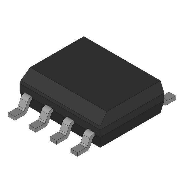
PG-DSO-8-27
Description
The TLE4242EJ is an integrated adjustable constant current source driving loads up to 500 mA. The output
current level can be adjusted via an external resistor. The IC is designed to supply high power LEDs under the
severe conditions of automotive applications resulting in constant brightness and extended LED lifetime. It is
provided in the surface mounted PG-DSO-8-27 package. Protection circuits prevent damage to the device in
case of over load, short circuit, reverse polarity and overheat. The connected LEDs are protected against
reverse polarity as well as over voltages up to 45 V.
The integrated PWM input of the TLE4242EJ permits LED brightness regulation by pulse width modulation.
Due to the high input impedance of the PWM input the LED driver can be operated as a protected high side
switch.
Table 1
Product Summary
Parameter
Symbol
Values
Operating voltage
VI(nom)
4.5 V … 42 V
Maximum output voltage
VQ(max)
40 V
Nominal output (load) current
IQ(nom)
135 mA
Minimum current limitation
IQ(lim,min)
476 mA
Current consumption in off mode
II(off,typ)
0.1 µA
Type
Package
Marking
TLE4242EJ
PG-DSO-8-27
TLE4242
Datasheet
3
Rev. 1.10, 2018-05-22
�Infineon® LITIX™ Linear
TLE4242EJ
Block Diagram
2
Block Diagram
I
PWM
6
8
1
Q
Bias Supp ly
4
Ban dgap
Reference
REF
Comparator
2
ST
Status
Delay
3
GND
Figure 2-1
Datasheet
5
D
AEB03500.VSD
Block Diagram
4
Rev. 1.10
2018-05-22
�Infineon® LITIX™ Linear
TLE4242EJ
Pin Configuration
3
Pin Configuration
3.1
Pin Assignment
(top view)
PWM
ST
GND
REF
Figure 3-1
3.2
1
8
2
9
3 GND
7
4
5
6
I
n.c.
Q
D
Pin Configuration
Pin Definitions and Functions
Pin
Symbol
Input/
Output
Function
1
PWM
I
Pulse Width Modulation Input; if not required, connect to I-pin1)
2
ST
O
Status Output; open collector output, connect to external pull-up resistor
3
GND
–
2)
4
REF
I
Reference Input; connect to shunt resistor
5
D
O
Status Delay; optional, connect to GND via an optional capacitor to extend
the status reaction time. Leave open, if no delay is required.
6
Q
O
Output
8
I
I
Input; battery supply, connect a decoupling ceramic capacitor of at least
100 nF directly at the IC to ground
9
GND
–
2)
Ground
Exposed Pad; connect to GND in application
1) Please take care of different maximum ratings of I- and PWM-pins during circuit design.
2) Connect all GND-pins together.
Datasheet
5
Rev. 1.10
2018-05-22
�Infineon® LITIX™ Linear
TLE4242EJ
General Product Characteristics
4
General Product Characteristics
4.1
Absolute Maximum Ratings
Table 4-1
Absolute Maximum Ratings1)
Tj = -40°C to +150°C; all voltages with respect to ground, positive current flowing into pin for input pins,
positive currents flowing out of pin for output pins (unless otherwise specified)
Parameter
Symbol
Values
Min.
Typ.
Max.
Unit
Note or
Test Condition
Number
Voltages
Input voltage
VI
-42
–
45
V
–
P_4.1.1
Output voltage
VQ
-1
–
40
V
–
P_4.1.2
Status output voltage
VST
-0.3
–
40
V
–
P_4.1.3
Status delay voltage
VD
-0.3
–
7
V
–
P_4.1.4
Reference input voltage
VREF
-1
–
16
V
–
P_4.1.5
PWM input voltage
VPWM
-40
–
40
V
–
P_4.1.6
Input current
II
–
–
–
A
internally limited P_4.1.7
Output current
IQ
–
–
–
A
internally limited P_4.1.8
Status output current
IST
-5
–
5
mA
–
P_4.1.9
Status delay current
ID
-1
–
1
mA
in off-state
10 min
P_4.1.17
Reference input current
IREF
-2
–
2
mA
–
P_4.1.10
PWM input current
IPWM
-1
–
1
mA
–
P_4.1.11
Junction Temperature
Tj
-40
–
150
°C
–
P_4.1.12
Storage Temperature
Tstg
-55
–
150
°C
–
P_4.1.13
VESD
-2
–
2
kV
HBM2)
P_4.1.14
3)
P_4.1.15
3)
P_4.1.16
Currents
Temperatures
ESD Susceptibility
ESD Susceptibility
ESD Susceptibility
VESD
ESD Susceptibility Pin 1, 4, 5, 8 VESD1,4,5,8
(corner pins) to GND
-500
-750
–
–
500
750
V
V
CDM
CDM
1) Not subject to production test, specified by design.
2) ESD susceptibility, HBM according to ANSI/ESDA/JEDEC JS001 (1.5k Ω, 100 pF)
3) ESD susceptibility, Charged Device Model “CDM” ESDA STM5.3.1 or ANSI/ESD S.5.3.1
Datasheet
6
Rev. 1.10
2018-05-22
�Infineon® LITIX™ Linear
TLE4242EJ
General Product Characteristics
Notes
1. Stresses above the ones listed here may cause permanent damage to the device. Exposure to absolute
maximum rating conditions for extended periods may affect device reliability.
2. Integrated protection functions are designed to prevent IC destruction under fault conditions described in the
data sheet. Fault conditions are considered as “outside” normal operating range. Protection functions are
not designed for continuous repetitive operation.
4.2
Functional Range
Table 4-2
Functional Range
Parameter
Symbol
Values
Min.
Typ.
Max.
Unit
Note or
Test Condition
Number
Input voltage range
VI
4.5
–
42
V
–
P_4.1.1
Status output voltage
VST
–
–
16
V
–
P_4.1.3
Status delay capacitance
CD
0
–
2.2
µF
–
P_4.1.4
PWM voltage
VPWM
0
–
40
V
–
P_4.1.6
Reference resistor
RREF
0
–
1.8
Ω
–
P_4.1.10
Junction Temperature
Tj
-40
–
150
°C
–
P_4.1.12
Note: Within the functional or operating range, the IC operates as described in the circuit description. The
electrical characteristics are specified within the conditions given in the Electrical Characteristics table.
4.3
Thermal Resistance
Note: This thermal data was generated in accordance with JEDEC JESD51 standards. For more information, go
to www.jedec.org.
Table 4-3
Thermal Resistance
Parameter
Symbol
1)
Junction to Case
Junction to Ambient
RthJC
RthJA
Values
Min.
Typ.
Max.
–
8
10
–
39
–
Unit
Note or
Test Condition
Number
K/W
–
P_4.3.1
K/W
2)
Ta = 85 °C
P_4.3.2
1) Not subject to production test, specified by design.
2)
Specified RthJA value is according to Jedec JESD51-2,-5,-7 at natural convection on FR4 2s2p board; The Product
(Chip + Package) was simulated on a 76.2 × 114.3 × 1.5 mm board with 2 inner copper layers (2 × 70 mm Cu, 2 × 35 mm
Cu). Where applicable a thermal via array under the exposed pad contacted the first inner copper layer.
Datasheet
7
Rev. 1.10
2018-05-22
�Infineon® LITIX™ Linear
TLE4242EJ
Product Description
5
Product Description
The TLE4242EJ is an adjustable constant current source providing currents up to 500 mA. The product is
optimized for automotive applications, but is suitable for industrial applications as well, where high currents
are required.
5.1
Output Current Setting
An external shunt resistor in the ground path of the connected LEDs is used to sense the LED current. A
regulation loop regulates the voltage drop at the shunt resistor RREF on a constant level of typ. 175 mV.
Selecting the appropriate shunt resistance allows to adjust the desired constant current level. The typical
output current is calculated according to Equation (5.1).
V REF
I Q typ = ------------R REF
(5.1)
VREF is the reference voltage with a typical value of 175 mV, details at Reference voltage. The equation applies
in a range of 0.39 Ω ≤ RREF ≤ 1.8 Ω.
The output current is shown as a function of the reference resistance in Chapter 5.3.1. With the PWM input the
LED brightness can be regulated via duty cycle. Also PWM = 0 V sets the TLE4242EJ in sleep mode resulting in
a very low current consumption II(off) Current consumption at Input-pin during off-state. Due to the high
impedance of the PWM input the PWM pin can also be used as an enable input.
The application example in Figure 6-1 shows a typical application with the TLE4242EJ LED driver. The three
LEDs are driven with an adequate supply current adjusted by the resistor RREF. Thus brightness variations due
to forward voltage spread of the LEDs are prevented. The luminosity spread arising from the LED production
process can be compensated via software by an appropriate duty cycle applied to the PWM pin. Therefore,
selection of the LEDs to forward voltage as well as to luminosity classes can be spared. The minimum supply
voltage for the application is the sum of the LED forward voltages, the TLE4242EJ drop voltage Minimum drop
voltage Vdr = VI - VQ and the max. voltage drop at the shunt resistor RREF of VREF(max) according to Reference
voltage.
The status output of the LED driver (ST) detects an open load condition enabling to supervise correct LED
function. A LED failure is detected, if the voltage drop at the shunt resistor RREF falls below typ. 25 mV. In this
case the status output pin ST is set low after a delay time, which is adjustable via an optional capacitor
connected to the pin D.
The functionality of the status ST and PWM-pin as well as their timings are shown in Figure 5-1. The pull up
resistor value at the ST-pin is recommended with RST_pu ≥ 4.7 kΩ. The status delay can be adjusted via the
capacitor connected to the timing pin D. The delay time tST(HL) and tST(LH) scales linearly with the capacitance
CD:
CD
- 10ms
t ST HL typ = ------------
(5.2)
CD
- 10s
t ST LH typ = ------------
(5.3)
47nF
47nF
Datasheet
8
Rev. 1.10
2018-05-22
�Infineon® LITIX™ Linear
TLE4242EJ
Product Description
VI
Open
Load
t
VPWM
VPWM(H)
VPWM(L)
tPWM(on)
IQ
t
tPWM(off)
tST(H
VD
t
L)
VD(H) *
VD(L) *
t
VST
VST(L)
t
* Parameters for internal use
only
Figure 5-1
5.2
Function and Timing Diagram
Protection Functions
The TLE4242EJ provides embedded protection functions, which are designed to prevent IC destruction under
fault conditions described in the data sheet. Fault conditions are considered as “outside” normal operating
range. Protection functions are neither designed for continuous nor for repetitive operation.
The following protection functions are embedded:
•
Over temperature protection realized by over temperature switch off (see Figure 5-2)
•
Over load protection realized by output current limitation and over temperature protection
•
Integrated reverse polarity protection
Datasheet
9
Rev. 1.10
2018-05-22
�Infineon® LITIX™ Linear
TLE4242EJ
Product Description
IQ
IQ(n o m)
Tj
Tj( OT)
Figure 5-2
5.3
Table 5-1
Over Temperature Protection
Electrical Characteristics
Electrical Characteristics
Vl = 13.5 V, RREF = 0.47 Ω, VPWM = 5.0 V, Tj = -40°C to +150°C, all voltages with respect to ground, positive current
flowing into pin for input pins, positive currents flowing out of pin for output pins (unless otherwise specified)
Parameter
Symbol
Current consumption at Input- II(off)
pin during off-state
Values
Min.
Typ.
Max.
–
0.1
2
Unit
Note or
Test Condition
µA
1)
V
Number
Tj = 85 °CVPWM = 0.0 P_5.3.1
Iop(on)
–
12
22
mA
VQ = 6.6 V
P_5.3.2
Output current
IQ
350
373
395
mA
2)
P_5.3.3
Output current
IQ
165
175
185
mA
VQ - VREF = 6.6 V, RREF = P_5.3.4
1.0 Ω
Output current
IQ
425
451
476
mA
VQ - VREF = 6.6 V, RREF = P_5.3.5
0.39 Ω
Output current
IQ
357
384
410
mA
5.4 V ≤ (VQ - VREF) ≤ 7.8 P_5.3.6
V;9 V ≤ VI ≤ 16 V
Output current limit
IQ(lim)
476
600
–
mA
RREF = 0 Ω
P_5.3.7
Minimum drop voltage
Vdr = VI - VQ
Vdr
–
0.35
0.7
V
IQ = 300 mA
P_5.3.8
VPWM(H)
2.6
–
–
V
–
P_5.3.9
Operational current
consumption in on-state
Iop = II - IQ
Output
VQ- VREF = 6.6 V
PWM Input
PWM high level
Datasheet
10
Rev. 1.10
2018-05-22
�Infineon® LITIX™ Linear
TLE4242EJ
Product Description
Table 5-1
Electrical Characteristics (continued)
Vl = 13.5 V, RREF = 0.47 Ω, VPWM = 5.0 V, Tj = -40°C to +150°C, all voltages with respect to ground, positive current
flowing into pin for input pins, positive currents flowing out of pin for output pins (unless otherwise specified)
Parameter
Symbol
Values
Min.
Typ.
Max.
Unit
Note or
Test Condition
Number
PWM low level
VPWM(L)
–
–
0.7
V
–
P_5.3.10
PWM input current
high level
IPWM(H)
–
–
10
µA
VPWM = 5.0 V
P_5.3.11
PWM input current
low level
IPWM(L)
-1
–
1
µA
VPWM = 0.0 V
P_5.3.12
Turn on delay time
tPWM(on)
0
15
40
µs
70% of VREF/RREF,
see Figure 5-1
P_5.3.13
Turn off delay time
tPWM(off)
0
15
40
µs
30% of VREF/RREF,
see Figure 5-1
P_5.3.14
Reference voltage
VREF
165
175
185
mV
0.39 Ω ≤ RREF ≤ 1.0 Ω P_5.3.15
VQ - VREF = 6.6 V
Reference input current
IREF
-1
0.1
1
µA
VREF = 180 mV
P_5.3.16
Lower status switching
threshold
VIQ(L)
15
25
–
mV
–
P_5.3.17
Upper status switching
threshold
VIQ(H)
–
30
40
mV
–
P_5.3.18
Status low voltage
VST(L)
–
–
0.4
V
IST = 1.5 mA
P_5.3.19
Leakage current
IST(leak)
–
–
5
µA
VST = 5.0 V
P_5.3.20
tST(HL)
6
10
14
ms
1)
CD = 47 nFST H → L P_5.3.21
CD = 47 nFST L → H
Reference
Status Output
Status Delay
Status reaction delay
tST(LH)
–
10
20
µs
1)
Over temperature protection
threshold
Tj(OT)
150
–
–
°C
1)
P_5.3.23
Reverse output current
-IQ(rev)
–
–
2
µA
1)
P_5.3.27
Status release delay
P_5.3.22
Protection
VI = -16 V
Output load: LED
with break down
voltage < -0.6 V
1) Not subject to production test, specified by design
2) VQ - VREF equals the forward voltage sum of the connected LEDs, see Figure 6-1
Datasheet
11
Rev. 1.10
2018-05-22
�Infineon® LITIX™ Linear
TLE4242EJ
Product Description
5.3.1
Typical Performance Characteristics
Data below show the behavior of a typical device.
IQ=f(RREF)
700
600
IQ [mA]
500
400
300
200
100
0
0
Figure 5-3
0,5
1
RREF [Ω]
1,5
2
Output Current IQ versus Reference Resistor RREF with VQ = 6.6 V
IQ=f(VI)
180
IQ [mA]
175
170
165
160
0
5
10
15
20
VI [Ω]
25
30
35
40
Figure 5-4
Output Current IQ versus Supply Voltage VI with VQ - VREF = 6.6 V and RREF = 1 Ω
Datasheet
12
Rev. 1.10
2018-05-22
�Infineon® LITIX™ Linear
TLE4242EJ
Product Description
VREF [mV]
VREF=f(Tj)
190
188
186
184
182
180
178
176
174
172
170
-50
Figure 5-5
0
50
Tj [°C]
100
150
Reference Voltage VREF versus Junction Temperature Tj
IPWM=f(VPWM)
50
IPWM [µA]
40
30
20
10
0
0
5
10
15
20
VPWM [V]
25
30
35
40
Figure 5-6
PWM Pin Input Current IPWM versus PWM Voltage VPWM at Tj = 25°C and VI = 13.5 V
Datasheet
13
Rev. 1.10
2018-05-22
�Infineon® LITIX™ Linear
TLE4242EJ
Application Information
6
Application Information
Note: The following information is given as a hint for the implementation of the device only and shall not be
regarded as a description or warranty of a certain functionality, condition or quality of the device.
5V
10 k
VBAT
ST
PWM
I
Q