Triple Voltage Regulator
TLE 4471
Features
•
•
•
•
•
•
•
•
•
•
•
•
•
•
Triple Voltage Regulator
Output Voltage 5 V with 450 mA Current Capability
Two tracked Outputs for 50 mA and 100 mA
Enable Function for main and tracked Output(s)
Reset with adjustable Threshold
Undervoltage- and Power On-Reset
Watchdog
Independent Watchdog- and Reset delay
Wide Temperature Range
Overtemperature Protection
Overvoltage Protection
Reverse Polarity Proof
Green Product (RoHS compliant)
AEC Qualified
Functional Description
The TLE 4471 is a monolithic integrated very low-drop triple voltage regulator. The main
output supplies loads up to 450 mA and the additional tracked outputs can provide up to
50 mA and 100 mA. In addition the device includes a watchdog for microcontrollersupervision, an undervoltage reset, a power on reset and extended enabling features.
The watchdog and reset timing can be chosen independently of each other. The
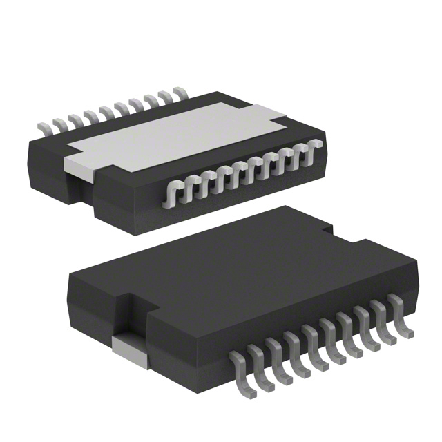
TLE 4471 is available in a Power PG-DSO-20 package. It is designed to supply
microprocessor systems under the severe condition of automotive applications and
therefore it is equipped with additional protection against overload, short circuit and
overtemperature. Of course the TLE 4471 can be used in other applications as well.
The TLE 4471 operates in the temperature range of Tj = -40 to 150 °C.
Type
Package
TLE 4471 G
Power PG-DSO-20
Data Sheet
1
Rev. 1.6, 2009-02-03
�TLE 4471
Self Protection - Over Temperature
- Short Circuit
- Reverse Polarity Proof
ESD Protection
I
E1
E2
E3
≥1
Main
Regulator
Tracker 1
Tracker 2
EN
5 V ±2%, 450 mA
Q1
100 mA, ±0.5% Tracking
Q2
Reference Voltage
REF2
50 mA, ±0.5% Tracking
Reference Voltage
Q3
REF3
Reset
Generator
Reset
Delay
DR
R
Reset
Level
Adjust
RADJ
W
Watchdog
DW
TLE 4471
AES02864
Figure 1
Data Sheet
Block Diagram
2
Rev. 1.6, 2009-02-03
�TLE 4471
GND
E1
I
Q2
REF2
R
DR
E2
Q1
GND
1
2
3
4
5
6
7
8
9
10
20
19
18
17
16
15
14
13
12
11
GND
DW
W
Q3
E3
REF3
EN
N.C.
RADJ
GND
AEP02865
Figure 2
Pin Configuration (top view)
Table 1
Pin Definitions and Functions
Pin No.
Symbol Function
1, 10, 11, GND
20
GROUND; all four pins connected to the heat sink
2
E1
Enable 1; Enable for Main Output Q1 and Q2; E1, E2 and E3 are
ored together; connect to GND, if not needed.
3
I
Input; block to ground directly at the IC for line compensation.
4
Q2
Tracking Output Q2; block to GND with min. 10 µF with
ESR < 3 Ω.
5
REF2
Reference Output; Reference Voltage related to Q2.
6
R
Reset Output; the open collector Output is connected to Q1 via an
integrated resistor.
7
DR
Reset Delay; connect a capacitor to GND for reset delay time
adjustment.
8
E2
Enable 2; Enable for Main Output Q1 and Q2; E1, E2 and E3 are
ored together; connect to GND, if not needed.
9
Q1
Main Output Q1; block to GND with min. 22 µF, ESR < 3 Ω.
12
RADJ
Reset Switching Threshold Adjust; The reset threshold can be
set individually with an external voltage divider at the pin. If it is
connected straight to GND the reset threshold remains at 4.65 V.
13
NC
Not Connected
Data Sheet
3
Rev. 1.6, 2009-02-03
�TLE 4471
Table 1
Pin Definitions and Functions (cont’d)
Pin No.
Symbol Function
14
EN
Enable Input; enables Q3
15
REF3
Reference Output; Reference Voltage related to Q3.
16
E3
Enable 3; Enable for Main Output Q1 and Q2; E1, E2 and E3 are
ored together; connect to GND, if not needed.
17
Q3
Tracker Output Q3; block to GND with min. 10 µF with ESR < 3 Ω.
18
W
Watchdog Trigger Input; positive edge triggered input for
monitoring a microcontroller.
19
DW
Watchdog Delay; connect a capacitor to GND for watchdog
trigger time adjustment.
Data Sheet
4
Rev. 1.6, 2009-02-03
�TLE 4471
Table 2
Absolute Maximum Ratings
Tj = -40 to 150 °C
Parameter
Symbol
Limit Values
Unit
Notes
–
Min.
Max.
-45
–
42
60
V
V
t < 400 ms
VQ1
IQ1
-0.3
7
V
–
–
–
mA
internally limited
VQ2
IQ2
-2
27
V
–
–
–
mA
internally limited
VQ3
IQ3
-2
27
V
–
-5
–
mA
internally limited
VE1
IE1
-0.3
16
V
–
-20
20
mA
–
VE2
IE2
-0.3
6.5
V
–
–
–
mA
internally limited
VE3
IE3
-0.3
16
V
–
-20
20
mA
–
VEN
IEN
-0.3
7
V
–
–
–
mA
internally limited
VREF2
IREF2
-0.3
4.5
V
–
–
–
mA
–
Input I
Input voltage
VI
Main Output Q1
Output voltage
Output current
Tracking Output Q2
Output voltage
Output current
Tracking Output Q3
Output voltage
Output current
Enable Input E1
Input voltage
Input current
Enable Input E2
Input voltage
Input current
Enable Input E3
Input voltage
Input current
Enable Input EN
Input voltage
Input current
Reference Output REF2
Output voltage
Output current
Data Sheet
5
Rev. 1.6, 2009-02-03
�TLE 4471
Table 2
Absolute Maximum Ratings (cont’d)
Tj = -40 to 150 °C
Parameter
Symbol
Limit Values
Unit
Notes
Min.
Max.
VREF3
IREF3
-0.3
4.5
V
–
–
–
mA
–
VRADJ
IRADJ
-0.3
7
V
–
–
–
mA
internally limited
VDR
-0.3
7
V
–
VR
-0.3
7
V
–
VDW
-0.3
7
V
–
VW
IW
-0.3
7
V
–
–
–
mA
–
Tj
TStg
-50
150
°C
–
-65
150
°C
–
Rthja
Rthjp
–
–
K/W
–
–
4
K/W
–
–
-2
2
kV
–
Reference Output REF3
Output voltage
Output current
Reset Adjust Input RADJ
Input Voltage
Input Current
Reset Delay DR
Voltage
Reset Output R
Voltage
Watchdog Delay DW
Voltage
Watchdog Input W
Input voltage
Input current
Temperature
Junction temperature
Storage temperature
Thermal Data
Junction-ambient
ESD
Human Body Model
Note: Stresses above those listed here may cause permanent damage to the device.
Exposure to absolute maximum rating conditions for extended periods may affect
device reliability.
Data Sheet
6
Rev. 1.6, 2009-02-03
�TLE 4471
Table 3
Operating Range
Parameter
Input voltage
Junction temperature
Shutdown voltage
threshold
Symbol
VI
Tj
Vshut
Limit Values
Unit
Notes
Min.
Max.
5.5
40
V
–
-40
150
°C
–
–
44
V
–
Note: In the operating range, the functions given in the circuit description are fulfilled.
Data Sheet
7
Rev. 1.6, 2009-02-03
�TLE 4471
Table 4
Characteristics
VI = 13.5 V; Tj = -40 °C < Tj < 125 °C
Parameter
Symbol
Limit Values
Min.
Typ. Max.
Unit Measuring Condition
Main Output Q1
Output voltage
VQ1
4.9
5.0
5.1
V
10 mA < IQ1 < 450 mA;
5.5 V < VI < 19 V
Output voltage
VQ1
4.8
5.0
5.2
V
10 mA < IQ1 < 300 mA;
5.5 V < VI < 28 V
Output voltage
VQ1
4.8
5.0
5.2
V
10 mA < IQ1 < 200 mA;
5.5 V < VI < 40 V
Output current limit
550
–
1500 mA
–
0.25
0.55
V
Line regulation
IQ1
VDR
∆VQ1
-25
–
25
mV
Load regulation
∆VQ1
-25
–
25
mV
Power Supply Ripple
Rejection
PSRR
–
30
–
dB
Output capacitor
CQ1
ESR
22
–
–
µF
2)
–
–
3
Ω
at 10 kHz2)
Output voltage
tracking accuracy
∆VQ2 =
VQ2 - VQ1
-25
–
25
mV
5.7 V < VI < 19 V;
1 mA < IQ2 < 100 mA
Output voltage
tracking accuracy
∆VQ2 =
VQ2 - VQ1
-25
–
25
mV
5.7 V < VI < 28 V;
1 mA < IQ2 < 80 mA
Output voltage
tracking accuracy
∆VQ2 =
VQ2 - VQ1
-25
–
25
mV
5.7 V < VI < 40 V;
1 mA < IQ2 < 50 mA
Output current limit
IQ2
VDR2
PSRR
110
–
–
mA
–
–
0.6
V
–
30
–
dB
VQ2 = 0.1 V
IQ2 = 100 mA
20 Hz < fr < 20 kHz;
VPP = 0.5 V;
CQ2 = 10 µF2)
Output voltage drop
ESR of output
capacitor
VQ1 = 0.1 V
IQ1 = 450 mA1)
8 V ≤ VI ≤ 16 V;
IQ1 = 10 mA
10 mA < IQ1 < 450 mA;
VI = 7 V
CQ1 = 22 µF;
20 Hz < fr < 20 kHz;
VPP = 0.5 V2)
Tracked Output Q2
Output voltage drop
Power Supply Ripple
Rejection
Data Sheet
8
Rev. 1.6, 2009-02-03
�TLE 4471
Table 4
Characteristics (cont’d)
VI = 13.5 V; Tj = -40 °C < Tj < 125 °C
Parameter
Symbol
Limit Values
Unit Measuring Condition
Min.
Typ. Max.
CQ2
ESR
10
–
–
µF
2)
–
–
3
Ω
at 10 kHz2)
Output voltage
tracking accuracy
∆VQ3 =
VQ3 - VQ1
-25
–
25
mV
5.7 V < VI < 19 V;
1 mA < IQ3 < 50 mA
Output voltage
tracking accuracy
∆VQ3 =
VQ3 - VQ1
-25
–
25
mV
5.7 V < VI < 28 V;
1 mA < IQ3 < 40 mA
Output voltage
tracking accuracy
∆VQ3 =
VQ3 - VQ1
-25
–
25
mV
5.7 V < VI < 40 V;
1 mA < IQ3 < 25 mA
Output current limit
IQ3
VDR3
PSRR
55
–
150
mA
–
–
0.6
V
–
30
–
dB
VQ3 = 0.1 V
1 mA ≤ IQ3 ≤ 50 mA
20 Hz < fr < 20 kHz;
VPP = 0.5 V;
CQ3 = 10 µF2)
CQ3
ESR
10
–
–
µF
2)
–
–
3
Ω
at 10 kHz2)
-25
–
25
mV
–
Iq
–
–
20
µA
Q1 OFF, Q2 OFF; Q3
OFF
Current consumption; Iq
Iq = II - IQ
–
1100 –
µA
Q3 OFF, IQ1 < 1 mA;
IQ2 < 1 mA
Current consumption; Iq
Iq = II - IQ
–
1800 –
µA
IQ1 < 10 mA;
IQ2 < 1 mA;
IQ3 < 1 mA
Output capacitor
ESR of output
capacitor
Tracked Output Q3
Output voltage drop
Power Supply Ripple
Rejection
Output capacitor
ESR of output
capacitor
Matching error
∆VQ2,3 =
between VQ2 and VQ3 VQ3 - VQ2
Current Consumption
Quiescent current
(standby)
Data Sheet
9
Rev. 1.6, 2009-02-03
�TLE 4471
Table 4
Characteristics (cont’d)
VI = 13.5 V; Tj = -40 °C < Tj < 125 °C
Parameter
Symbol
Limit Values
Unit Measuring Condition
Min.
Typ. Max.
3.5
4.1
4.5
V
VQ1 > 4.8 V; VQ2 > 4.8 V
1.5
–
2.5
V
–
–
50
–
µA
-1
–
5
µA
1.3
1.7
2.0
V
VE1 = 16 V
VE1 = 0 V
VQ1 > 4.8 V; VQ2 > 4.8 V
0.8
1.2
1.7
V
–
5
15
40
kΩ
–
3.5
–
4.5
V
VQ1 > 4.8 V; VQ2 > 4.8 V
1.5
–
2.5
V
–
–
50
–
µA
-1
–
5
µA
1.0
1.7
2.3
V
0.8
1.2
1.7
V
VE3 = 16 V
VE3 = 0 V
VQ3 > 4.8 V; Q1 ON
VQ3 < 0.1 V
5
15
40
kΩ
–
Enable Function E1, E2, E3, EN
VE1, on
VE1, off
E1 Off threshold
E1 High input current IE1, on
E1 Low input current IE1, off
VE2, on
E2 On threshold
E2 Off threshold
VE2, off
E2 resistance to GND RE2
VE3, on
E3 On threshold
E3 Off threshold
VE3, off
E3 High input current IE3, on
E3 Low input current IE3, off
EN On threshold
VEN, on
EN Off threshold
VEN, off
Enable resistance to REN
E1 On threshold
GND
Reset Generator
Switching threshold
VQ, rth
4.5
4.65
4.8
V
RADJ connected to
GND
Reset headroom
Vhead
RR
VR, low
250
350
500
mV
10 mA < IQ1 < 450 mA
2.4
–
6
kΩ
–
–
–
0.4
V
1 V < VQ1 < VQ, rth
Reset output Low
voltage
VR, low
–
–
0.4
V
VQ1 = 1 V, IR = 50 µA
Reset output High
voltage
VR, high
4.5
–
–
V
–
Reset adjust
threshold
VRADJ
1.25
1.35
1.45
V
VQ1 > 3.5 V
Reset pull-up
Reset output low
voltage
Data Sheet
10
Rev. 1.6, 2009-02-03
�TLE 4471
Table 4
Characteristics (cont’d)
VI = 13.5 V; Tj = -40 °C < Tj < 125 °C
Parameter
Symbol
Limit Values
Min.
Typ. Max.
Unit Measuring Condition
Reset delay charging
current
IDR, ch
2
4
6
µA
VDR = 1 V
Reset delay
discharge current
IDR, dis
60
120
160
mA
VDR = 1 V
Upper reset timing
threshold
VDR, dt
0.9
1.8
2.7
V
–
Lower timing
threshold
VDR, st
0.25
0.4
0.65
V
–
Reset delay time
tdr
trr
35
50
70
ms
0.5
–
3
µs
CR = 100 nF
CR = 100 nF
Watchdog input
pull-down resistor
RW
5
15
40
kΩ
–
Watchdog delay
charging current
IDW, ch
2
4
6
µA
VDW = 1 V; VDR = 2.7 V
Watchdog upper
timing threshold
VDW, dt
1.5
1.9
2.5
V
–
Watchdog lower
timing threshold
VDW, st
0
30
200
mV
–
Watchdog trigger
pulse interval
twp
35
50
70
ms
CDW = 100 nF
49.5
50
50.5
% of –
Reset reaction time
Watchdog
Reference Output REF2
Voltage divider ratio
VREF2
VQ2
Output impedance
RREF2
Output clamp voltage –
Data Sheet
10
–
20
kΩ
–
–
–
4.5
V
–
11
Rev. 1.6, 2009-02-03
�TLE 4471
Table 4
Characteristics (cont’d)
VI = 13.5 V; Tj = -40 °C < Tj < 125 °C
Parameter
Symbol
Limit Values
Min.
Typ. Max.
49.5
50
Unit Measuring Condition
Reference Output REF3
Voltage divider ratio
VREF3
50.5
% of –
VQ3
Output impedance
RREF3
Output clamp voltage –
10
–
20
kΩ
–
–
–
4.5
V
–
1) Measured when the output voltage VQ dropped 100 mV from the nominal value.
2) Not subject to production test, specified by design.
Note: The listed characteristics are ensured over the operating range of the integrated
circuit. Typical characteristics specify mean values expected over the production
spread. If not otherwise specified, typical characteristics apply at TA = 25 °C and
the given supply voltage.
Data Sheet
12
Rev. 1.6, 2009-02-03
�TLE 4471
II
IQ1
VI
I
VQ1
Q1
22 µF
IE1
VE1
E1
IQ2
IE2
VQ2
Q2
VE2
E2
IE3
10 µF
IREF2
TLE 4471
VE3
E3
VEN
VREF2
REF2
IEN
EN
IQ3
IDR, dis
IRADJ
CDR
100 nF
10 µF
IDR, ch
VRADJ
VQ3
Q3
DR
IREF3
RADJ
VREF3
REF3
IW
VW
W
IR
CDW
100 nF
DW
IDW, ch
GND
R
VR
IGND
AES02866
Figure 3
Data Sheet
Measurement Circuit
13
Rev. 1.6, 2009-02-03
�TLE 4471
Application Information
Q2
VBAT KL. 30
I
Tracking
Output 2
Sensor /
Peripheral
REF2
optional
Main
Q1
RADJ
DR
Watchdog /
Reset
DW
Ignition KL. 15
Enable-Signal
AD
E1
Enable
Logic
E3
R
W
Controller
E2
EN
AD
REF3
Tracking
Output 3
Q3
Sensor /
Peripheral
AES02867
Figure 4
Application Diagram
Input
With an input voltage between 5.5 V < VI < 40 V the regulator works in its normal
operating range. If the input voltage exceeds the 40 V up to 60 V for less than 400 ms,
e.g. caused by a load dump, the active components are switched off.
For compensating line influences and to avoid steep input edges above 1 V/µs an input
capacitor is needed. Using a resistor of approx. 1 Ω in series to the input capacitor, the
oscillating circuit consisting of input inductance and input capacitor is damped.
Data Sheet
14
Rev. 1.6, 2009-02-03
�TLE 4471
Output Voltage
To obtain an output voltage of VQ1 = 5 V with an accuracy of 2% at the main output Q1
an input voltage in the range of 5.5 V < VI < 40 V is needed. The main output Q1 supplies
5 V with 450 mA current capability. For stability it requires an output capacitor of at least
22 µF and a maximum ESR of 3 Ω. The two outputs Q2 and Q3 are tracked to Q1 and
can supply currents of 100 mA and 50 mA. So any undervoltage condition or shutdown
of Q1 will cause the same effect to Q2 and Q3. For Stability both outputs require an
output capacitor of at least 10 µF with ESR < 3 Ω each. Q2 is switched on and off
simultaneously with Q1, while the tracked output Q3 can be enabled or disabled
individually.
Two reference outputs REF2, REF3 with voltages of VREF2 = VQ2/2 and VREF3 = VQ3/2 are
also available. In case of an overvoltage at the tracker outputs, the voltage references
are limited internally to 4.5 V.
Output Current
The output current is a function of the input voltage. For high input voltages above 22 V,
the output current is reduced linear. This is designed into the regulator for protection.
Above 42 V the regulator is switched off. The thermal shutdown switches the regulator
off, if it exceeds the thermal threshold of 160 °C typical. It is switched on again, as soon
as the regulator is cooled down by typical 10 K (thermal hysteresis). Please note the
device should not be operated above a junction temperature of 150 °C for long term
reliability.
Enable Function
The TLE 4471 includes the possibility of enabling the main and tracked outputs.
Three ORed enable inputs E1, E2, E3 are used to control the main output Q1 and the
tracked output Q2. E1 and E3 can be supplied from the battery line or ignition key with
input voltages up to 16 V. The enable inputs should be protected by a series resistor and
a capacitor, e.g. RE1 = RE3 = 22 kΩ, CE1 = CE3 = 2.2 nF. E2 is intended for connection to
the microcontroller. A logic HIGH at any enable input will switch on the related regulator
and/or tracker.
A separate enabling pin EN is available to switch on and off the second tracked output
Q3 separately by the microcontroller.
Reset
The power on reset feature is necessary for a defined start of the microprocessor during
power up. When the output voltage of the main regulator has reached the reset threshold
voltage the reset delay capacitor CDR is charged. After a certain time, the reset delay time
tdr, the voltage at the capacitor equals the upper reset timing threshold and the reset
output goes HIGH.
Data Sheet
15
Rev. 1.6, 2009-02-03
�TLE 4471
The reset delay time tdr is defined by the reset delay capacitor CDR at pin DR and can be
calculated as follows:
VDR ,dt
t rd = C DR × -------------I DR ,ch
(1)
Definitions:
CDR = reset delay capacitor
tdr = reset delay time required by the application
VDR, dt = typical 1.8 V for power up reset
IDR, ch = charge current typical 4 µA
For a delay capacitor CDR = 100 nF the typical power up reset delay time is 45 ms.
The undervoltage reset circuitry supervises the output voltage. In case VQ1 falls below
the reset threshold the reset output is set LOW after the reset reaction time trr (discharge
of the reset delay capacitor). The reset LOW signal is held down to an output voltage VQ1
•
•
•
•
of 1 V. Both, the reset reaction time and the reset delay time are defined by the capacitor
value.
The reset reaction time trr is the time it takes the voltage regulator to set its reset output
LOW after the output voltage has dropped below the reset threshold. The reset reaction
time can be calculated using the following equation:
V DR ,dt – V DR ,st
t rr = C DR × ----------------------------------I DR ,dis
Data Sheet
(2)
16
Rev. 1.6, 2009-02-03
�TLE 4471
VΙ
t
< t rr
VQ
V Q, rth
t
VD
VDR, dt
VDR, st
V RO
t dr
t rr
t
t
Power-on-Reset
Figure 5
Thermal
Shutdown
Voltage Dip
at Input
Undervoltage
Secondary
Spike
Overload
at Output
AED03045
Reset Timing
The reset output is an open collector output with a pull-up-resistor of typical 4 kΩ to Q1.
An external pull-up can be added with a resistor value of at least 20 kΩ.
In addition the reset switching threshold can be adjusted by an external voltage divider.
The feature is useful with microprocessors which guarantee safe operation down to
voltages below the internally set reset threshold of 4.65 typical.
Data Sheet
17
Rev. 1.6, 2009-02-03
�TLE 4471
TLE 4471
I
Q
Bandgap
Reference
RRTH1
1.36 V
R
Vrth,ref
1
RADJ
RRTH2
AES02877
Figure 6
Adjusting the Reset Threshold
For using the preadjusted reset threshold voltage of typical VQ, rth = 4.65 V, the pin RADJ
has to be connected to GND.
If a lower reset threshold is required by the system, a voltage divider defines the reset
threshold VQ, rthext between 3.5 V and 4.65 V:
RRTH1
V Q, rthext = V rth ,ref × 1 + -------------RRTH2
(3)
Vrth,ref is typical 1.35 V.
Data Sheet
18
Rev. 1.6, 2009-02-03
�TLE 4471
Watchdog
The reset and watchdog timing can be defined independently of each other by two delay
capacitors CDR and CDW at pins DR and DW.
The watchdog function supervises the microcontroller including time base failures. If
there is no positive edge within a certain pulse repetition time twp or the trigger pulse is
too short a reset is generated. Programming of the max. repetition time is done by a
delay capacitor CDW at pin DW.
The frequency of the watchdog pulses generated by the microcontroller has to be higher
than the minimum pulse sequence twp set by the external reset delay capacitor CDW. The
pulse repetition time can be calculated as follows:
V DW ,dt – V DW ,st
t wp = C DW × ------------------------------------I DW ,ch
(4)
VI
t
VQ1
t
t > 10 µs
t > 25 µs
VW
t
tWP
VDW
VDW,dt
t
VDR
tdr
trr
t
VDW,st
VDR,dt
VDR,st
VR
Missing edge
at Watchdog
Watchdog pulses
too short
t
AET03000
Figure 7
Watchdog Timing
If the watchdog is not used in an application the pin WD has to be connected to GND.
Data Sheet
19
Rev. 1.6, 2009-02-03
�TLE 4471
Power Supply Ripple Rejection PSRR of
Main Output Q1 versus Frequency f
Power Supply Ripple Rejection PSRR of
Output Q2 versus Frequency f
AED02995
80
dB CQ1 = 22 µF
PSRR
AED02996
80
dB CQ2 = 10 µF
PSRR
I Q1 = 10 mA
70
70
I Q1 = 450 mA
IQ2 = 1 mA
60
60
50
50
IQ2 = 100 mA
40
40
30 0
10
10
1
10
2
10
3
4
10 Hz 10
f
30 0
10
5
101
102
103
Hz 105
f
Power Supply Ripple Rejection PSRR of
Output Q3 versus Frequency f
AED02997
80
dB CQ3 = 10 µF
PSRR
70
IQ3 = 1 mA
60
50
40
IQ3 = 50 mA
30 0
10
Data Sheet
101
102
103
Hz 105
f
20
Rev. 1.6, 2009-02-03
�TLE 4471
Enable Currents IE1, IE3 and Output
Voltage VQ1 versus Enable Voltages
VE1, VE3
IE1, IE3
AED02998
5
µA
7.5
V
Enable Currents IE2, IEN and Output
Voltage VQ3 versus Enable Voltages
VE2, VEN
AED02999
250
µA
VQ1
IE2, IEN
7.5
V
4
6
200
6
3
4.5
150
4.5
2
3
100
3
1
1.5
0
0
1
2
3
4 V
0
0
VE1, VE3
Data Sheet
1.5
50
0
5
21
VQ3
0.5
1
1.5
0
2 V 2.5
VE2, VEN
Rev. 1.6, 2009-02-03
�TLE 4471
Package Outlines
+0.07
-0.02
3.5 MAX.
6.3
0.1
5˚ ±3˚
0.25
1.3
15.74 ±0.1
(Heatslug)
B
2.8
Heatslug
(Mold)
0.95 ±0.15
0.25 M A 20x
20
11
1
10
14.2 ±0.3
Bottom View
11
0.25 B
20
5.9 ±0.1
(Metal)
0.4 +0.13
3.2 ±0.1
(Metal)
1.27
3.25 ±0.1
0 +0.1
1.1 ±0.1
11 ±0.15 1)
Index Marking
1 x 45˚
15.9 ±0.15 1)
(Mold)
1)
10
A
13.7 -0.2
(Metal)
1
Heatslug
Does not include plastic or metal protrusion of 0.15 max. per side
GPS05791
Figure 8
Power PG-DSO-20 (Plastic Dual Small Outline)
Green Product (RoHS compliant)
To meet the world-wide customer requirements for environmentally friendly products
and to be compliant with government regulations the device is available as a green
product. Green products are RoHS-Compliant (i.e Pb-free finish on leads and suitable
for Pb-free soldering according to IPC/JEDEC J-STD-020).
Find all of our packages, sorts of packing and others in our Infineon
Internet Page “Packages”: http://www.infineon.com/packages.
Dimensions in mm
SMD = Surface Mounted Device
Data Sheet
22
Rev. 1.6, 2009-02-03
�TLE 4471
Revision History
Version
Date
Rev. 1.6
2009-02-03 Package bond wire modification according
to PCN No. 2007-090. Change of package name in
datasheet to “Power PG-DSO-20”. No change of package
outline.
Rev. 1.5
2007-03-20 Initial version of RoHS-compliant derivate of TLE 4471
Page 1: AEC certified statement added
Page 1 and Page 22: RoHS compliance statement and
Green product feature added
Page 1 and Page 22: Package changed to RoHS compliant
version
Legal Disclaimer updated
Rev. 1.4
2005-01-28 Parameter “Output Clamp Voltage” REF2 and REF3:
Max. value changed from 4V to 4.5V in order to align with the
Maximum Ratings
Data Sheet
Changes
23
Rev. 1.6, 2009-02-03
�Edition 2009-02-03
Published by
Infineon Technologies AG
81726 Munich, Germany
© 2009 Infineon Technologies AG
All Rights Reserved.
Legal Disclaimer
The information given in this document shall in no event be regarded as a guarantee of conditions or
characteristics. With respect to any examples or hints given herein, any typical values stated herein and/or any
information regarding the application of the device, Infineon Technologies hereby disclaims any and all warranties
and liabilities of any kind, including without limitation, warranties of non-infringement of intellectual property rights
of any third party.
Information
For further information on technology, delivery terms and conditions and prices, please contact the nearest
Infineon Technologies Office (www.infineon.com).
Warnings
Due to technical requirements, components may contain dangerous substances. For information on the types in
question, please contact the nearest Infineon Technologies Office.
Infineon Technologies components may be used in life-support devices or systems only with the express written
approval of Infineon Technologies, if a failure of such components can reasonably be expected to cause the failure
of that life-support device or system or to affect the safety or effectiveness of that device or system. Life support
devices or systems are intended to be implanted in the human body or to support and/or maintain and sustain
and/or protect human life. If they fail, it is reasonable to assume that the health of the user or other persons may
be endangered.
�