Dual Low Drop Voltage Regulator
TLE 4473 GV53
TLE 4473 GV52
Features
•
•
•
•
•
•
•
•
•
•
•
•
Output 1: 300 mA, 3.3 V (±3%) or 2.6 V (±3%)
Output 2: 180 mA, 5 V (±2%)
Low quiescent current consumption
Disable function separately for both outputs
Wide operation range: up to 42 V
Very low dropout voltage
2 independent reset circuits
Watchdog
Output protected against short circuit
Wide temperature range: -40 °C to 150 °C
Overtemperature protection
Overload protection
Functional Description
The TLE 4473 is a monolithic integrated voltage regulator with two very low-drop
outputs, Q1 for loads up to 300 mA and Q2 providing a maximum of 180 mA. An input
voltage in the range of 5.6 V ≤ VI ≤ 45 V is transformed to VQ2 = 5.0 V (±2%) and
VQ1 = 3.3 V ±3% (TLE 4473 GV53) or VQ1 = 2.6 V ±3% (TLE 4473 GV52). The device is
also available with dual 5 V output voltage, please refer to the TLE 4473 GV55 data
sheet. Two inhibit pins allow a flexible power management. Both outputs can
independently be enabled or disabled. Thus the current consumption of the application
can be reduced to a minimum. The quiescent current of the TLE 4473 with both outputs
disabled is < 1 µA. The TLE 4473 is designed to supply microprocessor systems and
sensors under the severe conditions of automotive applications and is therefore
equipped with additional protection functions against overload, short circuit and
overtemperature.
The device operates in the wide junction temperature range of -40 °C to 150 °C.
Type
Package
TLE 4473 GV53
PG-DSO-12
TLE 4473 GV52
PG-DSO-12
Data Sheet
1
Rev. 1.1, 2008-09-19
�TLE 4473 GV53
TLE 4473 GV52
The low drop regulator features a reset with adjustable power on delay for each of the
outputs. In addition the output for the microcontroller supply comes up with a watchdog
in order to supervise a microcontroller.
VBat
TLE 4473 GV53 / TLE 4473 GV52
7 I
Q2 4
10
µF
Overtemperature
Shutdown
Bandgap
Reference
Current and
Saturation
Control,
Overcurrent
Protection
e. g. µC I/O
or Sensor
Supply
4.7 kΩ
Reset
Generator
RO2 2
?1
D2 10
µC
9 INH2
Inhibit
100 nF
Q1 5
22 µF
or
10 µF
Current and
Saturation
Control,
Overcurrent
Protection
Ignition
8 INH1
Reset
Generator
Watchdog
Inhibit
µC Core
Supply
4.7 kΩ
RO1 3
µC
Reset
WI 1
Watchdog
(from µC)
D1 11
100 nF
6, 12
GND
Figure 1
Data Sheet
AEB03507.VSD
Block Diagram with Typical External Components
2
Rev. 1.1, 2008-09-19
�TLE 4473 GV53
TLE 4473 GV52
Reset and Watchdog Behaviour:
The reset output RO1 is in high-state if the voltage on the delay capacitor CD1 is greater
or equal VDL1. The delay capacitor CD1 is charged with the current IDC1 for output voltages
greater than the reset threshold VRT1. If the output voltage drops below VRT1 (“reset
condition”), the delay capacitor CD1 will be discharged rapidly. If VD1 reaches VDL1, the
reset output RO1 is set to low.
At power-on, the charging process of CD1 starts from 0 V, which leads to the equation
C D1 × V DU1
t D, on = ---------------------------I DC1
(1)
for the power-on reset delay time.
When the voltage at the delay capacitor has reached VDU1 and RO1 was set to high, the
watchdog circuit is enabled and discharges CD1 with the constant current IDD1.
If there is no rising edge observed at the watchdog input, CD1 will be discharged down to
VDL1, where the reset output RO1 will be set to low and CD1 will be charged again with
the current IDC1 until VD1 reaches VDU1 and reset will be set high again.
If a watchdog pulse (rising edge at watchdog input WI) occurs during the discharge
period, CD1 is charged again and the reset output stays high. After VD1 has reached VDU1,
the periodical cycle starts again.
The watchdog timing is shown in Figure 2. The maximum duration between two
watchdog pulses corresponds to the minimum watchdog trigger time TWI,tr. Higher
capacitances on pin D1 result in larger watchdog trigger time:
T WI,tr
max
= 0.42 ms/nF × C D1
(2)
If the output voltage Q2 decreases below VRT2 , the external capacitor CD2 is discharged.
When the voltage at this capacitor drops below VDL2, a reset signal is generated at pin
11 (RO2), i.e. the reset output is set to low-level. If the output voltage rises above the
reset threshold, CD2 will be charged with the constant current IDC2. After the power-onreset time, the voltage at the capacitor reaches VDU2 and the reset output will be set to
high again. The value of the power-on-reset time can be set within a wide range
depending of the capacitance of CD2 using Equation (1) analogous for Q2.
Data Sheet
3
Rev. 1.1, 2008-09-19
�TLE 4473 GV53
TLE 4473 GV52
VW Ι
t
VΙ
VQ
t
T WD, p
VD1
t
T WI, tr
VDU1
VDL1
t WD, L
VWO
T WI, tr =
(VDU1 - VDL1)
Ι DD1
C D1 ; T WD, p =
(VDU1 - VDL1) (Ι DC1 + Ι DD1 )
Ι DC1 x Ι DD1
C D1 ; t WD, L =
t
(VDU1 - VDL1)
Ι DC1
t
C D1
AED03099_4473gv53
Figure 2
Data Sheet
Watchdog Timing Schedule
4
Rev. 1.1, 2008-09-19
�TLE 4473 GV53
TLE 4473 GV52
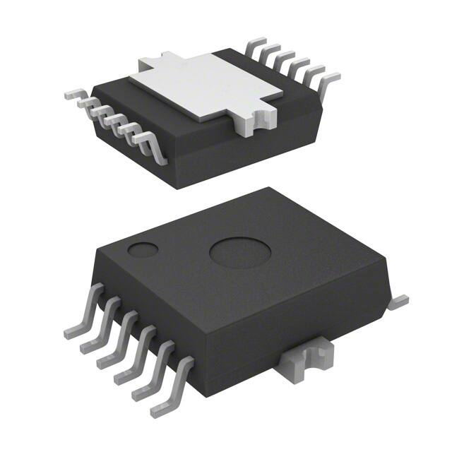
P-DSO-12-6
WI
1
12
GND
RO2
2
11
D1
RO1
3
10
D2
Q2
4
9
INH2
Q1
5
8
INH1
N.C.
6
7
I
AEP03318_4473gv53.VSD
Pin 6 and heat slug should be connected to GND
Figure 3
Pin Configuration TLE 4473 GV53, TLE 4473 GV52 (top view)
Table 1
Pin Definitions and Functions (TLE 4473 GV53, TLE 4473 GV52)
Pin No.
Symbol Function
1
WI
Watchdog input; input for watchdog pulses, positive edge
triggered
2
RO2
Reset output for Q2; open collector output
3
RO1
Reset and watchdog output for Q1; open collector output
4
Q2
Output voltage 2 (5 V); block to GND with a capacitor CQ2 ≥ 22 µF,
ESR < 5 Ω at 10 kHz or CQ2 ≥ 10 µF, ESR < 4 Ω at 10 kHz
5
Q1
Output voltage 1 (3.3 V/2.6 V); block to GND with a capacitor
CQ1 ≥ 10 µF, ESR < 5 Ω at 10 kHz
6
N.C.
Not connected; connect to GND
7
I
Input voltage; block to GND directly at the IC with a ceramic
capacitor.
8
INH1
Inhibit input 1; low level at INH2 and INH1 disables Q2 and Q1
9
INH2
Inhibit input 2; low level disables Q2
10
D2
Reset Delay 2; connect a capacitor to set reset delay for Q2
11
D1
Reset Delay 1; connect a capacitor to GND to set reset delay and
watchdog timing for Q1
12
GND
Ground
Heatsink
N. C.
Not connected; connect to GND
Data Sheet
5
Rev. 1.1, 2008-09-19
�TLE 4473 GV53
TLE 4473 GV52
Table 2
Absolute Maximum Ratings
-40 °C < Tj < 150 °C
Parameter
Symbol
Limit Values
Unit
Remarks
Min.
Max.
VI
II
-42
45
V
–
–
–
mA
Internally limited
VQ2
IQ2
-0.3
18
V
–
–
–
mA
Internally limited
VQ1
IQ1
-0.3
18
V
–
–
–
mA
Internally limited
VINH1
IINH1
-42
45
V
–
-2
2
mA
–
VINH2
IINH2
-42
45
V
–
-2
2
mA
–
VRO1
IRO1
-0.3
18
V
–
–
–
mA
Internally limited
VRO2
IRO2
-0.3
18
V
–
–
–
mA
Internally limited
VD1
ID1
-0.3
7
V
–
-5
5
mA
–
VD
ID
-0.3
7
V
–
-5
5
mA
–
Input I
Voltage
Current
Stand-by Output Q2
Voltage
Current
Main Output Q1
Voltage
Current
Inhibit Input INH1
Voltage
Current
Inhibit Input INH2
Voltage
Current
Reset Output RO1
Voltage
Current
Reset Output RO2
Voltage
Current
Reset Delay D1
Voltage
Current
Reset Delay D2
Voltage
Current
Data Sheet
6
Rev. 1.1, 2008-09-19
�TLE 4473 GV53
TLE 4473 GV52
Table 2
Absolute Maximum Ratings (cont’d)
-40 °C < Tj < 150 °C
Parameter
Symbol
Limit Values
Unit
Remarks
Min.
Max.
VRADJ
IRADJ
-0.3
7
V
–
-5
5
mA
–
Tj
Tstg
-40
150
°C
–
-50
150
°C
–
VESD
–2
2
kV
Human Body Model
Watchdog Input WI
Voltage
Current
Temperatures
Junction temperature
Storage temperature
ESD Protection
Electrostatic Discharge
Voltage
Note: Maximum ratings are absolute ratings; exceeding any one of these values may
cause irreversible damage to the integrated circuit.
Data Sheet
7
Rev. 1.1, 2008-09-19
�TLE 4473 GV53
TLE 4473 GV52
Table 3
Operating Range
Parameter
Symbol
Limit Values
Unit
Remarks
Min.
Max.
5.6
42
V
Q1 & Q2
4.5
42
V
only Q1 regulating
-40
150
°C
–
–
3
K/W
–
Junction ambient
Rthj-pin
Rthj-a
–
115
K/W
PCB Heat Sink
Area 0 mm2 1)
Junction ambient
Rthj-a
–
100
K/W
PCB Heat Sink
Area 100 mm2 1)
Junction ambient
Rthj-a
–
60
K/W
PCB Heat Sink
Area 300 mm2 1)
Junction ambient
Rthj-a
–
48
K/W
PCB Heat Sink
Area 600 mm2 1)
Input voltage
Junction temperature
VI
Tj
Thermal Resistances PG-DSO-12
Junction pin
1) Package mounted on PCB 80 × 80 × 1.5 mm3; 35 µ Cu; 5 µ Sn; zero airflow.
Note: In the operating range the functions given in the circuit description are fulfilled.
Integrated protection functions are designed to prevent IC destruction under fault
conditions. Protection functions are not designed for repetitive operation.
Data Sheet
8
Rev. 1.1, 2008-09-19
�TLE 4473 GV53
TLE 4473 GV52
Electrical Characteristics
VI1 =13.5 V; VINH1 =VINH2= 5V; – 40 °C < Tj < 150 °C; unless otherwise specified
Parameter
Symbol
Limit Values
min.
typ.
max.
Unit Test Condition
REGULATOR 2:
Output Q2
Output voltage
VQ2
4.90
5.0
5.10
V
1 mA < IQ2< 180 mA;
6 V < VI < 28 V
Output current
limitation
IQ2
200
300
600
mA
VQ2 = 4.5 V
–
300
600
mV
IQ2 = 100 mA; 1)
Output drop voltage; VDRQ2
VDRQ2 = VI2 – VQ2
Load regulation
∆VQ2,Lo
–
15
50
mV
1 mA < IQ2 < 200 mA;
Line regulation
∆VQ2,Li
–
5
20
mV
IQ2 = 1 mA;
6 V < VI < 28 V
Power supply ripple
rejection
PSRR
–
65
–
dB
fr = 100 Hz;
Vr = 1 Vpp
–
165
µA
TLE 4473 GV52;
IQ2 = 500 µA; Tj = 25 °C;
VINH1 < VINH1 OFF (Q1 off)
–
205
µA
TLE 4473 GV52;
IQ2= 500 µA; Tj = 85 °C;
Current Consumption
Quiescent current;
stand-by
Iq = II – IQ2
Iq
VINH1 < VINH1 OFF (Q1 off)
–
180
µA
TLE 4473 GV53;
IQ2 = 500 µA; Tj = 25 °C;
VINH1 < VINH1 OFF (Q1 off)
–
210
µA
–
235
µA
TLE 4473 GV53;
IQ2= 500 µA; Tj = 85 °C;
VINH1 < VINH1 OFF (Q1 off)
IQ2 = 500 µA;
VINH1 < VINH1 OFF (Q1 off)
Data Sheet
9
Rev. 1.1, 2008-09-19
�TLE 4473 GV53
TLE 4473 GV52
Electrical Characteristics (cont’d)
VI1 =13.5 V; VINH1 =VINH2= 5V; – 40 °C < Tj < 150 °C; unless otherwise specified
Parameter
Symbol
Limit Values
min.
typ.
Unit Test Condition
max.
Current Consumption (cont’d)
Quiescent current;
stand-by
Iq = II – IQ2
Iq
Quiescent current;
inhibited
Iq
–
–
1
µA
VINH1=VINH2= 0V;
TJ < 85°C
VINH2 ON
VINH2 OFF
IINH2 ON
IINH2 OFF
–
–
2.3
V
VQ2 on
0.8
–
–
V
VQ2 off
–1
0.5
3
µA
–1
0.1
1
µA
VINH2 = 5 V
0 V < VINH2 < 0.8 V
IDC2
VDU2
5.0
9.0
13.0
µA
VD2 = 0.7 V
1.6
1.8
2.2
V
–
Lower timing
threshold
VDL2
0.3
0.45
0.6
V
–
Saturation Voltage
VD2,SAT
100
mV
VQ2 < VRT2
Reset delay time
TRD2
12
28
ms
Reset reaction time
Trr
–
10
µs
CD2 = 100 nF
CD2 = 100 nF
5
mA
IQ2 = 100 mA;
VINH1 < VINH1 OFF(Q1 off)
Inhibit Input INH2
Turn-on Voltage
Turn-off Voltage
H-input current
L-input current
Reset Timing D2
Charge current
Upper timing
threshold
Data Sheet
20
10
Rev. 1.1, 2008-09-19
�TLE 4473 GV53
TLE 4473 GV52
Electrical Characteristics (cont’d)
VI1 =13.5 V; VINH1 =VINH2= 5V; – 40 °C < Tj < 150 °C; unless otherwise specified
Parameter
Symbol
Limit Values
Unit Test Condition
min.
typ.
max.
4.5
4.65
4.8
V
–
–
–
1.4
mA
Collector current of RO1,
power good, reset still
delayed.
VQ2=5V, VD2=0V,VRO2=0.3V
–
0.15
0.3
V
VQ2 ≥ 1 V, VD2=0V,
Reset Output RO2
Reset switching
threshold
VRT2
Reset output current IRO2
Reset output low
voltage
VRO2L
Reset high voltage
VRO2H
4.5
–
–
V
RRO2,ext=4.7kΩ
Output voltage
VQ12
3.20
3.3
3.40
V
TLE 4473 GV53
1 mA < IQ1< 300 mA;
4.5 V < VI < 28 V
Output voltage
VQ12
2.52
2.60
2.68
V
TLE 4473 GV52
1 mA < IQ1< 300 mA;
4.5 V < VI < 28 V
Output current
limitation
IQ1
350
500
600
mA
VQ1 = 3.0 V
(TLE 4473 GV53);
VQ1 = 2.3 V
(TLE 4473 GV52)
Load regulation
∆VQ1,Lo
–
5
50
mV
5 mA < IQ1 < 300 mA;
Line regulation
∆VQ1,Li
–
5
20
mV
IQ1 = 5 mA;
6 V < VI< 28 V
Power-SupplyRipple-Rejection
PSRR
–
65
–
dB
fr = 100 Hz;
Vr = 1Vpp
IRO2= 0.5mA
REGULATOR 1:
Output Q1
Data Sheet
11
Rev. 1.1, 2008-09-19
�TLE 4473 GV53
TLE 4473 GV52
Electrical Characteristics (cont’d)
VI1 =13.5 V; VINH1 =VINH2= 5V; – 40 °C < Tj < 150 °C; unless otherwise specified
Parameter
Symbol
Limit Values
min.
typ.
max.
–
200
265
Unit Test Condition
Current Consumption
Quiescent current;
Iq = II – IQ1– IQ2
Iq
µA
TLE 4473 GV52;
IQ1 = 500 µA;
Q1 on; Q2 off; Tj < 85°C
–
210
280
µA
TLE 4473 GV53;
IQ1 = 500 µA;
Q1 on; Q2 off; Tj < 85°C
–
7
20
mA
IQ1 = 300 mA
IQ2 = 500 µA,
VQ1 & VQ2 on
–
250
500
µA
IQ2 = IQ1 = 500 µA;
VQ1 & VQ2 on
Inhibit Input INH1
Turn-on Voltage
Turn-off Voltage
H-input current
L-input current
VINH1 ON
VINH1 OFF
IINH1 ON
IINH1 OFF
–
–
2.3
V
VQ1 on
0.8
–
–
V
VQ1 off
–1
0.5
3
µA
–1
0.1
1
µA
VINH1= 5 V
0 V < VINH1< 0.8 V
Watchdog and Reset Timing D1
Charge current
Discharge current
Upper timing
threshold
Lower timing
threshold
Data Sheet
IDC1
IDD1
VDU1
3.0
7.0
11.0
µA
1.1
1.5
3.7
µA
VD1 = 0.7 V
VD1 = 0.7 V
0.7
1.1
1.6
V
–
VDL1
0.2
0.35
0.6
V
–
12
Rev. 1.1, 2008-09-19
�TLE 4473 GV53
TLE 4473 GV52
Electrical Characteristics (cont’d)
VI1 =13.5 V; VINH1 =VINH2= 5V; – 40 °C < Tj < 150 °C; unless otherwise specified
Parameter
Symbol
Limit Values
min.
typ.
Unit Test Condition
max.
Watchdog and Reset Timing D1 (cont’d)
Saturation Voltage
VD1,SAT
Watchdog trigger
time
TWI,tr
24
Reset delay time
TRD1
11
Reset reaction time
Trr
–
VRT1
2.97
100
mV
VQ1 < VRT2
32
40
ms
CD1 = 100 nF
17
23
ms
5.0
µs
CD1 = 100 nF
CD1 = 100 nF
3.08
3.18
V
TLE 4473 GV53
2.34
2.42
2.50
V
TLE 4473 GV52
Reset Output RO1
Reset switching
threshold
Reset threshold
headroom
VR1HEAD
100
–
–
mV
TLE 4473 GV53
Reset threshold
headroom
VR1HEAD
80
–
–
mV
TLE 4473 GV52
–
–
1.4
mA
Collector current of RO1,
power good, reset still
delayed.
VQ1= 3.30 V
(TLE 4473 GV53),
VQ1 = 2.60 V
(TLE 4473 GV52);
VQ2=5.0 V;
VD1=0 V,VRO1=0.3 V
–
0.1
0.3
V
VQ1 ≥ 1 V, VD1=0V,
Reset output current IRO1
Reset output low
voltage
VRO1L
Reset output high
voltage
VRO1H
2.45
–
–
V
RRO1,ext=4.7kΩ connected
to Q1;TLE 4473 GV52
Reset output high
voltage
VRO1H
3.15
–
–
V
RRO1,ext=4.7kΩ connected
to Q1;TLE 4473 GV53
IRO1=0.5mA
1) Drop voltage = VI – VQ (measured when the output voltage has dropped 100 mV from the nominal value
obtained at 13.5 V input)
Data Sheet
13
Rev. 1.1, 2008-09-19
�TLE 4473 GV53
TLE 4473 GV52
C
0.1
12x
7.8 ±0.1
0.1 C
(Heatslug)
Seating Plane
5˚ ±3˚
35
B
+0.075
0.25 -0
.0
7.5 ±0.11)
0.1±0.05
STANDOUT
(1.55)
0.8
0 +0.1
STANDOFF
2.35 ±0.1
2.6 MAX.
Package Outlines
(0.2)
0.7 ±0.15
10.3 ±0.3
0.25 B
12
Index Marking
12x
0.25
M
C A B
0.4
A
7
7
1
6
6
12
4.2 ±0.1
6.4 ±0.11)
1.6 ±0.1
Bottom View
1
Heatslug
1
+0.13
5.1±0.1
5x 1=5
1) Does not include plastic or metal protrusion of 0.15 max. per side
PG-DSO-12-4, -5, -8, -11, -12, -16-PO V04
Figure 4
PG-DSO-12 (Plastic Dual Small Outline)
Green Product (RoHS compliant)
To meet the world-wide customer requirements for environmentally friendly products
and to be compliant with government regulations the device is available as a green
product. Green products are RoHS-compliant (i.e Pb-free finish on leads and suitable for
Pb-free soldering according to IPC/JEDEC J-STD-020).
Data Sheet
14
Rev. 1.1, 2008-09-19
�TLE 4473 GV53
TLE 4473 GV52
Revision History
Version
Date
Changes
Rev. 1.1
2008-19-09 Initial version of RoHS-compliant derivate of TLE 4473 GV53
Page 1: AEC certified statement added
Page 1 and Page 14: RoHS compliance statement and
Green product feature added
Page 1 and Page 14: Package changed to RoHS compliant
version
Legal Disclaimer updated
Rev. 1.0
2004-07-14 Initial version
You can find all of our packages, sorts of packing and others in our
Infineon Internet Page “Products”: http://www.infineon.com/products.
Dimensions in mm
SMD = Surface Mounted Device
Data Sheet
15
Rev. 1.1, 2008-09-19
�Edition 2008-09-19
Published by
Infineon Technologies AG
81726 München, Germany
© Infineon Technologies AG 2008.
All Rights Reserved.
Legal Disclaimer
The information given in this document shall in no event be regarded as a guarantee of conditions or
characteristics (“Beschaffenheitsgarantie”). With respect to any examples or hints given herein, any typical values
stated herein and/or any information regarding the application of the device, Infineon Technologies hereby
disclaims any and all warranties and liabilities of any kind, including without limitation warranties of
non-infringement of intellectual property rights of any third party.
Information
For further information on technology, delivery terms and conditions and prices please contact your nearest
Infineon Technologies Office (www.infineon.com).
Warnings
Due to technical requirements components may contain dangerous substances. For information on the types in
question please contact your nearest Infineon Technologies Office.
Infineon Technologies Components may only be used in life-support devices or systems with the express written
approval of Infineon Technologies, if a failure of such components can reasonably be expected to cause the failure
of that life-support device or system, or to affect the safety or effectiveness of that device or system. Life support
devices or systems are intended to be implanted in the human body, or to support and/or maintain and sustain
and/or protect human life. If they fail, it is reasonable to assume that the health of the user or other persons may
be endangered.
�


 工商网监
湘ICP备2023018690号
工商网监
湘ICP备2023018690号
