Dual Low Drop Voltage Regulator
TLE 4476
Features
•
•
•
•
•
•
•
•
•
•
•
•
•
Output 1: 350 mA; 3.3 V ± 4%
Output 2: 430 mA; 5.0 V ± 4%
Enable input for output 2
Low quiescent current in OFF state
Wide operation range: up to 42 V
Reverse battery protection: up to 42 V
Output protected against short circuit
Wide temperature range: -40 °C to 170 °C
Overvoltage protection up to 65 V (< 400 ms)
Overtemperature protection
Overload protection
Green Product (RoHS compliant)
AEC Qualified
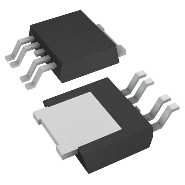
P-TO252-5-11
Functional Description
The TLE 4476 is a monolithic integrated voltage regulator providing two output voltages,
Q1 is a 3.3 V output for loads up to 350 mA and Q2 is a 5 V output providing 430 mA.
The device is available in the PG-TO252-5-11 (D-Pak) package. Output 2 can be
switched ON/OFF via the Enable input EN.
The TLE 4476 is designed to supply microprocessor systems under the severe
conditions of automotive applications and is therefore equipped with additional
protection functions against overload, short circuit and overtemperature.
Type
Package
TLE 4476 D
PG-TO252-5-11
Data Sheet
1
Rev. 2.5, 2007-03-20
�TLE 4476
PG-TO252-5
GND
1
5
Ι
EN
Q1
Q2
AEP02562
Figure 1
Pin Configuration (top view)
Table 1
Pin Definitions and Functions
Pin No.
Symbol
Function
1
I
Input voltage; block to GND directly at the IC with a
ceramic capacitor
2
Q1
3.3 V output; block to GND with a capacitor CQ1 ≥ 10 μF,
ESR < 2 Ω at 10 kHz
3
GND
Ground
4
Q2
5.0 V output; block to GND with a capacitor CQ2 ≥ 10 μF,
ESR < 3 Ω at 10 kHz
5
EN
Enable input; to switch ON and OFF Q2, ON with high
signal
Data Sheet
2
Rev. 2.5, 2007-03-20
�TLE 4476
Ι
1
2
Q1
Bandgap
Reference
4
EN
Q2
5
3
GND
Figure 2
Data Sheet
AEB02563
Block Diagram
3
Rev. 2.5, 2007-03-20
�TLE 4476
Table 2
Absolute Maximum Ratings
-40 °C < Tj < 170 °C
Parameter
Symbol
Limit Values
Unit
Remarks
–
Min.
Max.
-42
–
42
65
V
V
t < 400 ms
II
–
–
mA
Internally limited
VQ1
IQ1
-1
36
V
–
–
–
mA
Internally limited
VQ2
IQ2
-1
36
V
–
–
–
mA
Internally limited
VEN
-42
–
42
65
V
V
–
t < 400 ms
IEN
–
–
mA
Internally limited
Tj
Tstg
-50
170
°C
–
-50
150
°C
–
Input I
Voltage
Current
VI
3.3 V Output Q1
Voltage
Current
5.5 V Output Q2
Voltage
Current
Inhibit EN
Voltage
Current
Temperatures
Junction temperature
Storage temperature
Notes
1. ESD-Protection according to MIL Std. 883: ±2 kV.
2. Stresses above those listed here may cause permanent damage to the device.
Exposure to absolute maximum rating conditions for extended periods may affect
device reliability.
Data Sheet
4
Rev. 2.5, 2007-03-20
�TLE 4476
Table 3
Operating Range
Parameter
Symbol
Limit Values
Unit
Remarks
Min.
Max.
VI1
VI1
IO1
4.5
42
V
1)
5.7
42
V
2)
0
350
mA
–
5 V regulator
output current
IO2
0
430
mA
–
Junction temperature
Tj
-40
170
°C
3)
Rth,j-case
Rth,j-a
–
3
K/W
–
–
80
K/W
4)
Output 1 input voltage
Output 2 input voltage
3.3 V regulator
output current
Thermal Resistances
Junction case
Junction ambient
1) Input voltage VI required for operation of output Q1
2) Input voltage VI required for operation of output Q2
3) The overtemperature protection is set to > 170 °C. The voltage regulator may not be operated continuously at
170 °C as device reliability will be reduced to 500 h statistic lifetime.
4) Worst case regarding peak temperature, zero airflow; mounted on a PCB 80 × 80 × 1.5 mm3, 35 μm Cu,
5 μm Sn, heat sink area 300 mm2.
Note: In the operating range the functions given in the circuit description are fulfilled.
Data Sheet
5
Rev. 2.5, 2007-03-20
�TLE 4476
Table 4
Electrical Characteristics
VI = 13.5 V; VEN > VENH; -40 °C < Tj < 150 °C; unless otherwise specified.
Parameter
Symbol
Limit Values
Unit
Test Condition
Min. Typ. Max.
3.3 V Output Q1
VQ1
IQ1
ΔVQ1
ΔVQ1
3.17 3.3
3.43
V
1 mA < IQ1 < 250 mA
350
–
900
mA
1)
–
–
30
mV
1 mA < IQ1 < 250 mA
–
–
20
mV
Power Supply Ripple
Rejection
PSRR
–
60
–
dB
IQ1 = 5 mA;
6 V < VI < 28 V
20 Hz < fr < 20 kHz2);
Vr = 5 Vpp
Output capacitor
CQ1
RESRQ1
10
–
–
μF
–
–
–
2
Ω
at 10 kHz
VQ2
IQ2
VDRQ2
4.8
5.0
5.2
V
1 mA < IQ2 < 330 mA
430
–
900
mA
1)
–
0.3
0.7
V
IQ2 = 330 mA1)
Load regulation
ΔVQ2
–
–
50
mV
5 mA < IQ2 < 330 mA
Line regulation
ΔVQ2
–
–
50
mV
Power Supply Ripple
Rejection
PSRR
–
60
–
dB
IQ2 = 5 mA;
6 V < VI < 28 V
20 Hz < fr < 20 kHz2);
Vr = 5 Vpp
Output capacitor
CQ2
RESRQ2
10
–
–
μF
–
–
–
3
Ω
at 10 kHz
Output voltage
Output current limitation
Load regulation
Line regulation
ESR of output capacitor
5.0 V Output Q2
Output voltage
Output current limitation
Drop voltage;
VDRQ2 = VI - VQ2
ESR of output capacitor
Data Sheet
6
Rev. 2.5, 2007-03-20
�TLE 4476
Table 4
Electrical Characteristics (cont’d)
VI = 13.5 V; VEN > VENH; -40 °C < Tj < 150 °C; unless otherwise specified.
Parameter
Symbol
Limit Values
Unit
Test Condition
Tj < 85 °C;
VEN = 0 V
IQ1 = IQ2 = 300 μA;
Tj < 85 °C
IQ1 = 150 mA;
IQ2 = 300 μA
IQ1 = 300 μA;
IQ2 = 250 mA
Min. Typ. Max.
Current Consumption
Quiescent current;
Iq = II - IQ1
Iq
–
100
150
μA
Quiescent current;
Iq = II - IQ1 - IQ2
Iq
–
300
400
μA
Quiescent current;
Iq = II - IQ1 - IQ2
Iq
–
2.5
10
mA
Quiescent current;
Iq = II - IQ2 - IQ1
Iq
–
5
13
mA
VEN ON
VEN OFF
VEN
1.8
–
–
V
–
–
1.0
V
–
20
30
μA
Enable Input EN
EN ON voltage
EN OFF voltage
Input current
VQ2 ON
VQ2 OFF
VEN = 13 V
1) Measured when the output voltage VQ has dropped 100 mV from the nominal value.
2) Guaranteed by design.
Data Sheet
7
Rev. 2.5, 2007-03-20
�TLE 4476
Application Information
Ι
5.7 - 42 V
Q1
CΙ
470 nF
3.3 V
C Q1
22 μF
Bandgap
Reference
Q2
5V
C Q2
22 μF
e.g. from
Ignition
EN
GND
AES02564
Figure 3
Application Circuit
Input, Output
The input capacitor CI is necessary for compensating line influences. Using a resistor of
approx. 1 Ω in series with CI, the LC circuit of input inductivity and input capacitance can
be damped. To stabilize the regulation circuits of the stand-by and main regulator, output
capacitors CQ1 and CQ2 are necessary. Stability is guaranteed at values CQ1 ≥ 10 μF
(ESR ≤ 2 Ω) and CQ2 ≥ 10 μF (ESR ≤ 3 Ω) within the operating temperature range.
Enable
Using the enable feature the output 2 (5 V output) can be switched ON or OFF. The
enable input can be connected directly to terminal 30 (battery line) or 15 (ignition line). It
is also possible to control the output 2 via the microcontroller.
Data Sheet
8
Rev. 2.5, 2007-03-20
�TLE 4476
Typical Performance Characteristics
Output Current IQ1 versus
Input Voltage VI
Output Current IQ2 versus
Input Voltage VI Enable ON
AED02844
1200
mA
I Q2
I Q1
800
800
600
600
400
400
200
200
0
AED02845
1200
mA
0
10
20
30
0
40 V 50
0
10
20
30
VI
VI
Output Voltage VQ2
versus Temperature Tj
Output Voltage VQ1
versus Temperature Tj
AED03039
5.2
VQ2
AED03040
3.5
VQ1
V
5.1
V
3.4
Q1
Q2
5.0
3.3
4.9
3.2
4.8
-40
0
40
80
3.1
-40
120 ˚C 160
Tj
Data Sheet
40 V 50
0
40
80
120 ˚C 160
Tj
9
Rev. 2.5, 2007-03-20
�TLE 4476
Drop Voltage VDR1 versus
Output Current IQ1
Drop Voltage VDR2 versus
Output Current IQ2 EN ON
AED02847
1200
mV
VDR1
VDR2
AED02848
600
mV
500
800
400
600
300
400
200
200
100
0
0
50
100
150
0
200 mA 250
0
100
200
300
I Q1
I Q2
Current Consumption Iq
versus Input Voltage VI
Iq
Current Consumption Iq
versus Input Voltage VI
AED02849
6
mA
400 mA 500
Iq
AED02846
6
mA
5
5
4
4
R L2 = 50 Ω
3
3
2
2
R L2 = 100 Ω
1
1
0
R L1 = 33 Ω
R L1 = 330 Ω
R L1 = 3.3 k Ω
0
10
20
30
0
40 V 50
10
20
30
40 V 50
VI
VI
Data Sheet
0
10
Rev. 2.5, 2007-03-20
�TLE 4476
Current Consumption Iq
versus Output Current IQ1
Current Consumption Iq
versus Output Current IQ2
AED02850
20
AED02851
30
Iq mA
Iq mA
25
10
20
15
5
10
5
0
0
50
100
150
0
200 mA 250
0
100
200
300 mA 400
I Q1
I Q2
Output Voltage VQ1 versus
Input Voltage VI
Output Voltage VQ2 versus
Input Voltage VI
AED02852
6
VQ1 V
VQ2 V
5
5
4
4
3
3
2
2
1
1
0
0
5
10
15
0
20 V 25
VI
Data Sheet
AED02853
6
0
5
10
15
20 V 25
VI
11
Rev. 2.5, 2007-03-20
�TLE 4476
Package Outlines
6.5 +0.15
-0.05
A
1)
2.3 +0.05
-0.10
B
(5)
0.51 MIN.
0.15 MAX.
per side
0.5 +0.08
-0.04
0.9 +0.20
-0.01
0...0.15
0.8 ±0.15
(4.24) 1 ±0.1
9.98 ±0.5
6.22 -0.2
5.7 MAX.
5 x 0.6 ±0.1
0.5 +0.08
-0.04
1.14
4.56
0.1 B
0.25 M A B
1) Includes mold flashes on each side.
All metal surfaces tin plated, except area of cut.
GPT09527
Figure 4
PG-TO252-5-11 (Plastic Transistor Single Outline)
Green Product (RoHS compliant)
To meet the world-wide customer requirements for environmentally friendly products
and to be compliant with government regulations the device is available as a green
product. Green products are RoHS-Compliant (i.e Pb-free finish on leads and suitable
for Pb-free soldering according to IPC/JEDEC J-STD-020).
You can find all of our packages, sorts of packing and others in our
Infineon Internet Page “Products”: http://www.infineon.com/products.
Dimensions in mm
SMD = Surface Mounted Device
Data Sheet
12
Rev. 2.5, 2007-03-20
�TLE 4476
Revision History
Version
Date
Changes
Rev. 2.5
2007-03-20
Initial version of RoHS-compliant derivate of TLE 4476
Page 1: AEC certified statement added
Page 1 and Page 12: RoHS compliance statement and
Green product feature added
Page 1 and Page 12: Package changed to RoHS compliant
version
Legal Disclaimer updated
Data Sheet
13
Rev. 2.5, 2007-03-20
�Edition 2007-03-20
Published by
Infineon Technologies AG
81726 Munich, Germany
© 2007 Infineon Technologies AG
All Rights Reserved.
Legal Disclaimer
The information given in this document shall in no event be regarded as a guarantee of conditions or
characteristics. With respect to any examples or hints given herein, any typical values stated herein and/or any
information regarding the application of the device, Infineon Technologies hereby disclaims any and all warranties
and liabilities of any kind, including without limitation, warranties of non-infringement of intellectual property rights
of any third party.
Information
For further information on technology, delivery terms and conditions and prices, please contact the nearest
Infineon Technologies Office (www.infineon.com).
Warnings
Due to technical requirements, components may contain dangerous substances. For information on the types in
question, please contact the nearest Infineon Technologies Office.
Infineon Technologies components may be used in life-support devices or systems only with the express written
approval of Infineon Technologies, if a failure of such components can reasonably be expected to cause the failure
of that life-support device or system or to affect the safety or effectiveness of that device or system. Life support
devices or systems are intended to be implanted in the human body or to support and/or maintain and sustain
and/or protect human life. If they fail, it is reasonable to assume that the health of the user or other persons may
be endangered.
�
很抱歉,暂时无法提供与“TLE4476DATMA1”相匹配的价格&库存,您可以联系我们找货
免费人工找货