Dual Voltage Regulator with 5 V and 15 V Outputs
TLE 4484
Features
•
•
•
•
•
•
•
•
•
Dual output: 5 V and 15 V
High input voltage range: up to 45 V
High output current capability
High output voltage accuracy
Very low current consumption
Short circuit protected
Overtemperature protected
Thermal and space optimized package
Industrial type
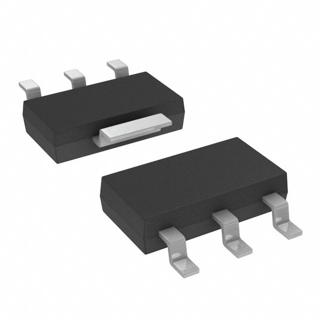
P-SOT223-4
Functional Description
The TLE 4484 G is a monolithic integrated voltage regulator providing two output
voltages, output Q5 is a 5 V output for loads up to 25 mA and output Q15 is a 15 V output
providing up to 30 mA. The device is based on the Infineon double isolated bipolar
technology DOPL with high accuracy polysilicon resistors and is available in the
P-SOT223-4-2 package.
The TLE 4484 G is designed to supply systems with a microcontroller (5 V) and a
standard MOS-driver-IC (15 V) under severe conditions and is therefore equipped with
additional protection functions.
Both outputs are protected against overload, short circuit to ground and to the input
voltage. A build-in shutdown-circuit protects the device against overheat.
The IC operates in a wide input voltage range up to 45 V. The output voltages are
regulated to VQ5 = 5 V and VQ15 = 15 V with a drop voltage less than 1.5 V. The standard
P-SOT223-4-2 package is especially suitable for this kind of application, saves PCBboard-space and reduces system cost.
Type
Ordering Code
Package
TLE 4484 G
Q67006-A9396
P-SOT223-4-2
Data Sheet
1
Rev. 1.0, 2004-01-01
�TLE 4484
GND
4
1
2
I
Q5
3
Q15
AEP02857
Figure 1
Pin Configuration (top view)
Table 1
Pin Definitions and Functions
Pin No.
Symbol
Function
1
I
Input voltage; block to ground directly at the IC with a
ceramic capacitor.
2
Q5
Output voltage for microcontroller and logic circuit;
block to ground with a ceramic capacitor.
3
Q15
Output voltage for MOS driver circuit; block to ground with
a ceramic capacitor.
4
GND
Ground
Data Sheet
2
Rev. 1.0, 2004-01-01
�TLE 4484
I
Q5
Overcurrent
Protection
Buffer
Reference
1.25 V
Thermal
Protection
Q15
Overcurrent
Protection
Buffer
Reference
1.25 V
GND
AEB02862
Figure 2
Data Sheet
Block Diagram
3
Rev. 1.0, 2004-01-01
�TLE 4484
Table 2
Absolute Maximum Ratings
Parameter
Symbol
Limit Values
Unit
Remarks
Min.
Max.
VI
II
-0.3
45
V
–
–
–
–
internally limited
VQ5
IQ5
-1
45
V
VQ5 < VI
–
–
–
internally limited
VQ15
IQ15
-1
45
V
VQ15 < VI
–
–
–
internally limited
IGND
-5
5
mA
–
Tj
Tstg
-50
150
°C
1)
-50
150
°C
–
-2
2
kV
Input
Voltage
Current
Output Q5
Voltage
Current
Output Q15
Voltage
Current
GND
Current
Temperatures
Junction temperature
Storage temperature
ESD-Protection (Human Body Model)
All pins
VESD
1) The overtemperature protection will be set to 150 °C min. The voltage regulator should not be operated
continuously at 170 °C as device reliability will be reduced to 500 h.
Attention: Stresses above those listed here may cause permanent damage to the
device. Exposure to absolute maximum rating conditions for extended
periods may affect device reliability.
Data Sheet
4
Rev. 1.0, 2004-01-01
�TLE 4484
Table 3
Operating Range
Parameter
Output Q5 input voltage
Output Q15 input voltage
Junction temperature
Symbol
Limit Values
Unit
Remarks
Min.
Max.
VI1
VI1
Tj
6.5
45
V
–
16.5
45
V
–
-40
150
°C
–
Rth,j-a
–
165
K/W
zero airflow, zero
heat sink area
Thermal Resistances
Junction ambient
Note: In the operating range, the functions given in the circuit description are fulfilled.
Data Sheet
5
Rev. 1.0, 2004-01-01
�TLE 4484
Table 4
Electrical Characteristics
17 V < VI < 42 V; -40 °C < Tj < 125 °C; all voltages with respect to ground; positive current
defined flowing out of pin; unless otherwise specified.
Parameter
Symbol
Limit Values
Min.
Typ.
Max.
Unit
Test Condition
IQ5 = 1 mA;
IQ15 = 1 mA
IQ5 = 25 mA;
IQ15 = 30 mA
Current Consumption
Quiescent current;
Iq = II - (IQ5 + IQ15)
Iq
–
450
550
µA
Quiescent current;
Iq = II - (IQ5 + IQ15)
Iq
–
0.76
1
mA
VQ5
4.85
5.00
5.15
V
4.75
–
5.25
V
16
40
–
mA
1)
30
–
–
mA
–
0.9
1.5
V
Tj = 25 °C
IQ5 = 25 mA1)
–
25
50
mV
1 mA < IQ5 < 25 mA;
VI = 17 V
IQ5 = 1 mA;
7 V < VI < 27 V
20 Hz < fr < 20 kHz;
Vr = 5 Vpp
5-V Output Q5
Output voltage
VQ5
Output current limitation IQ5
Output current limitation IQ5
VDRQ5
Output drop voltage;
VDRQ5 = VI - VQ5
Load regulation
∆VQ5
Output voltage
IQ5 = 10 mA;
Tj = 25 °C
1 mA < IQ5 < 25 mA
Line regulation
∆VQ5
–
20
50
mV
Power Supply Ripple
Rejection
PSRR5
–
50
–
dB
Value of output cap.
CQ5
RESRQ5
1.0
–
–
µF
–
–
–
2.0
Ω
–
VQ15
14.4
15.0
15.6
V
IQ15 = 15 mA;
Tj = 25 °C
1 mA < IQ15 < 30 mA
ESR of output cap.
15 V Output Q15
Output voltage
VQ15
Output current limitation IQ15
Output drop voltage;
VDRQ15
VDRQ15 = VI - VQ15
Load regulation
∆VQ15
Output voltage
Data Sheet
14.25 –
15.75 V
40
–
–
mA
1)
–
0.9
1.5
V
IQ15 = 30 mA1)
–
10
50
mV
1 mA < IQ15 < 30 mA;
VI = 17 V
6
Rev. 1.0, 2004-01-01
�TLE 4484
Table 4
Electrical Characteristics (cont’d)
17 V < VI < 42 V; -40 °C < Tj < 125 °C; all voltages with respect to ground; positive current
defined flowing out of pin; unless otherwise specified.
Parameter
Symbol
Limit Values
Min.
Typ.
Max.
Unit
Test Condition
IQ15 = 5 mA;
16 V < VI < 36 V
20 Hz < fr < 20 kHz;
Vr = 5 Vpp
Line regulation
∆VQ15
–
80
150
mV
Power Supply Ripple
Rejection
PSRR15 –
50
–
dB
Value of output cap.
CQ15
1.0
RESRQ15 –
–
–
µF
–
–
4.0
Ω
–
ESR of output cap.
1) Measured when the output voltage VQ has dropped 100 mV from the nominal value.
Note: The listed characteristics are ensured over the operating range of the integrated
circuit. Typical characteristics specify mean values expected over the production
spread. If not otherwise specified, typical characteristics apply at TA = 25 °C and
the given supply voltage.
Data Sheet
7
Rev. 1.0, 2004-01-01
�TLE 4484
Supply
22 nF
I
Q5
10 µF
CQ5
Overcurrent
Protection
VQ5
Buffer
Reference
1.25 V
Thermal
Protection
Q15
CQ15
Overcurrent
Protection
VQ15
Buffer
Reference
1.25 V
GND
AES02863
Figure 3
Data Sheet
Application Circuit
8
Rev. 1.0, 2004-01-01
�TLE 4484
Typical Performance Characteristics
Output Voltage VQ5 and VQ15
versus Input Voltage VI
VQ
Output Current Limit IQ5 and IQ15
versus Junction Temperature Tj
AED02858
32
V
28
IQ
AED02861
140
mA
120
24
Q15
100
20
80
VQ15
16
60
12
40
8
Q5
VQ5
20
4
0
0
4
8
12
16
0
-50 -25
20 V 24
0
25 50 75 100
˚C 150
TI
VI
Current Consumption Iq
versus Junction Temperature Tj
Iq
AED02859
600
µA
VI = 42 V
480
420
VI = 17 V
360
300
240
180
120
60
0
-50 -25
0
25 50 75 100
˚C 150
Tj
Data Sheet
9
Rev. 1.0, 2004-01-01
�TLE 4484
Package Outlines
1.6 ±0.1
6.5 ±0.2
0.1 MAX.
2
B
0.5 MIN.
1
+0.2
acc. to
DIN 6784
3.5 ±0.2
4
7 ±0.3
3 ±0.1
15˚ MAX.
A
3
0.28 ±0.04
2.3
0.7 ±0.1
4.6
0.25
M
A
0.25
M
B
GPS05560
Figure 4
P-SOT223-4-2 (Plastic Small Outline Transistor)
You can find all of our packages, sorts of packing and others in our
Infineon Internet Page “Products”: http://www.infineon.com/products.
Dimensions in mm
SMD = Surface Mounted Device
Data Sheet
10
Rev. 1.0, 2004-01-01
�Edition 2004-01-01
Published by Infineon Technologies AG,
St.-Martin-Strasse 53,
81669 München, Germany
© Infineon Technologies AG 2004.
All Rights Reserved.
Attention please!
The information herein is given to describe certain components and shall not be considered as a guarantee of
characteristics.
Terms of delivery and rights to technical change reserved.
We hereby disclaim any and all warranties, including but not limited to warranties of non-infringement, regarding
circuits, descriptions and charts stated herein.
Information
For further information on technology, delivery terms and conditions and prices please contact your nearest
Infineon Technologies Office (www.infineon.com).
Warnings
Due to technical requirements components may contain dangerous substances. For information on the types in
question please contact your nearest Infineon Technologies Office.
Infineon Technologies Components may only be used in life-support devices or systems with the express written
approval of Infineon Technologies, if a failure of such components can reasonably be expected to cause the failure
of that life-support device or system, or to affect the safety or effectiveness of that device or system. Life support
devices or systems are intended to be implanted in the human body, or to support and/or maintain and sustain
and/or protect human life. If they fail, it is reasonable to assume that the health of the user or other persons may
be endangered.
�
很抱歉,暂时无法提供与“TLE4484G”相匹配的价格&库存,您可以联系我们找货
免费人工找货