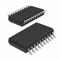
Data Sheet TLE 6225 G
Smart Quad Low-Side Switch
Features
• Shorted circuit protection
• Overtemperature protection
• Overvoltage protection
• Open Load Detection
• Direct parallel control of the inputs
• Inputs high or low active programmable
• General fault flag
• Very low standby quiescent current
• Compatible with 3V microcontrollers
• Electostatic discharge (ESD) protection
Product Summary
Supply voltage
Drain source voltage
On resistance
Output current(each)
(individ.)
VS
VDS(AZ)max
RON
ID(NOM)
Application
• µC compatible power switch for 12 V applications
• Switch for automotive and industrial systems
• Line, relay or lamp driver
4.5 – 32
V
60
V
1.7
Ω
350
mA
500
mA
P-DSO 20-6
Ordering Code:
Q 67006 A9373
General description
Quad channel Low-Side Switch in Smart Power Technology (SPT) with four separate inputs
and four open drain DMOS output stages. The TLE 6225 G is protected by embedded protection functions and designed for automotive and industrial applications, to drive lines, lamps
and relays.
Block Diagram
PRG
GND
ENA
VS
FAULT
VS
Diagnostic,
Protection
IN1
Vbb
Over Temp.
as Ch. 1
Logic
Open Load
as Ch. 1
Output Stage
IN4
OUT1
as Ch. 1
1
4
Output Control
Buffer
4
OUT4
GND
Page
1
05.December 2000
�Data Sheet TLE 6225 G
Pin Description
Pin
1
2
3
4
5
6
7
8
9
10
11
12
13
14
15
16
17
18
19
20
Symbol
IN1
IN2
FAULT
GND
GND
GND
GND
VS
IN3
IN4
ENA
OUT4
OUT3
GND
GND
GND
GND
OUT2
OUT1
PRG
Pin Configuration (Top view)
Function
Input Channel 1
Input Channel 2
General Fault Flag
Ground
Ground
Ground
Ground
Supply Voltage
Input Channel 3
Input Channel 4
Enable for all channels/Standby
Power Output channel 4
Power Output channel 3
Ground
Ground
Ground
Ground
Power Output channel 2
Power Output channel 1
Program (inputs high or low active)
Page
2
IN1
IN2
FAULT
GND
GND
GND
GND
VS
IN3
IN4
1•
2
3
4
5
6
7
8
9
10
20
19
18
17
16
15
14
13
12
11
PRG
OUT1
OUT2
GND
GND
GND
GND
OUT3
OUT4
ENA
P-DSO-20-6
05.December 2000
�Data Sheet TLE 6225 G
Maximum Ratings for Tj = – 40°C to 150°C
Parameter
Symbol
Values
Supply Voltage
VS
-0.3 ... +40
V
Continuous Drain Source Voltage (OUT1...OUT4)
VDS
-0.7 ... +45
V
Input Voltage, IN1 - IN4
VIN
- 0.3 ... + 7
V
Input Voltage, PRG, ENA
VIN
- 0.3 ... + 40
V
75
V
2)
Unit
Output Load Dump Protection VLoad Dump=UP+US; UP=13.5 V
With Automotive Relay Load RL = 70 Ω
RI1)=2 Ω; td=400ms; IN = low or high
VLoad Dump
FAULT Output Voltage
VFault
- 0.3 ... + 40
V
Operating Temperature Range
Storage Temperature Range
Tj
Tstg
- 40 ... + 150
- 55 ... + 150
°C
Output Current per Channel (see electrical characteristics)
ID(lim)
self limited
A
EAS
10
mJ
Power Dissipation (DC) @ TA = 25 °C (on PCB 6 cm cooling area)
Ptot
2.5
W
Electrostatic Discharge Voltage (Human Body Model)
according to MIL STD 883D, method 3015.7 and EOS/ESD
assn. standard S5.1 - 1993
VESD
2000
V
Output Clamping Energy
ID= 0.2 A
2
DIN Humidity Category, DIN 40 040
E
IEC Climatic Category, DIN IEC 68-1
40/150/56
Thermal Resistance
junction - pin
junction - ambient @ min. footprint
junction - ambient @ 6 cm2 cooling area
1)
2)
23
80
45
RthJP
RthJA
RthJA
K/W
RI=internal resistance of the load dump test pulse generator LD200
VLoadDump is setup without DUT connected to the generator per ISO 7637-1 and DIN 40 839.
Page
3
05.December 2000
�Data Sheet TLE 6225 G
Electrical Characteristics
Parameter and Conditions
VS = 4.5 to 32 V ; Tj = - 40 °C to + 150 °C
(unless otherwise specified)
Symbol
Values
min
typ
Unit
max
1. Power Supply
Supply Voltage
VS
Supply Current (ENA = H, Outputs ON)
IS(ON)
Supply Current in Standby Mode (ENA = L)
IS(stby)
32
V
2
mA
10
µA
1.7
3
2
3.6
Ω
45
50
60
V
500
750
1000
mA
5
µA
4.5
1
2. Power Outputs
ON Resistance VS ≥ 6 V; ID = 300 mA
Output Clamping Voltage
TJ = 25°C
TJ = 150°C
RDS(ON)
Output OFF
VDS(AZ)
Current Limit
Output Leakage Current
ID(lim)
VENA = L
ID(lkg)
Turn-On Time
ID = 200 mA, resistive load
tON
5
10
µs
Turn-Off Time
ID = 200 mA, resistive load
tOFF
5
10
µs
3. Digital Inputs (IN1 – IN4, ENA, PRG)
Input Low Voltage (IN1 – IN4, PRG)
VINL
- 0.3
1
V
Input Low Voltage (ENA)
VINL
- 0.3
0.8
V
Input High Voltage
VINH
2.0
Input Voltage Hysteresis (IN1 – IN4, PRG)
VINHys
50
100
mV
Input Voltage Hysteresis (ENA)
VINHys
20
100
mV
Input Pull Up Current (IN1...IN4) @ PRG = L,
VIN = 0V
IIN(1..4)PU
20
50
100
µA
Input Pull Down Current (IN1...IN4) @ PRG = H,
VIN < VS; VIN < 6
IIN(1..4)PD
20
50
100
µA
PRG, ENA Pull Down Current
VIN = 5 V
IIN(PRG,ENA)
20
50
100
µA
PRG, ENA Pull Down Current
VIN = 14 V
IIN(PRG,ENA)
200
µA
VFAULTL
0.4
V
Open Load/Short to Ground Detection Voltage
VDS(OL)
0.4*VS 0.5*VS 0.6*VS
V
Output Pull Down Current
IPD(OL)
20
50
200
µA
Fault Delay Time; VS = 12V
td(fault)
50
100
200
µs
Overtemperature Shutdown Threshold
Hysteresis
Tth(sd)
Thys
170
200
°C
K
V
4. Digital Output ( FAULT )
FAULT Output Low Voltage
IFAULT = 1.6 mA
5. Diagnostic Functions
Page
4
10
05.December 2000
�Data Sheet TLE 6225 G
Functional Description
The TLE 6225 G is a quad channel low-side switch with four power DMOS stages. The power
transistors are protected against short to VBB, overload, overtemperature and against overvoltage by zenerclamp.
The diagnostic logic recognises a fault condition which is indicated by a fault flag.
Circuit Description
Output Stage Control
Each output is independently controlled by an input pin and a common enable line, which enables/disables all four outputs. The parallel inputs are high or low active depending on the
PRG pin. If the parallel input pins are not connected (independent of high or low activity) it is
guaranteed that the outputs 1 to 4 are switched OFF. ENA - and PRG - pin itself are internally
pulled down when they are not connected.
ENA - Enable pin.
ENA = High:
Active mode. Channels are enabled
ENA = Low (GND): Sleep mode. Channels are switched off. Less than
1 µA current consumption.
PRG - Program pin.
PRG = High:
Parallel inputs Channel 1 to 4 are high active
PRG = Low (GND): Parallel inputs Channel 1 to 4 are low active.
Power Transistors
Each of the four output stages has its own zenerclamp. This causes a voltage limitation at the
power transistors when inductive loads are switched off. The outputs are provided with a current limitation set to a minimum of 500 mA.
Each output is protected by embedded protection functions. In the event of an overload or
short to supply, the current is internally limited. If this operation leads to an overtemperature
condition, a second protection level (about 170 °C) will turn the effected output into a PWMmode (selective thermal shutdown with restart) to prevent critical chip temperatures. The temperature hysteresis is typically 10K.
Diagnostic
The FAULT pin is an open drain output. The logic status depends on the programming pin
PRG.
FAULT - pin.
FAULT = High
FAULT = Low
no fault @ PRG = High
no fault @ PRG = Low
Page
5
05.December 2000
�Data Sheet TLE 6225 G
Diagnostic Table
Enable
Input
Program
Input
Control
Input
Power
Output
Diagnostic
Output
ENA
PRG
IN
OUT
FAULT
Standby
L
X
X
OFF
H
Normal function
H
H
H
H
L
L
H
H
L
H
L
H
ON
OFF
OFF
ON
L
L
H
H
Overtemperature
H
H
L
H
L
H
OFF *
OFF *
H
L
Open load or short to ground
H
H
H
H
L
L
H
H
L
H
L
H
ON
OFF
OFF
ON
L
H
L
H
Operating Condition
X = not relevant
*selective thermal shutdown for each channel at overtemperature
Fault Distinction
Open load/short to ground is recognised in OFF-state. Overtemperature as a result of an
overload or short to battery can only arise in ON-state. If there is only one fault at a time, it is
possible to distinguish which channel is affected with which fault.
Page
6
05.December 2000
�Data Sheet TLE 6225 G
Typical electrical Characteristics
Drain-Source on-resistance
RDS(ON) = f (Tj) ; Vs = 5V
Channel 1-4
Typical Drain- Source ON-Resistance
3,5
RDS(ON) [Ohm]
3
2,5
2
1,5
1
-50
-25
0
25
50
75
100
125
150
175
Tj[°C]
Figure 6 :
Typical ON Resistance versus Junction-Temperature
Channel 1-4
Output Clamping Voltage
VDS(AZ) = f (Tj) ; Vs = 5V
Channel 1-4
Typical Clamping Voltage
55
54
VDS (AZ) [V]
53
52
51
50
49
48
-50
-25
0
25
50
75
100
125
150
175
Tj[°C]
Figure 7 :
Typical Clamp Voltage versus Junction-Temperature
Channel 1-4
Page
7
05.December 2000
�Data Sheet TLE 6225 G
Timing Diagrams
Power Outputs
VIN
t
tOFF
tON
VDS
80%
20%
t
Application Circuit
VBB
+5V
VS
PRG
VCC
TLE
6225 G
Py.1
ENA
Px.1
IN1
OUT1
Px.2
µC
e.g. C166 Px.3
IN2
OUT2
IN3
OUT3
IN4
OUT4
Px.4
INT
+5V
Line
FAULT
GND
Page
8
05.December 2000
�Data Sheet TLE 6225 G
Package and ordering code
all dimensions in mm
P - DSO - 20 - 6
TLE 6225 G
Ordering code
1.27
0.35 +0.15
8˚ ma
+0.09
7.6 -0.21)
x
0.35 x 45˚
0 .2 3
2.65 max
2.45 -0.2
0.2 -0.1
Q 67006 A9373
0.4 +0.8
2)
0.2 24x
20
0.1
10.3 ±0.3
11
1 12.8 1) 10
-0.2
GPS05094
Index Marking
1) Does not include plastic or metal protrusions of 0.15 max per side
2) Does not include dambar protrusion of 0.05 max per side
Published by
Infineon Technologies AG,
Bereichs Kommunikation
St.-Martin-Strasse 76,
D-81541 München
© Infineon Technologies AG 1999
All Rights Reserved.
Attention please!
The information herein is given to describe certain components and shall not be considered as warranted characteristics.
Terms of delivery and rights to technical change reserved.
We hereby disclaim any and all warranties, including but not limited to warranties of non-infringement, regarding circuits,
descriptions and charts stated herein.
Infineon Technologies is an approved CECC manufacturer.
Information
For further information on technology, delivery terms and conditions and prices please contact your nearest Infineon Technologies Office in Germany or our Infineon Technologies Representatives worldwide (see address list).
Warnings
Due to technical requirements components may contain dangerous substances. For information on the types in question
please contact your nearest Infineon Technologies Office.
Infineon Technologies Components may only be used in life-support devices or systems with the express written approval of
Infineon Technologies, if a failure of such components can reasonably be expected to cause the failure of that life-support
device or system, or to affect the safety or effectiveness of that device or system. Life support devices or systems are intended to be implanted in the human body, or to support and/or maintain and sustain and/or protect human life. If they fail, it
is reasonable to assume that the health of the user or other persons may be endangered.
Page
9
05.December 2000
�
很抱歉,暂时无法提供与“TLE6225G”相匹配的价格&库存,您可以联系我们找货
免费人工找货