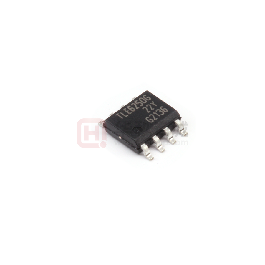
TLE6250
Hi gh Speed CAN-Transceiver
Features
•
CAN data transmission rate up to 1 Mbit/s
•
Receive-only mode and Stand-by mode
•
Suitable for 12 V and 24 V applications
•
Excellent EMC performance (very high immunity and very low emission)
•
Versions for 5 V and 3.3 V microcontrollers
•
Bus pins are short circuit proof to ground and battery voltage
•
Overtemperature protection
•
Very wide temperature range (-40°C up to 150°C)
•
Green Product (RoHS compliant)
Potential applications
•
Engine control unit (ECUs)
•
Transmission control units (TCUs)
•
Chassis control modules
•
Electric power steering
Product validation
Qualified for automotive applications. Product validation according to AEC-Q100.
Description
The HS CAN-transceivers of the TLE6250 family are monolithic integrated circuits that are available as bare die
as well as in a PG-DSO-8 package with the same functionality. The transceivers are optimized for high speed
differential mode data transmission in automotive applications and industrial applications and they are
compatible to ISO 11898. The transceivers work as an interface between the CAN protocol controller and the
physical differential bus in both 12 V systems and 24 V systems.
The transceivers are based on the Smart Power Technology (SPT), which allows bipolar and CMOS control
circuitry in accordance with DMOS power devices to coexist in the monolithic circuit. The TLE6250 is designed
to withstand the severe conditions of automotive applications and provides excellent EMC performance.
TLE6250G
5 V logic I/O version: RxD, TxD, INH, RM. Two control pins (RM, INH) and three operation modes: Normal mode,
Stand-by mode and Receive-only mode.
Datasheet
www.infineon.com/automotive-transceivers
1
Rev. 4.2
2022-02-03
�TLE6250
High Speed CAN-Transceiver
The functions and parameters of the TLE6250G and TLE6250C are identical, except those related to the
package. In this document the content for TLE6250G also applies to TLE6250C, unless otherwise stated.
TLE6250GV33
3.3 V logic I/O version (logic I/O voltage adaptive to V33V pin in the range of 3.3 V to 5 V): RxD, TxD, INH. One
control pin (INH) and two operation modes: Normal mode and Standby mode.
The functions and parameters of theTLE6250GV33 and TLE6250CV33 are identical, except those related to the
package. In this document the content for TLE6250GV33 also applies to TLE6250CV33, unless otherwise
stated.
Type
Package
Marking
TLE6250G
PG-DSO-8
TLE6250
TLE6250C
(chip)
–
TLE6250GV33
PG-DSO-8
625033
TLE6250CV33
(chip)
–
Datasheet
2
Rev. 4.2
2022-02-03
�TLE6250
High Speed CAN-Transceiver
Table of contents
Features . . . . . . . . . . . . . . . . . . . . . . . . . . . . . . . . . . . . . . . . . . . . . . . . . . . . . . . . . . . . . . . . . . . . . . . . 1
Potential applications . . . . . . . . . . . . . . . . . . . . . . . . . . . . . . . . . . . . . . . . . . . . . . . . . . . . . . . . . . . . . 1
Product validation . . . . . . . . . . . . . . . . . . . . . . . . . . . . . . . . . . . . . . . . . . . . . . . . . . . . . . . . . . . . . . . . 1
Description . . . . . . . . . . . . . . . . . . . . . . . . . . . . . . . . . . . . . . . . . . . . . . . . . . . . . . . . . . . . . . . . . . . . . . 1
Table of contents . . . . . . . . . . . . . . . . . . . . . . . . . . . . . . . . . . . . . . . . . . . . . . . . . . . . . . . . . . . . . . . . . 3
1
Block diagram . . . . . . . . . . . . . . . . . . . . . . . . . . . . . . . . . . . . . . . . . . . . . . . . . . . . . . . . . . . . . . . . . . . 4
2
Pin configuration . . . . . . . . . . . . . . . . . . . . . . . . . . . . . . . . . . . . . . . . . . . . . . . . . . . . . . . . . . . . . . . . . 5
3
3.1
3.2
3.3
3.4
General product characteristics and electrical characteristics . . . . . . . . . . . . . . . . . . . . . . . . . . 7
General product characteristics TLE6250G (5 V version) . . . . . . . . . . . . . . . . . . . . . . . . . . . . . . . . . . . . . . 7
Electrical characteristics TLE6250G (5 V version) . . . . . . . . . . . . . . . . . . . . . . . . . . . . . . . . . . . . . . . . . . . . 8
General product characteristics TLE6250GV33 (3.3 V version) . . . . . . . . . . . . . . . . . . . . . . . . . . . . . . . . 12
Electrical characteristics TLE6250GV33 (3.3 V version) . . . . . . . . . . . . . . . . . . . . . . . . . . . . . . . . . . . . . . 13
4
Diagrams . . . . . . . . . . . . . . . . . . . . . . . . . . . . . . . . . . . . . . . . . . . . . . . . . . . . . . . . . . . . . . . . . . . . . . . 16
5
Application information . . . . . . . . . . . . . . . . . . . . . . . . . . . . . . . . . . . . . . . . . . . . . . . . . . . . . . . . . . 19
6
Package outlines . . . . . . . . . . . . . . . . . . . . . . . . . . . . . . . . . . . . . . . . . . . . . . . . . . . . . . . . . . . . . . . . 22
7
Revision history . . . . . . . . . . . . . . . . . . . . . . . . . . . . . . . . . . . . . . . . . . . . . . . . . . . . . . . . . . . . . . . . . 23
Datasheet
3
Rev. 4.2
2022-02-03
�TLE6250
High Speed CAN-Transceiver
Block diagram
1
Block diagram
T L E6250 G
C AN H
C AN L
3
7
D river
Output
Stage
6
1
T em pProtection
M ode C ontrol
8
5
VCC
T xD
IN H
RM
=
R eceiver
*
GN D
4
2
R xD
AEA 03311.VSD
Figure 1
Block diagram TLE6250G
TLE6250GV 33
3
5
CANH
CANL
7
6
Driver
Output
Stage
1
TempProtection
Mode Control
8
V CC
V 33 V
TxD
INH
=
Receiver
*
GND
2
4
RxD
AEA03312.VSD
Figure 2
Datasheet
Block diagram TLE6250GV33
4
Rev. 4.2
2022-02-03
�TLE6250
High Speed CAN-Transceiver
Pin configuration
2
Pin configuration
T L E6250 G
T xD
1
8
IN H
GN D
2
7
C AN H
VCC
3
6
C AN L
R xD
4
5
RM
AEP03320.VSD
Figure 3
Pin configuration TLE6250G (top view)
T L E6250GV 33
T xD
1
8
IN H
GN D
2
7
C AN H
VCC
3
6
C AN L
R xD
4
5
V33 V
AEP03321.VSD
Figure 4
Pin configuration TLE6250GV33 (top view)
Table 1
Pin definitions and functions TLE6250G
Pin No.
Symbol
Function
1
TxD
CAN transmit data input
20 kΩ pull-up, “low” in dominant state.
2
GND
Ground
3
VCC
5 V supply input
4
RxD
CAN receive data output
“Low” in dominant state, integrated pull-up.
5
RM
Receive-only input
Control input, 20 kΩ pull-up, set to “low” for entering receive-only mode.
6
CANL
Low line I/O
“Low” in dominant state.
7
CANH
High line I/O
“High” in dominant state.
8
INH
Inhibit input
Control input, 20 kΩ pull-up, set to “low” for entering normal mode.
Datasheet
5
Rev. 4.2
2022-02-03
�TLE6250
High Speed CAN-Transceiver
Pin configuration
Table 2
Pin definitions and functions TLE6250GV33
Pin No.
Symbol
Function
1
TxD
CAN transmit data input
20 kΩ pull-up, “low” in dominant state.
2
GND
Ground
3
VCC
5 V supply input
4
RxD
CAN receive data output
“Low” in dominant state, integrated pull-up.
5
V33V
Logic supply input; 3.3 V or 5 V
The microcontroller logic supply can be connected to this pin. The TLE6250GV33
adapts the digital I/Os to the connected microcontroller logic supply at V33V.
6
CANL
Low line I/O
“Low” in dominant state.
7
CANH
High line I/O
“High” in dominant state.
8
INH
Inhibit input
Control input, 20 kΩ pull-up, set to “low” for entering normal mode.
Datasheet
6
Rev. 4.2
2022-02-03
�TLE6250
High Speed CAN-Transceiver
General product characteristics and electrical characteristics
3
General product characteristics and electrical characteristics
3.1
General product characteristics TLE6250G (5 V version)
Table 3
Absolute maximum ratings TLE6250G (5 V version)
Parameter
Symbol
Values
Unit Note or Test Condition
Min. Typ. Max.
Voltages
Supply voltage
VCC
-0.3 –
6.5
V
–
CAN Input voltage (CANH, CANL)
VCANH/L
-40
–
40
V
–
Logic voltages at INH, RM, TxD, RxD
VI
-0.3 –
VCC
V
0 V < VCC < 5.5 V
Electrostatic discharge voltage at CANH, CANL VESD
-6
–
6
kV
Human body model
(100 pF via 1.5 kΩ)
Electrostatic discharge voltage
VESD
-2
–
2
kV
Human body model
(100 pF via 1.5 kΩ)
Tj
-40
–
160
°C
–
Temperatures
Junction temperature
Note:
Table 4
Maximum ratings are absolute ratings; exceeding any one of these values may cause irreversible
damage to the integrated circuit.
Operating range TLE6250G (5 V version)
Parameter
Symbol
Values
Unit Note or Test Condition
Min. Typ. Max.
Voltages
Supply voltage
VCC
4.5
–
5.5
V
–
Junction temperature
Tj
-40
–
150
°C
–
Rthj-a
–
–
185
K/W In PG-DSO-8 package
160
–
200
°C
Thermal resistance
Junction ambient
Thermal shutdown (junction temperature)
Thermal shutdown temperature
TjsD
1)
10°C hysteresis
1) Not subject to production test, specified by design.
Datasheet
7
Rev. 4.2
2022-02-03
�TLE6250
High Speed CAN-Transceiver
General product characteristics and electrical characteristics
3.2
Table 5
Electrical characteristics TLE6250G (5 V version)
Electrical characteristics TLE6250G (5 V version)
4.5 V < VCC < 5.5 V; RL = 60 Ω; VINH < VINH,ON; -40°C < Tj < 150°C; all voltages with respect to ground; positive current
flowing into pin; unless otherwise specified.
Parameter
Symbol
Values
Unit Note or Test Condition
Min.
Typ.
Max.
Current consumption
Current consumption
ICC
–
6
10
mA
Recessive state;
VTxD = VCC
Current consumption
ICC
–
45
70
mA
Dominant state;
VTxD = 0 V
Current consumption
ICC
–
6
10
mA
Receive-only mode;
RM = “low”
Current consumption
ICC,stb
–
1
10
µA
Stand-by mode;
TxD = RM = “high”
“High” output current
IRD,H
–
-4
-2
mA
VRD = 0.8 × VCC;
Vdiff < 0.4 V1)
“Low” output current
IRD,L
2
4
–
mA
VRD = 0.2 × VCC;
Vdiff > 1 V1)
“High” input voltage threshold
VTD,H
–
0.5 × VCC 0.7 × VCC V
“Low” input voltage threshold
VTD,L
0.3 × VCC 0.4 × VCC –
V
Dominant state
TxD pull-up resistance
RTD
10
25
kΩ
–
“High” input voltage threshold
VINH,H
–
0.5 × VCC 0.7 × VCC V
“Low” input voltage threshold
VINH,L
0.3 × VCC 0.4 × VCC –
V
Normal mode
INH pull-up resistance
RINH
10
kΩ
–
Receiver output RxD
Transmission input TxD
50
Recessive state
Inhibit input (INH pin)
Datasheet
25
8
50
Stand-by mode
Rev. 4.2
2022-02-03
�TLE6250
High Speed CAN-Transceiver
General product characteristics and electrical characteristics
Table 5
Electrical characteristics TLE6250G (5 V version) (cont’d)
4.5 V < VCC < 5.5 V; RL = 60 Ω; VINH < VINH,ON; -40°C < Tj < 150°C; all voltages with respect to ground; positive current
flowing into pin; unless otherwise specified.
Parameter
Symbol
Values
Unit Note or Test Condition
Min.
Typ.
Max.
0.5 × VCC 0.7 × VCC V
Receive only input (RM pin) (5 V version)
“High” input voltage threshold
VRM,H
–
Normal mode
“Low” input voltage threshold
VRM,L
0.3 × VCC 0.4 × VCC –
V
Receive-only mode
RM pull-up resistance
RRM
10
25
50
kΩ
–
Differential receiver threshold
voltage, recessive to dominant
edge
Vdiff,d
–
0.75
0.90
V
-20 V < (VCANH, VCANL) < 25 V;
Vdiff = VCANH - VCANL
Differential receiver threshold
voltage dominant to recessive
edge
Vdiff,r
0.50
0.60
–
V
-20 V < (VCANH, VCANL) < 25 V;
Vdiff = VCANH - VCANL
Common mode range
CMR
-20
–
25
V
VCC = 5 V
Differential receiver hysteresis
Vdiff,hys
–
150
–
mV
–
CANH, CANL input resistance
Ri
10
20
30
kΩ
Recessive state
Differential input resistance
Rdiff
20
40
60
kΩ
Recessive state
Bus receiver
Datasheet
9
Rev. 4.2
2022-02-03
�TLE6250
High Speed CAN-Transceiver
General product characteristics and electrical characteristics
Table 5
Electrical characteristics TLE6250G (5 V version) (cont’d)
4.5 V < VCC < 5.5 V; RL = 60 Ω; VINH < VINH,ON; -40°C < Tj < 150°C; all voltages with respect to ground; positive current
flowing into pin; unless otherwise specified.
Parameter
Symbol
Values
Min.
Typ.
Unit Note or Test Condition
Max.
Bus transmitter
CANL/CANH recessive output
voltage
VCANL/H
0.4 × VCC –
0.6 × VCC V
VTxD = VCC
CANH, CANL recessive output
voltage difference Vdiff = VCANH VCANL, no load2)
Vdiff
-1
–
0.05
V
VTxD = VCC
CANL dominant output voltage
VCANL
–
–
2.0
V
VTxD = 0 V;
VCC = 5 V
CANH dominant output voltage
VCANH
2.8
–
–
V
VTxD = 0 V;
VCC = 5 V
CANH, CANL dominant output
voltage difference Vdiff = VCANH VCANL
Vdiff
1.5
–
3.0
V
VTxD = 0 V;
VCC = 5 V
CANL short circuit current
ICANLsc
50
120
200
mA
VCANLshort = 18 V
CANL short circuit current
ICANLsc
–
150
–
mA
VCANLshort = 36 V
CANH short circuit current
ICANHsc
-200
-120
-50
mA
VCANHshort = 0 V
CANH short circuit current
ICANHsc
–
-120
–
mA
VCANHshort = -5 V
Output current
ICANH,lk
-50
-300
-400
µA
VCC = 0 V;
VCANH = VCANL = -7 V
Output current
ICANH,lk
-50
-100
-150
µA
VCC = 0 V;
VCANH = VCANL = -2 V
Output current
ICANH,lk
50
280
400
µA
VCC = 0 V;
VCANH = VCANL = 7 V
Output current
ICANH,lk
50
100
150
µA
VCC = 0 V;
VCANH = VCANL = 2 V
Datasheet
10
Rev. 4.2
2022-02-03
�TLE6250
High Speed CAN-Transceiver
General product characteristics and electrical characteristics
Table 5
Electrical characteristics TLE6250G (5 V version) (cont’d)
4.5 V < VCC < 5.5 V; RL = 60 Ω; VINH < VINH,ON; -40°C < Tj < 150°C; all voltages with respect to ground; positive current
flowing into pin; unless otherwise specified.
Parameter
Symbol
Values
Unit Note or Test Condition
Min.
Typ.
Max.
Dynamic CAN-transceiver characteristics
Propagation delay TxD-to-RxD
“low” (recessive to dominant)
td(L),TR
–
150
255
ns
3)
Propagation delay TxD-to-RxD
“high” (dominant to recessive)
td(H),TR
–
150
255
ns
3)
Propagation delay TxD “low” to
bus dominant
td(L),T
–
100
140
ns
CL = 47 pF;
RL = 60 Ω;
VCC = 5 V
Propagation delay TxD “high” to
bus recessive
td(H),T
–
100
140
ns
CL = 47 pF;
RL = 60 Ω;
VCC = 5 V
Propagation delay bus dominant
to RxD “low”
td(L),R
–
50
140
ns
CL = 47 pF;
RL = 60 Ω;
VCC = 5 V;
CRxD = 20 pF
Propagation delay bus recessive to td(H),R
RxD “high”
–
50
140
ns
CL = 47 pF;
RL = 60 Ω;
VCC = 5 V;
CRxD = 20 pF
CL = 47 pF;
RL = 60 Ω;
VCC = 5 V;
CRxD = 20 pF
CL = 47 pF;
RL = 60 Ω;
VCC = 5 V;
CRxD = 20 pF
1) Vdiff = VCANH - VCANL.
2) Deviation from ISO 11898.
3) TLE6250C: Not subject to production test, specified by design.
Datasheet
11
Rev. 4.2
2022-02-03
�TLE6250
High Speed CAN-Transceiver
General product characteristics and electrical characteristics
3.3
Table 6
General product characteristics TLE6250GV33 (3.3 V version)
Absolute maximum ratings TLE6250GV33 (3.3 V version)
Parameter
Symbol
Values
Unit Note or Test Condition
Min. Typ. Max.
Voltages
Supply voltage
VCC
-0.3 –
6.5
V
–
3.3 V supply
V33V
-0.3 –
6.5
V
–
CAN input voltage (CANH, CANL)
VCANH/L
-40
–
40
V
–
Logic voltages at INH, RM, TxD, RxD
VI
-0.3 –
VCC
V
0 V < VCC < 5.5 V
Electrostatic discharge voltage at CANH, CANL VESD
-6
–
6
kV
Human body model
(100 pF via 1.5 kΩ)
Electrostatic discharge voltage
VESD
-2
–
2
kV
Human body model
(100 pF via 1.5 kΩ)
Tj
-40
–
160
°C
–
Temperatures
Junction temperature
Note:
Table 7
Maximum ratings are absolute ratings; exceeding any one of these values may cause irreversible
damage to the integrated circuit.
Operating range TLE6250GV33 (3.3 V version)
Parameter
Symbol
Values
Unit Note or
Test Condition
Min. Typ. Max.
Supply voltage
VCC
4.5
–
5.5
V
–
3.3 V supply voltage
V33V
3.0
–
5.5
V
–
Junction temperature
Tj
-40
–
150
°C
–
Rthj-a
–
–
185
K/W In PG-DSO-8 package
TjsD
160
–
200
°C
Thermal resistance
Junction ambient
Thermal shutdown (junction temperature)
Thermal shutdown temperature
1)
10°C hysteresis
1) Not subject to production test, specified by design.
Datasheet
12
Rev. 4.2
2022-02-03
�TLE6250
High Speed CAN-Transceiver
General product characteristics and electrical characteristics
3.4
Electrical characteristics TLE6250GV33 (3.3 V version)
Table 8
Electrical characteristics TLE6250GV33 (3.3 V version)
4.5 V < VCC < 5.5 V; (3.0 V < V33V < 5.5 V for 3.3 V version); RL = 60 Ω; VINH < VINH,ON; -40°C < Tj < 150°C; all voltages
with respect to ground; positive current flowing into pin; unless otherwise specified.
Parameter
Symbol
Values
Unit Note or Test Condition
Min.
Typ.
Max.
Current consumption (3.3 V version)
Current consumption
ICC+33V
–
6
10
mA
Recessive state;
VTxD = V33V
Current consumption
ICC+33V
–
45
70
mA
Dominant state;
VTxD = 0 V
Current consumption
I33V
–
–
2
mA
–
Current consumption
ICC+33V,stb –
1
10
µA
Stand-by mode;
TxD = “high”
“High” output current
IRD,H
–
-2
-1
mA
VRD = 0.8 × V33V;
Vdiff < 0.4 V1)
“Low” output current
IRD,L
1
2
–
mA
VRD = 0.2 × V33V;
Vdiff > 1 V1)
“High” input voltage threshold
VTD,H
–
0.55 × V33V 0.7 × V33V V
“Low” input voltage threshold
VTD,L
0.3 × V33V 0.45 × V33V –
V
Dominant state
TxD pull-up resistance
RTD
10
25
kΩ
–
“High” input voltage threshold
VINH,H
–
0.55 × V33V 0.7 × V33V V
“Low” input voltage threshold
VINH,L
0.3 × V33V 0.45 × V33V –
V
Normal mode
INH pull-up resistance
RINH
10
25
50
kΩ
–
Differential receiver threshold
voltage, recessive to dominant
edge
Vdiff,d
–
0.75
0.90
V
-20 V < (VCANH, VCANL) < 25 V;
Vdiff = VCANH - VCANL
Differential receiver threshold
voltage, dominant to recessive
edge
Vdiff,r
0.50
0.60
–
V
-20 V < (VCANH, VCANL) < 25 V;
Vdiff = VCANH - VCANL
Common mode range
CMR
-20
–
25
V
VCC = 5 V
Differential receiver hysteresis
Vdiff,hys
–
150
–
mV
–
CANH, CANL input resistance
Ri
10
20
30
kΩ
Recessive state
Differential input resistance
Rdiff
20
40
60
kΩ
Recessive state
Receiver output RxD
Transmission input TxD
50
Recessive state
Inhibit Input (pin INH)
Stand-by mode
Bus receiver
Datasheet
13
Rev. 4.2
2022-02-03
�TLE6250
High Speed CAN-Transceiver
General product characteristics and electrical characteristics
Table 8
Electrical characteristics TLE6250GV33 (3.3 V version) (cont’d)
4.5 V < VCC < 5.5 V; (3.0 V < V33V < 5.5 V for 3.3 V version); RL = 60 Ω; VINH < VINH,ON; -40°C < Tj < 150°C; all voltages
with respect to ground; positive current flowing into pin; unless otherwise specified.
Parameter
Symbol
Values
Min.
Typ.
Unit Note or Test Condition
Max.
Bus transmitter
CANL/CANH recessive output
voltage
VCANL/H
0.4 × VCC –
0.6 × VCC V
VTxD = V33V
CANH, CANL recessive output
voltage difference Vdiff = VCANH VCANL, no load2)
Vdiff
-1
–
0.05
V
VTxD = V33V
CANL dominant output voltage
VCANL
–
–
2.0
V
VTxD = 0 V;
VCC = 5 V
CANH dominant output voltage
VCANH
2.8
–
–
V
VTxD = 0 ;
VCC = 5 V
CANH, CANL dominant output
voltage difference Vdiff = VCANH VCANL
Vdiff
1.5
–
3.0
V
VTxD = 0 V;
VCC = 5 V
CANL short circuit current
ICANLsc
50
120
200
mA
VCANLshort = 18 V
CANL short circuit current
ICANLsc
–
150
–
mA
VCANLshort = 36 V
CANH short circuit current
ICANHsc
-200
-120
-50
mA
VCANHshort = 0 V
CANH short circuit current
ICANHsc
–
-120
–
mA
VCANHshort = -5 V
Output current
ICANH/L,lk -50
-300
-400
µA
VCC = 0 V;
VCANH = VCANL = -7 V
Output current
ICANH/L,lk -50
-100
-150
µA
VCC = 0 V;
VCANH = VCANL = -2 V
Output current
ICANH/L,lk 50
280
400
µA
VCC = 0 V;
VCANH = VCANL = 7 V
Output current
ICANH/L,lk 50
100
150
µA
VCC = 0 V;
VCANH = VCANL = 2 V
Datasheet
14
Rev. 4.2
2022-02-03
�TLE6250
High Speed CAN-Transceiver
General product characteristics and electrical characteristics
Table 8
Electrical characteristics TLE6250GV33 (3.3 V version) (cont’d)
4.5 V < VCC < 5.5 V; (3.0 V < V33V < 5.5 V for 3.3 V version); RL = 60 Ω; VINH < VINH,ON; -40°C < Tj < 150°C; all voltages
with respect to ground; positive current flowing into pin; unless otherwise specified.
Parameter
Symbol
Values
Unit Note or Test Condition
Min.
Typ.
Max.
Dynamic CAN-transceiver characteristics
Propagation delay TxD-to-RxD
“low” (recessive to dominant)
td(L),TR
–
150
255
ns
3)
Propagation delay TxD-to-RxD
“high” (dominant to recessive)
td(H),TR
–
150
255
ns
3)
Propagation delay TxD “low” to td(L),T
bus dominant
–
100
140
ns
CL = 47 pF;
RL = 60 Ω;
VCC = 5 V
Propagation delay TxD “high” to td(H),T
bus recessive
–
100
140
ns
CL = 47 pF;
RL = 60 Ω;
VCC = 5 V
Propagation delay bus dominant td(L),R
to RxD “low”
–
50
140
ns
CL = 47 ;
RL = 60 Ω;
VCC = 5 V;
CRxD = 20 pF
Propagation delay bus recessive td(H),R
to RxD “high”
–
50
140
ns
CL = 47 pF;
RL = 60 Ω;
VCC = 5 V;
CRxD = 20 pF
CL = 47 pF;
RL = 60 Ω;
VCC = 5 V;
CRxD = 20 pF
CL = 47 pF;
RL = 60 Ω;
VCC = 5 ;
CRxD = 20 pF
1) Vdiff = VCANH - VCANL.
2) Deviation from ISO 11898.
3) TLE6250CV33: Not subject to production test, specified by design.
Datasheet
15
Rev. 4.2
2022-02-03
�TLE6250
High Speed CAN-Transceiver
Diagrams
4
Diagrams
INH
7
TxD
CANH
RM
47 pF
8
1
5
60 Ω
RxD
6
4
20 pF
CANL
GND
VCC
3
5V
100 nF
2
AEA03328.VSD
Figure 5
Test circuit for dynamic characteristics (5 V version)
INH
7
TxD
CANH
RxD
8
1
4
20 pF
47 pF
60 Ω
V33 V
6
5
3.3 V
100 nF
CANL
GND
VCC
3
2
5V
100 nF
AEA03329.VSD
Figure 6
Datasheet
Test circuit for dynamic characteristics (3.3 V version)
16
Rev. 4.2
2022-02-03
�TLE6250
High Speed CAN-Transceiver
Diagrams
VTxD
VCC(33V)
GND
VDIFF
td(L), T
td(H), T
t
VDIFF(d)
VDIFF(r)
VRxD
td(L), R
t
td(H), R
VCC(33V)
0.7VCC(33V)
0.3VCC(33V)
GND
td(L), TR
td(H), TR
t
AET02926
Figure 7
Datasheet
Timing diagram for dynamic characteristics
17
Rev. 4.2
2022-02-03
�TLE6250
High Speed CAN-Transceiver
Diagrams
120 Ω
TLE6250 G
V Bat
C AN
Bus
RM
IN H
7
6
C AN H
R xD
C AN L
TxD
GN D
V CC
5
8
4
µP
1
3
100
nF
2
100
nF
GN D
e. g . TLE 4270
VI
+
22
µF
100
nF
5V
VQ
+
GN D
22 µF
EC U 1
TLE6250 GV33
IN H
R xD
7
6
TxD
C AN H
V 33
C AN L
GN D
8
4
1
µP
5
V
V CC
3
100
nF
2
e. g . TLE 4476
V Q1
VI
+
22
µF
100
nF
Datasheet
GN D
3.3 V
22 µF
+
+
22 µF
EC U X
120 Ω
Figure 8
100
nF
5V
V Q2
GN D
100
nF
AEA03308.VSD
Application circuit TLE6250G with TLE6250GV33
18
Rev. 4.2
2022-02-03
�TLE6250
High Speed CAN-Transceiver
Application information
5
Application information
Normal Mode
INH = 1
INH = 0
RM = 1
INH = 0
and RM = 1
RM = 1
INH = 0
and RM = 0
Stand-by Mode
INH = 1
RM = 0
Receive-only Mode
INH = 1
RM = 0 / 1
INH = 0
RM = 0
AED02924
Figure 9
Mode state diagram TLE6250G
Normal Mode
INH = 0
INH = 1
INH = 0
Stand-by
Mode
INH = 1
AEA03327.VSD
Figure 10
Mode state diagram TLE6250GV33
The TLE6250G offers three modes of operation (see Figure 9), controlled by the INH and RM pin. The
TLE6250GV33 offers two modes of operation (see Figure 10), controlled by the INH pin respectively.
In normal mode the transceiver can receive and transmit messages. In receive-only mode the transceiver does
not transmit signals at the TxD input to the CAN bus. Receive-only mode can be used for diagnostic purposes
(to check the bus connections between the nodes) as well as to prevent the bus being blocked by a faulty
permanent dominant TxD input signal. Stand-by mode is a low power mode that disables both the receiver
and the transmitter.
If the receive-only feature is not used, then the RM pin must be left open. If stand-by mode is not used, then
the INH pin must be connected to ground level in order to switch the TLE6250G to normal mode.
Application information for the 3.3 V versions
The TLE6250GV33 can be used for both 3.3 V and 5 V microcontroller logic supply, see Figure 11, Figure 12 and
Figure 13. Do not connect external resistors between the power supply and the V33V pin, because that may
lead to a voltage drop at this pin.
Datasheet
19
Rev. 4.2
2022-02-03
�TLE6250
High Speed CAN-Transceiver
Application information
T L E6250 GV 33
IN H
7
6
R xD
C AN H
T xD
C AN L
4
1
3 .3 V
3
V CC
100
nF
2
e. g. T LE 4476
100
nF
3 .3 V
VQ 2
+
22
µF
100
nF
GN D
100
nF
5V
VQ 1
VI
µP
5
V 33 V
GN D
8
+
GN D
22 µF
+
22 µF
AEA 03300.VSD
Figure 11
Application circuit TLE6250GV33 used for 3.3 V logic
T L E6250 GV 33
IN H
7
6
R xD
C AN H
T xD
C AN L
V 33 V
GN D
V CC
8
4
1
5
µP
5V
3
100
nF
2
100
nF
GN D
e. g. T LE 4270
VI
+
22
µF
100
nF
5V
VQ
+
GN D
22 µF
AEA 03299.VSD
Figure 12
Datasheet
Application circuit TLE6250GV33 used for 5 V logic
20
Rev. 4.2
2022-02-03
�TLE6250
High Speed CAN-Transceiver
Application information
T L E6250 GV 33
IN H
7
6
R xD
C AN H
T xD
C AN L
V 33 V
GN D
V CC
8
4
1
5
µP
5V
3
100
nF
100
nF
2
GN D
e. g. T LE 4270
VI
+
22
µF
100
nF
VQ
5V +
GN D
22 µF
e. g. T LE 4270
VI
+
22
µF
100
nF
VQ
5V
GN D
+
AEA 13299.VSD
Figure 13
Datasheet
Application circuit TLE6250GV33 used for 5 V logic
21
Rev. 4.2
2022-02-03
�TLE6250
High Speed CAN-Transceiver
Package outlines
6
Package outlines
B
0.1
SEATING PLANE
2)
0.41+0.1
-0.06
0.2
8
5
1
4
5 -0.2 1)
M
A B 8x
C
0.19 +0.06
8 MAX.
1.27
4 -0.21)
1.75 MAX.
0.175 !0.07
(1.45)
0.35 x 45
0.64 !0.25
6 !0.2
0.2
M
C 8x
A
Index Marking
1) Does not include plastic or metal protrusion of 0.15 max. per side
2) Lead width can be 0.61 max. in dambar area
Figure 14
PG-DSO-8 (PG-DSO-8 Plastic Dual Small Outline)1)
Green Product (RoHS compliant)
To meet the world-wide customer requirements for environmentally friendly products and to be compliant
with government regulations the device is available as a green product. Green products are RoHS-Compliant
(i.e. Pb-free finish on leads and suitable for Pb-free soldering according to IPC/JEDEC J-STD-020).
Further information on packages
https://www.infineon.com/packages
1) Dimensions in mm
Datasheet
22
Rev. 4.2
2022-02-03
�TLE6250
High Speed CAN-Transceiver
Revision history
7
Revision history
Revision Date
Changes
4.2
2022-02-03
Editorial change (Marking)
4.11
2019-07-15
Editorial changes
4.1
2017-03-15
New style template
Editorial changes
Chapter „Overview“:
•
Table of device types and packages: Marking added
Chapter „General product characteristics and electrical characteristics“:
4.0
Datasheet
2008-04-28
•
Table 5: Propagation delay TxD-to-RxD “low” (recessive to dominant)
Max. value updated, footnote added
•
Table 5: Propagation delay TxD-to-RxD “high” (dominant to recessive)
Max. value updated, footnote added
•
Table 8: Propagation delay TxD-to-RxD “low” (recessive to dominant)
Max. value updated, footnote added
•
Table 8: Propagation delay TxD-to-RxD “high” (dominant to recessive)
Max. value updated, footnote added
Changed symbol for the leakage current CANH/L:
From ICANH,lk to ICANH/L,lk
Max. value for the parameter changed:
Output current, ICANH/L,lk, VCC = 0 V, VCANH = VCANL = 7 V:
From 300 µA to 400 µA
23
Rev. 4.2
2022-02-03
�Trademarks
All referenced product or service names and trademarks are the property of their respective owners.
Edition 2022-02-03
Published by
Infineon Technologies AG
81726 Munich, Germany
© 2022 Infineon Technologies AG.
All Rights Reserved.
Do you have a question about any
aspect of this document?
Email: erratum@infineon.com
Document reference
Z8F55827012
IMPORTANT NOTICE
The information given in this document shall in no
event be regarded as a guarantee of conditions or
characteristics ("Beschaffenheitsgarantie").
With respect to any examples, hints or any typical
values stated herein and/or any information regarding
the application of the product, Infineon Technologies
hereby disclaims any and all warranties and liabilities
of any kind, including without limitation warranties of
non-infringement of intellectual property rights of any
third party.
In addition, any information given in this document is
subject to customer's compliance with its obligations
stated in this document and any applicable legal
requirements, norms and standards concerning
customer's products and any use of the product of
Infineon Technologies in customer's applications.
The data contained in this document is exclusively
intended for technically trained staff. It is the
responsibility of customer's technical departments to
evaluate the suitability of the product for the intended
application and the completeness of the product
information given in this document with respect to
such application.
For further information on technology, delivery terms
and conditions and prices, please contact the nearest
Infineon Technologies Office (www.infineon.com).
WARNINGS
Due to technical requirements products may contain
dangerous substances. For information on the types
in question please contact your nearest Infineon
Technologies office.
Except as otherwise explicitly approved by Infineon
Technologies in a written document signed by
authorized representatives of Infineon Technologies,
Infineon Technologies’ products may not be used in
any applications where a failure of the product or any
consequences of the use thereof can reasonably be
expected to result in personal injury.
�


 工商网监
湘ICP备2023018690号
工商网监
湘ICP备2023018690号
