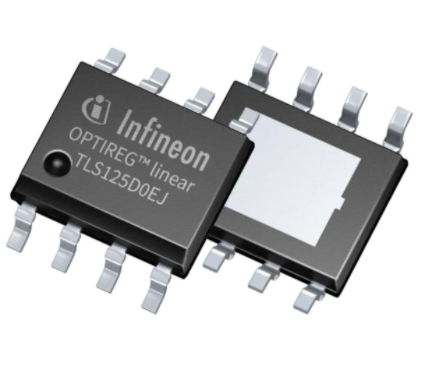
Step Down Voltage-Regulator with Reset
TLE 6365
Datasheet
1
Overview
1.1 Features
•
•
•
•
•
•
•
•
•
•
Step down converter
Supply Over- and Under-Voltage-Lockout
Low Output voltage tolerance
Output Overvoltage Lockout
Output Under-Voltage-Reset with delay
Overtemperature Shutdown
Wide Ambient operation range -40°C to 125°C
Wide Supply voltage operation range
Very low current consumption
Very small P-DSO-8 SMD package
P-DSO-8-3
Type
Ordering Code
Package
TLE 6365 G
Q67006-A9515
P-DSO-8-3
Functional description
General
The TLE 6365 G is a power supply circuit especially designed for automotive
applications.
The device is based on Infineon’s power technology SPT® which allows bipolar and
CMOS control circuitry to be integrated with DMOS power devices on the same
monolithic circuitry.
The TLE 6365 G contains a buck converter and a power on reset feature to start up the
system.
The very small P-DSO-8-3 SMD package meets the application requierements.
It delivers a precise 5V fully short circuit protected output voltage.
Furthermore, the build-in features like under- and overvoltage lockout for supply- and
output-voltage and the overtemperature shutdown feature increase the reliability of the
TLE 6365 G supply system.
Data Sheet Rev. 1.7
1
2003-06-02
�TLE 6365
1.2
Pin Definitions and Functions
Pin
No
Symbol Function
1
R
Reference Input; an external resistor from this pin to GND
determines the reference current and so the oscillator / switching
frequency
2
RO
Reset Output; open drain output from reset comparator with an
internal pull up resistor
3
BUC
Buck-Converter Compensation Input; output of internal error
amplifier; for loop-compensation and therefore stability connect
an external R-C-series combination to GND.
4
GND
Ground; analog signal ground
5
VCC
Output Voltage Input; feedback input (with integrated resistor
devider) and logic supply input; external blocking capacitor
necessary
7
BUO
Buck Converter Output; source of the integrated power-DMOS
6
BDS
Buck Driver Supply Input; voltage to drive the buck converter
powerstage
8
VS
Supply Voltage Input; buck converter input voltage; external
blocking capacitor necessary.
Pin Configuration
R
1
8
VS
RO
2
7
BUO
BUC
3
6
BDS
GND
4
5
VCC
P-DSO-8-3
Figure 1
Pin Configuration (top view)
Data Sheet Rev. 1.7
2
2003-06-02
�TLE 6365
1.3
Block Diagram
VS
8
Biasing and VREF
BUC
6
Buck
Converter
3
7
TLE 6365 G
R
1
Reference
Current
Generator
and
Oscillator
Undervoltage
Reset
Generator
4
Figure 2
Vinternal
5
2
BDS
BUO
VCC
RO
GND
Block Diagram
Data Sheet Rev. 1.7
3
2003-06-02
�TLE 6365
1.4
Absolute Maximum Ratings
Parameter
Symbol
Limit Values
min.
max.
Unit
Remarks
Voltages
Supply voltage
VS
– 0.3
46
V
Buck output voltage
VBUO
–1
46
V
Buck driver supply voltage
VBDS
– 0.3
55
V
Buck compensation input
voltage
VBUC
– 0.3
6.8
V
Logic supply voltage
VCC
– 0.3
6.8
V
Reset output voltage
VRO
– 0.3
6.8
V
Current reference voltage
VR
– 0.3
6.8
V
ESD-Protection (Human Body Model; R=1,5kΩ; C=100pF)
all pins to GND
VHBM
–2
2
kV
Tj
Tstg
– 40
150
°C
–
– 50
150
°C
–
Temperatures
Junction temperature
Storage temperature
Note: Stresses above those listed here may cause permanent damage to the device.
Exposure to absolute maximum rating conditions for extended periods may affect
device reliability.
Data Sheet Rev. 1.7
4
2003-06-02
�TLE 6365
1.5
Operating Range
Parameter
Symbol
Limit Values
min.
max.
Unit
Remarks
Supply voltage
VS
– 0.3
40
V
Supply voltage
VS
5
35
V
VS increasing
Supply voltage
VS
4.5
36
V
VS decreasing
Supply voltage
VS
– 0.3
4.5
V
Buck-Converter
OFF
Buck output voltage
VBUO
– 0.6
40
V
Buck driver supply voltage
VBDS
– 0.3
50
V
Buck compensation input
voltage
VBUC
0
3.0
V
Logic supply voltage
VCC
4.0
6.2
V
Reset output voltage
VRO
– 0.3
VCC
+0.3
V
Current reference voltage
VCREF
0
1.23
V
Junction temperature
Tj
– 40
150
°C
180
K/W
Thermal Resistance
Junction ambient
Data Sheet Rev. 1.7
Rthj-a
5
–
2003-06-02
�TLE 6365
1.6
Electrical Characteristics
8V< VS < 35V; 4.75V< VCC
很抱歉,暂时无法提供与“TLE6365”相匹配的价格&库存,您可以联系我们找货
免费人工找货