Data Sheet TLE 7230R
Smart Octal Low-Side Switch
Features
Product Summary
♦ Protection
Supply voltage
VS
4.5 – 5.5 V
Overload, short circuit
Drain source clamping voltage VDS(AZ)max 60
V
Overtemperature
Overvoltage
On resistance
RON
0.8
Ω
♦ Low Quiescent Current< 10µA
♦ 16 bit SPI (for Daisychain)
♦ Direct Parallel Control of Four Channels
♦ PWM input (demux)
♦ Parallel Inputs High or Low Active Programmable
♦ Programmable functions
Boolean operation
Overload behavior
Overtemperature behavior
Switching time
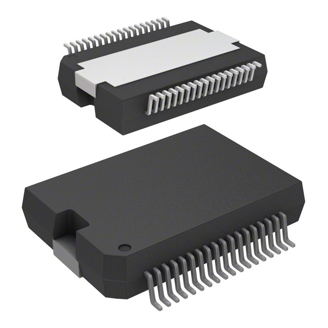
Power PG-DSO 36-47
♦ General Fault Flag
♦ Digital Ports Compatible to 5V and 3,3 V Micro Controllers
♦ Electrostatic Discharge (ESD) Protection
♦ Full reverse current capability without latch up
♦ Green Product (RoHS compliant)
♦ AEC qualified
Application
• µC-compatible 8-channel low-side switch
• Switch for Automotive and Industrial Applications
• Solenoids, Relays and Resistive Loads
General description
The TLE 7230 R is an Octal Low-Side Switch in Smart Power Technology (SPT) with a Serial Peripheral Interface (SPI) and eight open drain DMOS output stages. It is protected by embedded protection
functions and designed for automotive and industrial applications. The output stages are controlled
via an SPI Interface. Additionally, four channels can be controlled in parallel for PWM applications.
These features make the TLE 7230 R particularly suitable for engine management and body systems.
Detailed Block Diagram
PRG
GND
RESET
FAULT
VS
VDO
VS
VBB
Protection
Functions
IN1
IN2
as Ch. 1
IN3
as Ch. 1
LOGIC
Output Stage
IN4
as Ch. 1
16
SCLK
SI
CS
OUT1
8
Serial Interface
SPI
4
1
Output Control
Buffer
8
OUT8
SO
V3.4
GND
Page
1
2009-07-15
�Data Sheet TLE 7230R
Power SO 36 package
Pin Description
Pin
1
2
3
4
5
6
7
8
9
10
11
12
13
14
15
16
17
18
19
20
21
22
23
24
25
Symbol
GND
NC
NC
OUT1
OUT2
IN1
IN2
VS
Reset
CS
PRG
IN3
IN4
OUT3
OUT4
NC
NC
GND
GND
NC
NC
OUT5
OUT6
NC
VDO
26
27
28
29
30
31
32
33
34
35
36
Fault
SO
SCLK
SI
NC
NC
OUT7
OUT8
NC
NC
GND
Pin Configuration (Top view)
Function
Ground
not connected
not connected
Output Channel 1
Output Channel 2
Input Channel 1
Input Channel 2
Supply Voltage
Reset
Chip Select
Program
Input Channel 3
Input Channel 4
Output Channel 3
Output Channel 4
not connected
not connected
Ground
Ground
not connected
not connected
Output Channel 5
Output Channel 6
not connected
Supply for digital
Outputs
General Fault Flag
Serial Data Output
Serial Clock
Serial Data Input
not connected
not connected
Output Channel 7
Output Channel 8
not connected
not connected
Ground
1
2
3
4
5
6
7
8
9
10
11
12
13
14
15
16
17
18
GND
NC
NC
Out1
Out2
IN1
IN2
VS
Reset
CS
PRG
IN3
IN4
Out3
Out4
NC
NC
GND
GND
NC
NC
Out8
Out7
NC
NC
SI
SCLK
SO
Fault
VDO
NC
Out6
Out5
NC
NC
GND
36
35
34
33
32
31
30
29
28
27
26
25
24
23
22
21
20
19
Power- PG-DSO-36
Heat Slug internally connected to ground pins
V3.4
Page
2
2009-07-15
�Data Sheet TLE 7230R
Maximum Ratings for Tj = – 40°C to 150°C
Parameter
Supply Voltage
Continuous Drain Source Voltage (OUT1...OUT8)
Symbol
VS, V VDO
VDS
Values
-0.3 ... + 6
48
Unit
V
V
Input Voltage, All Inputs and Data Lines
Operating Temperature Range
Storage Temperature Range
Output Current per Channel (see el. characteristics)
VIN
Tj
Tstg
ID(lim)
- 0.3 ... + 6
- 40 ... + 150
- 55 ... + 150
ID(lim)min
V
°C
Reverse current per channel
IR
- ID(lim)min
A
A
Output Clamping Energy per channel
(single pulse, triangular shape, individual switch off)
ID = 0.3 A, TJ(start) = 150°C
ID = 0.4 A, TJ(start) = 85°C
Output Clamping Energy per channel
(repetitive pulses, triangular shape)
ID = 0.25 A, TJ(aver.) = 150°C, repetitive (1⋅ 106 cycles)
EAS
Maximum Battery Voltage for full
OVL = 0
4
short circuit protection (single pulse)
OVL = 1
Electrostatic Discharge Voltage (Human Body Model)
HBM according to EIA/JESD 22-A114
Output 1-8 Pins
All other Pins
VBAT(SC)
20
28
V
VESD
VESD
2000
2000
V
V
mJ
50
65
EAR
mJ
15
DIN Humidity Category, DIN 40 040
IEC Climatic Category, DIN IEC 68-1
E
40/150/56
Thermal Characteristics
Parameter
Symbol
Thermal Resistance, Junction – Case
(all channels active, 0.3W power dissipation each channel)
(only one channel active, 0.5W power dissipation)
RthJC
V3.4
Page
3
Values
min
max
---
2.6
12
Unit
K/W
2009-07-15
�Data Sheet TLE 7230R
Electrical Characteristics
Parameter and Conditions
VS = 4.5 to 5.5 V ; VVDO = 3.0 to 5.5V;
Tj = - 40 °C to + 150 °C ; Reset = H
(unless otherwise specified)
Symbol
Values
min
Unit
typ
max
--
5.5
V
5.5
V
1. Power Supply, Reset
Supply Voltage1
VS
4.5
Supply Voltage Digital Output
VVDO
3.0
Supply Current
Supply Current (reset mode)
IS
IS(reset)
---
3
5
10
mA
µA
tReset,min
10
--
--
µs
TJ = 25°C 2
TJ = 150°C
RDS(ON)
---
0.8
--
1
1.7
Ω
Output OFF
VDS(AZ)
48
--
60
V
ID(lim)
1
2
A
ID(lkg)
--
2
µA
tON
--
15
60
µs
tOFF
--
15
60
µs
3. Digital Inputs
Input Low Voltage
Input High Voltage
Input Voltage Hysteresis
VINL
VINH
VINHys
- 0.3
2.0
--100
1.0
--
V
V
mV
Input Pull Down/Up Current (IN1 ... IN4)
PRG, Reset Pull Up Current
Input Pull Down Current (SI, SCLK)
IIN(1..4)
IIN(PRG,Res)
IIN(SI,SCLK)
20
20
10
50
50
20
100
100
50
µA
µA
µA
Input Pull Up Current (CS)
IIN(CS)
10
20
50
µA
Reset = L
Minimum Reset Duration
2. Power Outputs
ON Resistance VS = 5 V; ID = 500 mA
Output Clamping Voltage
Current Limit
Output Leakage Current
VReset = L
Tj =125°C ; Vbb=13.5V
Turn-On Time
SLE = 0
ID = 0.5 A, resistive load
SLE = 1
Turn-Off Time
SLE = 0
ID = 0.5 A, resistive load
SLE = 1
4. Digital Outputs (SO, Fault)
SO High State Output Voltage
SO Low State Output Voltage
ISOH = 2 mA
VVDO = 5V
VVDO = 3V
ISOL = 2.5 mA
VSOH
V
VVDO–0.4 --
--
VVDO–0.6
Output Tristate Leakage Current, CS = H, 0 ≤ VSO ≤ VS
Fault Output Low Voltage
IFAULT = 1.6 mA
1
--
VSOL
--
--
0.4
V
ISOlkg
VFAULTL
-10
--
0
--
10
0.4
µA
V
For VS < 4.5V the power stages are switched according the input signals and data bits or are definitely switched
off. The undervoltage reset becomes active at VS = 3V (typ. value) and is specified by design. Not subject to
production test.
V3.4
Page
4
2009-07-15
�Data Sheet TLE 7230R
Electrical Characteristics cont.
Parameter and Conditions
VS = 4.5 to 5.5 V; VVDO = 3.0 to 5.5V;
Tj = - 40 °C to + 150 °C ; Reset = H
(unless otherwise specified)
Symbol
Values
min
Unit
typ
max
5. Diagnostic Functions
Open Load Detection Voltage
VDS(OL)
VS -2.5 VS -2
Output Pull Down Current
IPD(OL)
50
Fault Delay Time
Overload switch off delay time
td(fault)
Td(off)
50
10
Short to Ground Detection Voltage
Short to Ground Detection Current
VDS(SHG)
ISHG
VS -3.6 VS -3.0 VS -2.6 V
-50
-100
-150
µA
Overload Threshold Current
Overtemperature Shutdown Threshold2,4
Hysteresis2
ID(OVL) 1...8
Tth(sd)
Thys
1
170
--
6. SPI-Timing (for VVDO = 4.5V to 5.5V)
Serial Clock Frequency (depending on SO load)
Serial Clock Period (1/fclk)
fSCK
VS -1.3
V
90
150
µA
100
200
50
µs
µs
-10
2
200
--
A
°C
K
tp(SCK)
DC
200
---
5
--
MHz
ns
tSCKH
tSCKL
tlead
50
50
250
----
----
ns
ns
ns
Enable Lag Time (falling edge of CLK to rising edge ofCS) tlag
250
---
--
ns
Data Setup Time (required time SI to falling of CLK)
Data Hold Time (falling edge of CLK to SI)
Disable Time2
tSU
tH
tDIS
20
20
--
----
--150
ns
ns
ns
Transfer Delay Time3
(CS high time between two accesses)
Data Valid Time (for VVDO = 4.5V to 5.5V)
tdt
200
--
--
ns
tvalid
----
100
120
150
ns
tvalid
----
100
140
240
ns
Serial Clock High Time
Serial Clock Low Time
Enable Lead Time (falling edge of CS to rising edge of
CLK)
Data Valid Time (for VVDO = 3.0V to 3.6V)
2
3
CL = 50 pF2
CL = 100 pF2
CL = 220 pF2
CL = 50 pF2
CL = 100 pF2
CL = 220 pF2
This parameter is not subject to production test. Specified by design.
This time is necessary between two write accesses. To get the correct diagnostic information, the transfer delay
time has to be extended to the maximum fault delay time td(fault)max = 200µs.
V3.4
Page
5
2009-07-15
�Data Sheet TLE 7230R
Functional Description
The TLE 7230 R is an octal low-side power switch with a serial peripheral interface (SPI) for control
and diagnostic feedback of the 8 power DMOS switches. The power transistors are protected4 against
overload (current limitation), overtemperature and overvoltage (by active zener clamping). The diagnostic logic recognizes a fault condition which can be read out via the serial diagnostic output (SO).
Output Stage Control: Parallel Control or SPI Control
The Output stages can be controlled by parallel Inputs or by SPI commands. The IC can be programmed via SPI to switch the outputs according to the corresponding SPI command bit or to a combination of SPI bit and parallel input signal. The Boolean logic combination of parallel and serial signal
is programmable by SPI to logic "AND" or "OR". The respective SPI data bits are active high and the
parallel Inputs are active high or low according to the PRG pin (see pin description).
Boolean operation:
The logic combination of the parallel and the
serial input signal can be configured by an
SPI command for each of the 8 channels
individually. Logic "AND" or logic "OR" is
possible.
parallel in
off
off
on
on
serial in
off
on
off
on
Output "OR"
off
on
on
on
Output "AND"
off
off
off
on
Map able parallel input (IN 4):
The parallel input 4 (IN4) can be defined via SPI command as parallel input for one or more power
outputs. Depending on the Input Map Register this input can be used to control one up to eight of the
parallel outputs. Default operation: IN4 is the parallel input for channel 4.
Input Map register
Input buffer
IN n (1..3)
Input buffer
IN 4
Boolean register
Input buffer
IN 4
Boolean register
&
&
Output Latch
≥1
Output Latch
≥1
serial controll register
Channel 4 to 8
serial controll register
Channel 1 to 3
Signal logic channel 1 to 3
Input Map register
Signal logic channel 4 to 8
Switching speed / Slew rate:
The switching speed / slew rate of each individual channel can be configured by SPI for slow or fast
switching speed (max. 15µs or 60µs).
Overtemperature Behavior:
Each channel has an overtemperature sensor and is individually protected against overtemperature.
As soon as an overtemperature event occurs, the channel is immediately turned off and the overtemperature information is reported by diagnosis. In this case, there are two different behaviors of the
affected channel that can be selected by SPI (for all channels individually).
• Auto restart: as long as the input signal of the channel remains on (e.g. parallel input high) the
channel turns automatically on again after cooling down.
• Latching: In the event of an overtemperature shutdown, the channel stays off until the overtemperature latch is reset by a new LàH transition of the input signal.
4
The integrated protection functions help to prevent damage to the device under fault conditions and may not be
used in normal operation or permanently.
V3.4
Page
6
2009-07-15
�Data Sheet TLE 7230R
Note: The overtemperature sensors of the output channels are only active if the channel is turned on.
Low Quiescent Current Mode (Sleep Mode) :
By applying a low signal at the Reset Pin, the device can be set to sleep mode. In this mode, all outputs are turned off, diagnosis and biasing are disabled, the diagnosis and the on/off register are reset
and the current consumption is drastically reduced (V3.3
V3.3 ->
V3.2
V3.1 ->
V3.2
V3.4
Date
2009-07-15
2008-07-22
Changes
Short to Ground Detection Voltage min limit changed from VS -3.4 to VS
-3.6
Version Change : changed Package naming only
2007-06-11
Version Change
2007-06-11
Revision History cleaned – only “final” data sheet related contents
Page
14
2009-07-15
�Data Sheet TLE 7230R
Edition 2009-07-1415
Published by
Infineon Technologies AG
81726 Munich, Germany
© 2009 Infineon Technologies AG
All Rights Reserved.
Legal Disclaimer
The information given in this document shall in no event be regarded as a guarantee of conditions or characteristics. With respect to any examples or hints given herein, any typical values stated herein and/or any information
regarding the application of the device, Infineon Technologies hereby disclaims any and all warranties and liabilities of any kind, including without limitation, warranties of non-infringement of intellectual property rights of any
third party.
Information
For further information on technology, delivery terms and conditions and prices, please contact the nearest Infineon Technologies Office (www.infineon.com).
Warnings
Due to technical requirements, components may contain dangerous substances. For information on the types in
question, please contact the nearest Infineon Technologies Office.
Infineon Technologies components may be used in life-support devices or systems only with the express written
approval of Infineon Technologies, if a failure of such components can reasonably be expected to cause the
failure of that life-support device or system or to affect the safety or effectiveness of that device or system. Life
support devices or systems are intended to be implanted in the human body or to support and/or maintain and
sustain and/or protect human life. If they fail, it is reasonable to assume that the health of the user or other persons may be endangered.
V3.4
Page
15
2009-07-15
�


 工商网监
湘ICP备2023018690号
工商网监
湘ICP备2023018690号
