Dual Low Drop Voltage Regulator
TLE 7469
Features
•
•
•
•
•
•
•
•
•
•
•
•
•
•
•
Dual output
5 V (±2%), 215mA and 2.6 V1) (±4%), 200mA or
5 V (±2%), 215mA and 3.3 V (±3%), 200mA
Ultra low quiescent current consumption < 55 µA
Inhibit function
Very low dropout voltage
Reset with power-on delay
Early Warning comparator
Window watchdog
Power sequencing for dual voltage µC
Output protected against short circuit
Wide operation range: up to 45 V
Wide temperature range: -40 °C to 150 °C
Overtemperature protection
Overload protection
Green Product (RoHS compliant)
AEC Qualified
Functional Description
The TLE 7469 is a monolithic integrated voltage regulator with two voltage outputs
specially designed to supply microcontrollers with dual supply voltage: 2.6 V1) or 3.3 V
core and 5 V I/O voltage like the Infineon XC164 and XC161.
1) 2.5 V nominal specification range of most µCs is compatible with the 2.6 V output voltage range of the
TLE 7469.
Type
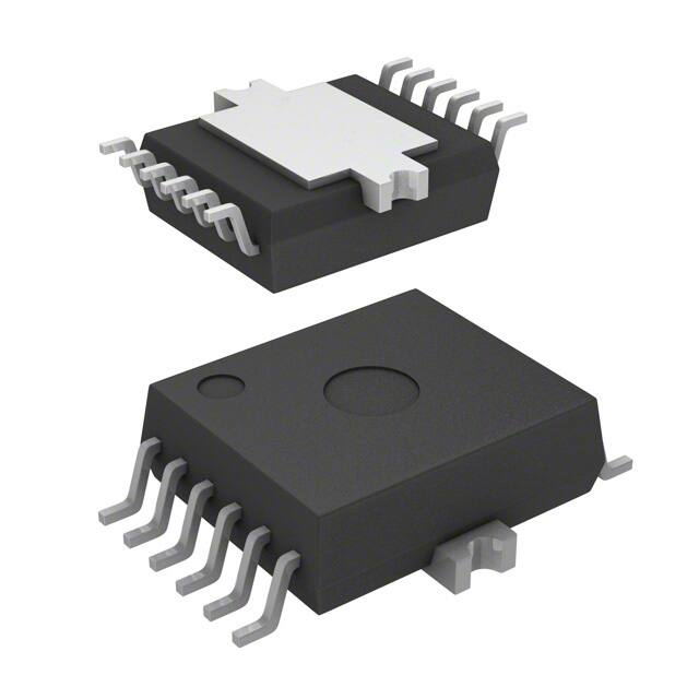
Package
TLE 7469 GV52
PG-DSO-12
TLE 7469 GV53
PG-DSO-12
Data Sheet
1
Rev. 1.6, 2008-01-22
�TLE 7469
The voltage regulator features an integrated reset circuitry which monitors the 2.6 V/
3.3 V supply voltage. At power on the reset checks both supply voltages and performs
the power-on reset with an adjustable delay time. The voltage difference is kept in the
range -0.5 V < (VQ1 - VQ2) < 3.0 V even during power-on and power-down time enabling
save µC operation without external clamping. Using the integrated early warning
comparator an external voltage can be supervised. An integrated output sink current
circuitry keeps the voltage at the Q1 pin below 5.5 V even when reverse currents are
applied. Thus connected devices are protected from overvoltage damage. The regulator
can be shut down via the Inhibit input causing the current consumption to drop below
9 µA.
The TLE 7469 is designed for use under the severe conditions of automotive
applications, and is therefore equipped with protection functions against overload, short
circuit and overtemperature. It operates in the wide junction temperature range from
-40 °C to 150 °C and offers the low quiescent current consumption required for body
applications.
For applications requiring extremely low noise levels the Infineon voltage regulator family
TLE 42XY and TLE 44XY is more suited than the TLE 7469. A mV-range output noise
on the TLE 7469 caused by the charge pump operation is unavoidable due to the ultra
low quiescent current concept.
Data Sheet
2
Rev. 1.6, 2008-01-22
�TLE 7469
I2
TLE 7469
12
10
Q2
Q1
Overtemperature
Shutdown
Bandgap
Reference
Reset
Generator
and
Window
Watchdog
1
Charge
Pump
SI
INH
I1
5
7
8
2
9
Early
Warning
4
RO
WDI
DT
SO
Inhibit
1
3
Q1
Overtemperature
Shutdown
1
Charge
Pump
GND
11
Figure 1
Data Sheet
AEB03530_1.VSD
Block Diagram
3
Rev. 1.6, 2008-01-22
�TLE 7469
t
PG-DSO-12
I1
1
12
I2
INH
2
11
GND
Q1
3
10
Q2
SO
4
9
RO
WDI
5
8
SI
GND
6
7
DT
AEP03531.VSD
Figure 2
Pin Configuration (top view)
Table 1
Pin Definitions and Functions
Pin No. Symb. Function
1
I1
Input voltage 1; block to ground directly at the IC with a 100 nF
ceramic capacitor
2
INH
Inhibit Input; low level disables the IC. Integrated pull-down resistor
3
Q1
Output voltage 1; 5.0 V, block to GND with a capacitor
CQ1 ≥ 1 µF, ESR < 6 Ω at 10 kHz
4
SO
Sense output; Output of Early Warning Comparator, open collector
output
5
WDI
Watchdog Input; Trigger Input for Watchdog pulses
6, 11
GND
Ground; Pin 6, 11 and heat slug must be connected to GND
7
DT
DT Delay timing; connect to GND, Q1 or Q2 to select Reset and
Watchdog timing
8
SI
Sense input; Input for Early Warning comparator
9
RO
Reset output; open collector output with integrated 20 kΩ pull-up
resistor
10
Q2
Output voltage 2; 2.6 V (TLE 7469 GV52), 3.3 V (TLE 7469 GV53);
block to GND with a capacitor CQ2 ≥ 1 µF, ESR < 6 Ω at 10 kHz
12
I2
Input voltage 2; block to ground directly at the IC with a 100 nF
ceramic capacitor
Data Sheet
4
Rev. 1.6, 2008-01-22
�TLE 7469
Table 2
Absolute Maximum Ratings
-40 °C < Tj < 150 °C
Parameter
Symbol
Limit Values
Unit
Remarks
Min.
Max.
VI1
II1
-0.3
45
V
–
–
–
mA
Internally limited
VI2
II2
-0.3
45
V
–
–
–
mA
Internally limited
VQ1
VQ1
IQ1
-0.3
5.5
V
Permanent
-0.3
6.2
V
t < 10 s1)
–
2
mA
Internally limited
VQ2
VQ2
IQ2
-0.3
5.5
V
Permanent
-0.3
6.2
V
t < 10 s1)
–
–
mA
Internally limited
VINH
-0.3
45
V
Observe current limit
IINH
-1
1
mA
–
VRO
VRO
IRO
-0.3
5.5
V
Permanent
-0.3
6.2
V
t < 10 s1)
–
–
mA
internally limited
VDT
VDT
IDT
-0.3
5.5
V
Permanent
-0.3
6.2
V
t < 10 s1)
-5
5
mA
–
Input I1
Voltage
Current
Input I2
Voltage
Current
Output Q1
Voltage
Voltage
Current
Output Q2
Voltage
Voltage
Current
Inhibit Input INH
Voltage
Current
IINHmax2)
Reset Output RO
Voltage
Voltage
Current
Delay Timing DT
Voltage
Voltage
Current
Data Sheet
5
Rev. 1.6, 2008-01-22
�TLE 7469
Table 2
Absolute Maximum Ratings (cont’d)
-40 °C < Tj < 150 °C
Parameter
Symbol
Limit Values
Unit
Remarks
Min.
Max.
VWDI
VWDI
IWDI
-0.3
5.5
V
Permanent
-0.3
6.2
V
t < 10 s1)
–
–
mA
internally limited
VSI
-0.3
45
V
Observe current limit
ISI
-1
1
mA
–
VSO
VSO
ISO
-0.3
5.5
V
Permanent
-0.3
6.2
V
t < 10 s1)
–
–
mA
internally limited
Tj
Tstg
–
150
°C
–
-50
150
°C
–
Watchdog Input WDI
Voltage
Voltage
Current
Sense Input SI
Voltage
Current
ISImax2)
Sense Output SO
Voltage
Voltage
Current
Temperatures
Junction temperature
Storage temperature
1) Exposure to these absolute maximum ratings for extended periods (t > 10 s) may affect device reliability.
2) External resistor required to keep current below absolute maximum rating when voltages ≥ 5.5 V are applied.
Note: Maximum ratings are absolute ratings; exceeding any one of these values may
cause irreversible damage to the integrated circuit. Integrated protection functions
are designed to prevent IC destruction under fault conditions. Fault conditions are
considered as outside normal operating range. Protections functions are not
designed for continuous repetitive operation.
Data Sheet
6
Rev. 1.6, 2008-01-22
�TLE 7469
Table 3
Operating Range
Parameter
Symbol
Limit Values
Unit
Remarks
Min.
Max.
5.6
45
V
–
6.0
45
V
4.2
45
V
VI1 > 8V
VI1 < 8V
-40
150
°C
–
–
4.4
K/W
–
–
107
K/W
PCB, only Footprint1)
Junction ambient
Rthjc
Rthj-a
Rthj-a
–
58
K/W
PCB Heat Sink Area
300 mm2 1)
Junction ambient
Rthj-a
–
48
K/W
PCB Heat Sink Area
600 mm2 1)
Input voltage
Input voltage
Input voltage
Junction temperature
VI1
VI2
VI2
Tj
Thermal Resistances PG-DSO-12
Junction case
Junction ambient
1) Package mounted on PCB 80 × 80 × 1.5 mm3; 35µ Cu; 5µ Sn; zero airflow; 85 °C ambient temperature.
Note: In the operating range the functions given in the circuit description are fulfilled.
Data Sheet
7
Rev. 1.6, 2008-01-22
�TLE 7469
Table 4
Electrical Characteristics
VI1 = 13.5 V; VI2 = 13.5 V; -40 °C < Tj < 150 °C; unless otherwise specified
Parameter
Symbol
Limit Values
Min.
Typ.
Max.
Unit
Test Condition
Output Q1
Output voltage
VQ1
4.90
5.0
5.10
V
1 mA < IQ1 < 215 mA,
6 V < VI1 < 16 V
Output current
limitation
IQ1
320
–
700
mA
VQ1 = 4.0 V
–
300
600
mV
IQ1 = 215 mA1)
Output drop voltage; VDRQ1
VDRQ1 = VI1 - VQ1
Load regulation
∆VQ1,Lo
–
25
60
mV
1 mA < IQ1 < 215 mA
Line regulation
∆VQ1,Li
–
20
50
mV
Power Supply Ripple PSRR
Rejection
–
60
–
dB
VQ,REV
–
–
5.5
V
IQ1 = 1 mA,
10 V < VI < 28 V
fr = 100 Hz,
Vr = 1 Vpp
IQ,REV = 1 mA,
VINH = 0 V
Output voltage
VQ2
2.50
2.60
2.70
V
1 mA < IQ2 < 200 mA,
6 V < VI2 < 16 V,
TLE 7469 GV52
Output voltage
VQ2
3.20
3.30
3.40
V
1 mA < IQ2 < 200 mA,
6 V < VI2 < 16 V,
TLE 7469 GV53
Absolute differential
voltage
VQ1 - VQ2 -0.5
–
3.0
V
VQ1, VQ2 > 1 V
Output current
limitation
IQ2
300
–
550
mA
VQ2 = 2.0 V
Load regulation
∆VQ2,Lo
–
25
60
mV
1 mA < IQ2 < 200 mA
Line regulation
∆VQ22,Li
–
20
50
mV
–
60
–
dB
IQ2 = 1 mA,
10 V < VI < 28 V
fr = 100 Hz,
Vr = 1 Vpp
Reverse Output
Current Protection
Output Q2
Power Supply Ripple PSRR
Rejection
Data Sheet
8
Rev. 1.6, 2008-01-22
�TLE 7469
Table 4
Electrical Characteristics (cont’d)
VI1 = 13.5 V; VI2 = 13.5 V; -40 °C < Tj < 150 °C; unless otherwise specified
Parameter
Symbol
Limit Values
Unit
Test Condition
IQ2 = IQ1 = 100 µA,
Tj < 80 °C
VINH = 0 V,
Tj < 80 °C
Min.
Typ.
Max.
Quiescent current;
Iq
Iq = II1 + II2 - IQ1 - IQ2
–
–
55
µA
Iq
–
5
9
µA
VINH ON
VINH OFF
IINH ON
IINH OFF
–
–
3.1
V
0.8
–
–
V
–
3
4
µA
–
0.5
1
µA
VQ1 & VQ2 on
VQ1 & VQ2 off
VINH = 5 V
VINH = 0 V, Tj < 80 °C
Threshold Fast
Timing Select
VDT,FAST
4.5
–
–
V
–
Threshold Slow
Timing Select
VDT,SLOW 2.3
–
3.3
V
TLE 7469 GV52
Threshold Slow
Timing Select
VDT,SLOW 2.3
–
3.6
V
TLE 7469 GV53
–
–
0.8
V
–
Current Consumption
Quiescent current;
inhibited
Inhibit Input INH
Turn-on Voltage
Turn-off Voltage
H-input current
L-input current
Delay Timing DT
Threshold Watchdog VDT,OFF
Turn Off2)
Watchdog Input WDI
H-input voltage
threshold
VWDIH
–
–
3.0
V
–
L-input voltage
threshold
VWDIL
–
–
0.8
V
–
Watchdog sampling
time
tsam
0.20
0.25
0.30
ms
Fast Timing
0.80
1.00
1.20
ms
Slow Timing
Ignore window time
tOW
25.6
32.0
38.4
ms
Fast Timing
102
128
154
ms
Slow Timing
25.6
32.0
38.4
ms
Fast Timing
102
128
154
ms
Slow Timing
Open window time
Data Sheet
tOW
9
Rev. 1.6, 2008-01-22
�TLE 7469
Table 4
Electrical Characteristics (cont’d)
VI1 = 13.5 V; VI2 = 13.5 V; -40 °C < Tj < 150 °C; unless otherwise specified
Parameter
Closed window time
Window watchdog
trigger time
Symbol
tCW
tWD
Limit Values
Unit
Test Condition
Min.
Typ.
Max.
25.6
32.0
38.4
ms
Fast Timing
102
128
154
ms
Slow Timing
39.0
44.8
50.6
ms
Fast Timing
156
179
202
ms
Slow Timing
2.48
V
TLE 7469 GV52,
VQ2 decreasing
mV
TLE 7469 GV52
V
TLE 7469 GV53,
VQ2 decreasing
mV
TLE 7469 GV53
Reset Output RO
Reset switching
threshold 2
VRT2
2.35
2.38
Reset Headroom 2
VRH2
VRT2
130
190
3.00
3.07
VRH2
VRH2
165
240
–
45
–
mV
TLE 7469 GV52 3)
–
60
–
mV
TLE 7469 GV53 4)
Reset switching
threshold 2
Reset Headroom 2
Reset hysteresis 2
3.15
Reset switching
threshold 1
VRT1
4.50
4.65
4.80
V
VQ1 decreasing
Reset hysteresis 1
VRH1
IRO
VROL
–
90
–
mV
–
–
–
1
mA
–
0.15
0.25
V
VQ = 5 V, VRO = 0.5 V
VQ2 ≥ 1 V
4.5
–
–
V
–
10
20
40
kΩ
Internally connected to
Q1
6.0
8.0
10.0
ms
Fast Timing
(VDT ≥ 4.5 V)
24.0
32.0
40
ms
Slow Timing
(VDT ≤ 3.3 V)
–
10
26
µs
–
Reset sink current
Reset output low
voltage
VROH
Integrated reset pull- RRO
Reset high voltage
up resistor
Power-up Reset
delay time
TRD
Reset Reaction Time TRR
Data Sheet
10
Rev. 1.6, 2008-01-22
�TLE 7469
Table 4
Electrical Characteristics (cont’d)
VI1 = 13.5 V; VI2 = 13.5 V; -40 °C < Tj < 150 °C; unless otherwise specified
Parameter
Symbol
Limit Values
Min.
Typ.
Max.
1.10
1.16
1.22
Unit
Test Condition
V
VSI increasing (see
Input Voltage Sense
Sense threshold high VSIH
Figure 4)
Sense threshold low VSIL
1.06
1.12
1.18
V
VSI decreasing (see
Figure 4)
Sense output low
voltage
VSOL
–
0.1
0.4
V
External SO pull-up
resistor
RSO ext
9.2
–
–
kΩ
VSI < 1.01 V;
VI1 > 4.20 V;
ISO = 0.5 mA
VQ1 = 5V
Sense input current
ISI
tpd SO LH
-1
0.1
1
µA
VSI = 5 V
–
4.0
–
µs
–
tpd SO HL
–
4.0
–
µs
–
Sense high reaction
time
Sense low reaction
time
1) Measured when the output voltage has dropped 100 mV from the nominal Value obtained at VI1 = 13.5 V,
VI2 = 13.5 V.
2) Watchdog off, Reset in slow mode.
3) Specified by design, not subject of production test.
4) Specified by design, not subject of production test.
Data Sheet
11
Rev. 1.6, 2008-01-22
�TLE 7469
Application Information
R Vi *
VBat
TLE 7469
I2
47
µF
Q2
100 nF
100 k Ω
e. g.
Ignition
Key
DT
INH
47
µF
1 µF
WDI
RO
SI
XC 164
SO
10 kΩ
Q1
I1
100 nF
GND
1 µF
= Optional
Figure 3
47
µF
AEA03529_2.VSD
Application Diagram with Typical External Components
A typical application of the TLE 7469 is shown in Figure 3. To prevent the regulation
loop from oscillating a ceramic capacitor of CQ1/2 ≥ 1 µF is required at each of the outputs
Q1 and Q2. In contrast to most low drop voltage regulators the TLE 7469 only needs
moderate capacitance at the outputs and tolerates ceramic capacitors to keep the
stability. This offers more design flexibility to the circuit designer enabling the IC also to
operate without tantalum capacitors.
Additional a buffer capacitor CB of > 10µF should be used for each output Q1 and Q2 to
suppress influences from load surges to the voltage levels. This one can either be an
aluminum electrolytic capacitor or a tantalum capacitor following the application
requirements.
A general recommendation is to keep the drop over the equivalent serial resistor (ESR)
together with the discharge of the blocking capacitor below the Reset Headroom (e.g.
min. 130mV for the 2.6V Output).
Data Sheet
12
Rev. 1.6, 2008-01-22
�TLE 7469
Since the regulator output current roughly rises linearly with time the discharge of the
capacitor can be calculated as follows:
dVCB = dIQ*dt/CB
The drop across the ESR calculates as:
dVESR = dI*ESR
To prevent a reset the following relationship must be fullfilled:
dVC + dVESR < VRH2 = 130mV
Example: Assuming a load current step of dIQ = 50mA, a blocking capacitor of CQ =
22µF and a typical regulator reaction time under normal operating conditions of dt ~
25µs and for special dynamic load conditions, such as load step from very low base
load, a reaction time of dt ~ 75µs.
dVC = dIQ*dt/CB = 50mA * 25µs/22µF = 54mV
So for the ESR we can allow
dVESR = VRH2 - dVC = 130mV - 54mV = 76mV
The permissible ESR becomes:
ESR = dVESR / dIQ = 76mV/50mA = 1.52Ohm
During design-in of the TLE7469 product family, special care needs to be taken with
regards to the regulators reaction time to sudden load current changes starting from very
low pre-load as well as cyclic load changes. The application note “TLE7x Voltage
Regulators - Application Note about Transient Response at ultra low quiescent current
Voltage Regulators” (see 3_cip05405.pdf) gives important hints for successful design-in
of the Voltage Regulators of the TLE7x family.
As a dual regulator the TLE 7469 for correct operation should be always supplied at both
input pins I1 and I2 out of one voltage supply. The dual voltage regulator with both inputs
accessible, offers the possibility to reduce the power dissipation in the package. This can
be achived by two different input voltages or a Drop Resistor* RVi (see Figure 3) at the
input pin I2 for the 2.6V output. If one of this options is chosen,care should be taken, to
apply the device as descibed under “Table 3: Operating Range”.
The reset output RO features an integrated pull-up resistor. Thus it can be directly
coupled to the microcontroller reset input.
Data Sheet
13
Rev. 1.6, 2008-01-22
�TLE 7469
The sense comparator output SO is an open collector. An appropriate external pull-up
resistor is typ. 5.6 kΩ … 47 kΩ, the minimum value of 5.6 kΩ being defined by the max.
sink current capability of the SO output transistor. If the sense comparator is not used
the pull-up resistor can be spared. In this case the SI pin should be directly connected to
Q1 in order to keep the comparator inactive.
Sense
Input
Voltage
VSIH
VSIL
t
Sense
Output
t PD SO LH
t PD SO HL
High
Low
t
AED02559_7469
Figure 4
Data Sheet
Sense Timing Diagram
14
Rev. 1.6, 2008-01-22
�TLE 7469
Circuit Description
Power On Reset
In order to avoid any system failure, a sequence of several conditions has to be passed.
When the level of VQ2 reaches the reset threshold VRT, the signal at RO remains LOW
for the Power-up reset delay time TRD. Then a second comparator checks whether
VQ1 ≥ VRT1 and only if this test is passed the reset output is switched to HIGH. The Reset
output is only released (set to High level) if both output voltages have passed their
specific reset threshold VRT1/2. The reset function and timing is illustrated in Figure 5.
The reset reaction time TRR avoids wrong triggering caused by short “glitches” on the
VQ2-line. For power-fail, in case of VQ2 or VQ1 power down (VQ2 < VRT2 or VQ1 < VRT1 for
t > TRR) a logic LOW signal is generated at the pin RO to reset an external
microcontroller.
Data Sheet
15
Rev. 1.6, 2008-01-22
�TLE 7469
VI
t
VQ1
VRT1
t
VQ2
VRT2
TRR
VRO
TRD
t
TRR
TRD
TRD
VROH
VROL
t
AET03532.VSD
Figure 5
Reset Function and Timing Diagram
Watchdog Operation
The watchdog uses a fraction of the charge pump oscillator’s clock signal as timebase.
Connecting the DT pin to Q1 or to Q2 the watchdog timebase can be adjusted. The
watchdog can be turned off by a low level (VDT ≤ 0.8 V) applied to the DT pin. The timing
values used in this text refer to typ. values with DT connected to Q1 (fast timing).
Figure 6 shows the state diagram of the window watchdog (WWD). After power-on, the
reset output signal at the RO pin (microcontroller reset) is kept LOW for the reset delay
time TRD of typ. 8 ms. With the LOW to HIGH transition of the signal at RO the device
starts the ignore window time tCW (32 ms). During this window the signal at the WDI pin
is ignored. Next the WWD starts the open window. When a valid trigger signal is detected
during the open window a closed window is initialized immediately. A trigger signal within
Data Sheet
16
Rev. 1.6, 2008-01-22
�TLE 7469
the closed window is interpreted as a pretrigger failure and results in a reset. After the
closed window the open window with the duration tOW is started again. The open window
lasts at minimum until the trigger process has occurred, at maximum tOW is 32 ms (typ.
value with fast timing).
A HIGH to LOW transition of the watchdog trigger signal on pin WDI is taken as a trigger.
To avoid wrong triggering due to parasitic glitches two HIGH samples followed by two
LOW samples (sample period tsam typ. 0.25 ms) are decoded as a valid trigger (see
Figure 8). A reset is generated (RO goes LOW) if there is no trigger pulse during the
open window or if a pretrigger occurs during the closed window. The triggering is correct
also, if the first three samples (two HIGH one LOW) of the trigger pulse at pin WDI are
inside the closed window and only the fourth sample (the second LOW sample) is taken
in the open window.
Reset
Always
Trigger During
Closed Window
Ignore
Window
No Trigger During
Open Window
Always
Trigger
Closed
Window
Open
Window
No Trigger
AEA03533.VSD
Figure 6
Data Sheet
Window Watchdog State Diagram
17
Rev. 1.6, 2008-01-22
�TLE 7469
Vi/V
t
VQ/V
VRT
t
VRO/V
TRD
TRD
TRD
Normal operation
Power
Fail
trr
t rr
t
Wnd
Ingnore Wnd
Don’t care WDI
during IW
WDI/V
OW
CW
OW
CW
OW
CW
OW
t
(Wrong) Trigger
in CW
1. Correct Trigger
tWD,p
OW
No Trigger
in OW
t
Figure 7
Window Watchdog Signal Flow
Closed window
Open window
Watchdog
trigger signal
WDI
Valid
WDI
Not valid
t ECW
Data Sheet
Closed window
t EOW
= Watchdog decoder sample point
Figure 8
Open window
AET02952
Window Watchdog Definitions
18
Rev. 1.6, 2008-01-22
�TLE 7469
0.8
Index Marking
1
12x
0.4 +0.13
0.25 M C A B
5˚ ±3˚
35
Bottom View
7
6
6
0.25 B
12
1.6 ±0.1
(Metal)
4.2 ±0.1
(Metal)
(1.8 Mold)
6.4 ±0.11)
B
(Mold)
7
+0.075
0.25 -0
.0
10.3 ±0.3
7.6 +0.13
-0.1
12
B
0.7 ±0.15
7.8 ±0.1
(Heatslug)
(4.4 Mold)
0.1
7.5 ±0.11)
(1.55)
0+0.1
STANDOFF
2.35 ±0.1
(Body)
2.6 MAX.
Package Outlines
1
Heatslug
1
5x 1 = 5
5.1±0.1
(Metal)
1) Does not include plastic or metal protrusion of 0.15 max. per side
GPS09628
Figure 9
PG-DSO-12 (Plastic Green Dual Small Outline)
Green Product (RoHS compliant)
To meet the world-wide customer requirements for environmentally friendly products
and to be compliant with government regulations the device is available as a green
product. Green products are RoHS-Compliant (i.e Pb-free finish on leads and suitable
for Pb-free soldering according to IPC/JEDEC J-STD-020).
For further packge information, please visit our website:
http://www.infineon.com/packages.
Data Sheet
19
Dimensions in mm
Rev. 1.6, 2008-01-22
�TLE 7469
Revision History
Version
Date
Rev. 1.6
2008-01-22 Initial version of RoHS-compliant derivate of TLE 7469
Page 1: AEC certified statement added.
Page 1 and Page 19: RoHS compliance statement and
Green product feature added.
Page 1 and Page 19: Package changed to RoHS compliant
version.
Rev. 1.5
2007-05-07 Modifications according to PCN No. 2007-070-A
• Page 8: Parameter “Output current limitation IQ2” :
Max. Value modified from 500mA to 550mA.
• Page 3, Fig. 1 modified: RO pullup to Q1 instead to Q2.
• Legal disclaimer updated.
Rev. 1.4
2005-07-15 Final Datasheet
Data Sheet
Changes
20
Rev. 1.6, 2008-01-22
�Edition 2008-01-22
Published by
Infineon Technologies AG
81726 Munich, Germany
© 2008 Infineon Technologies AG
All Rights Reserved.
Legal Disclaimer
The information given in this document shall in no event be regarded as a guarantee of conditions or
characteristics. With respect to any examples or hints given herein, any typical values stated herein and/or any
information regarding the application of the device, Infineon Technologies hereby disclaims any and all warranties
and liabilities of any kind, including without limitation, warranties of non-infringement of intellectual property rights
of any third party.
Information
For further information on technology, delivery terms and conditions and prices, please contact the nearest
Infineon Technologies Office (www.infineon.com).
Warnings
Due to technical requirements, components may contain dangerous substances. For information on the types in
question, please contact the nearest Infineon Technologies Office.
Infineon Technologies components may be used in life-support devices or systems only with the express written
approval of Infineon Technologies, if a failure of such components can reasonably be expected to cause the failure
of that life-support device or system or to affect the safety or effectiveness of that device or system. Life support
devices or systems are intended to be implanted in the human body or to support and/or maintain and sustain
and/or protect human life. If they fail, it is reasonable to assume that the health of the user or other persons may
be endangered.
�


 工商网监
湘ICP备2023018690号
工商网监
湘ICP备2023018690号
