TLF2931
Low Dropout Linear Voltage Regulator
TLF2931GV50
TLF2931GV33
Data Sheet
Rev. 1.0, 2010-10-06
Automotive Power
�Low Dropout Linear Voltage Regulator
1
TLF2931
Overview
Features
•
•
•
•
•
•
•
•
•
•
Very low Quiescent Current
Output Current in Excess of 100mA
Input-Output Differential Less than 0.6V for 5V-Version
Reverse Battery Protection
Output Current Limitation
Overtemperature Shutdown
Mirror-Image Insertion Protection
Needs only small Output Capacitor COUT = 10 µF
Green Product (RoHS compliant)
AEC Qualified
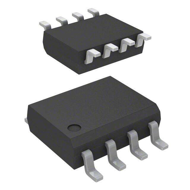
PG-DSO-8
General Description
The TLF2931 is a positive voltage regulator with a very low quiescent current of 1mA or less when supplying
10 mA loads. The TLF2931GV50 provides an extremely low dropout voltage of less than 0.2 V for output currents
up to 10 mA. Therefore the TLF2931 is the ideal supply for standby power systems. It certainly can also be used
for any system demanding as much as 100 mA of output current. The AEC qualified device is designed to
withstand the harsh environment and operation conditions of automotive applications.
The TLF2931 is protected from reverse polarity condition and can withstand input voltages of 28 V continuously.
The TLF2931 cannot be harmed by temporary mirror-image insertion. Additional protection features such as
output current limitation and overtemperature shutdown are also implemented. The TLF2931 comes in an 8-lead
SMD package (PG-DSO-8).
Type
Package
Marking
TLF2931GV50
PG-DSO-8
TLF2931
TLF2931GV33
PG-DSO-8
F931V33
Data Sheet
2
Rev. 1.0, 2010-10-06
�TLF2931
Block Diagram
2
Block Diagram
Saturation
Control and
Protection
Circuit
Temperature
Sensor
Input
8
1
Control
Amplifier
Adjustment
Output
Buffer
Bandgap
Reference
2,3,6,7
GND
AEB01527
Figure 1
Data Sheet
Block Diagram
3
Rev. 1.0, 2010-10-06
�TLF2931
Pin Configuration
3
Pin Configuration
3.1
Pin Assignment
PG-DSO-8
OUT
GND
GND
n.c.
1
2
3
4
8
IN
7
6
5
GND
GND
n.c.
PINCONFIG_DSO-8.VSD
Figure 2
Pin Configuration
3.2
Pin Definitions and Functions TLF2931GV50, TLF2931GV33 (PG-DSO-8)
Pin
Symbol
Function
1
OUT
Output
block to GND with a capacitor close to the IC terminals, respecting the values given
for its capacitance COUT and ESR in “Typical Performance Characteristics” on
Page 9
2,3,6,7
GND
Ground
4,5
n.c.
not connected
8
IN
Input
for compensating line influences, a capacitor to GND close to the IC terminals is
recommended
Data Sheet
4
Rev. 1.0, 2010-10-06
�TLF2931
General Product Characteristics
4
General Product Characteristics
4.1
Absolute Maximum Ratings
Absolute Maximum Ratings 1)
Tj = -40 °C to 125 °C; all voltages with respect to ground, positive current flowing into pin
(unless otherwise specified)
Pos.
Parameter
Symbol
Limit Values
Min.
Max.
Unit
Conditions
Input
4.1.1
Voltage
VI
-30
42
V
–
Voltage
VOUT
-0.3
28
V
–
Tj
Tstg
-40
125
°C
–
-55
150
°C
–
VESD
VESD
-2
2
kV
HBM2)
-1
1
kV
CDM3)
Output
4.1.2
Temperatures
4.1.3
Junction Temperature
4.1.4
Storage Temperature
ESD Susceptibility
4.1.5
ESD Resistivity to GND
4.1.6
ESD Resistivity to GND
1) Not subject to production test, specified by design.
2) ESD susceptibility, HBM according to EIA/JESD 22-A114B
3) ESD susceptibility, Charged Device Model “CDM” ESDA STM5.3.1
Note: Stresses above the ones listed here may cause permanent damage to the device. Exposure to absolute
maximum rating conditions for extended periods may affect device reliability.
Note: Integrated protection functions are designed to prevent IC destruction under fault conditions described in the
data sheet. Fault conditions are considered as “outside” normal operating range. Protection functions are
not designed for continuous repetitive operation.
4.2
Pos.
4.2.1
Functional Range
Parameter
Input Voltage
Symbol
VI
4.2.2
4.2.3
Junction Temperature
Tj
Limit Values
Unit
Conditions
Min.
Max.
6
28
V
TLF2931GV50
4.4
26
V
TLF2931GV33
-40
125
°C
–
Note: Within the functional range the IC operates as described in the circuit description. The electrical
characteristics are specified within the conditions given in the related electrical characteristics table.
Data Sheet
5
Rev. 1.0, 2010-10-06
�TLF2931
General Product Characteristics
4.3
Pos.
Thermal Resistance
Parameter
Symbol
Limit Values
Min.
Typ.
Max.
Unit
Conditions
TLF2931GV50, TLF2931GV33 (PG-DSO-8)
4.3.1
Junction to Soldering Point1)
RthJSP
–
39
–
K/W
measured to group
of pins 2, 3, 6, 7
4.3.2
Junction to Ambient1)
RthJA
–
96
–
K/W
Footprint only2)
4.3.3
–
67
–
K/W
300mm2 heatsink
area on PCB2)
4.3.4
–
66
–
K/W
600mm2 heatsink
area on PCB2)
1) not subject to production test, specified by design
2) Specified RthJA value is according to Jedec JESD51-2,-7 at natural convection on FR4 2s2p board; The Product
(Chip + Package) was simulated on a 76.2 x 114.3 x 1.5 mm board with 2 inner copper layers (2 x 70µm Cu, 2 x 35µm Cu).
Data Sheet
6
Rev. 1.0, 2010-10-06
�TLF2931
Electrical Characteristics
5
Electrical Characteristics
5.1
Electrical Characteristics TLF2931GV50
Electrical Characteristics
VI = 14 V, Tj = -40 °C to 125 °C, IOUT = 10 mA, all voltages with respect to ground, positive current flowing into pin
(unless otherwise specified)
Pos.
Parameter
Symbol
5.1.1
Output Voltage
VOUT
5.1.2
Line Regulation
ΔVOUT,line
Load Regulation
1)
Min.
Typ.
Max.
4.75
5
5.25
Unit
Conditions
V
Tj = 25 °C
4.5
5
5.5
V
–
–
2
10
mV
9 V < VI < 16 V
–
4
30
mV
6 V < VI < 26 V
ΔVOUT,load
–
-14
-50
mV
5 mA < IOUT < 100 mA
ZOUT
–
200
–
mΩ
IOUT = 100 mADC and
IOUT = 10 mArms
–
0.4
1
mA
–
9
15
mA
–
500
–
µVrms
5.1.3
5.1.4
Limit Values
5.1.5
Output Impedance
5.1.6
Current Consumption
Iq
5.1.8
Output Noise Voltage1)
Vnoise
5.1.9
Long Term Stability1)
ΔVOUT,1000h –
20
–
mV
–
/1000h
5.1.10
Ripple Rejection1)
80
–
dB
fripple = 120 Hz
5.1.11
PSRR
VDR
–
2)
–
0.05
0.2
V
–
0.3
0.6
V
IOUT = 10 mA
IOUT = 100 mA
100 Hz - 10 kHz
5.1.7
5.1.12
Dropout Voltage
VI - VOUT
IOUT = 10 mA
6 V < VI < 26 V
IOUT = 100 mA
100 Hz - 10 kHz
COUT = 100 µF
1) Not subject to production test, specified by design
2) Obtained when the output voltage has dropped 100mV below the nominal value
Data Sheet
7
Rev. 1.0, 2010-10-06
�TLF2931
Electrical Characteristics
5.2
Electrical Characteristics TLF2931GV33
Electrical Characteristics
VI = 14 V, Tj = -40 °C to 125 °C, IOUT = 10 mA, all voltages with respect to ground, positive current flowing into pin
(unless otherwise specified)
Pos.
Parameter
Symbol
5.2.1
Output Voltage
VOUT
Limit Values
Unit
Conditions
Tj = 25 °C
4.4 V < VI < 26 V
IOUT = 100 mA
4.4 V < VI < 26 V
Tj = 25 °C
5 mA < IOUT < 100 mA
Tj = 25 °C
IOUT = 100 mADC and
IOUT = 10 mArms
Min.
Typ.
Max.
3.135
3.3
3.465
V
2.97
3.3
3.63
V
5.2.2
Line Regulation
ΔVOUT,line
–
4
33
mV
5.2.3
Load Regulation
ΔVOUT,load
–
-10
-50
mV
5.2.4
Output Impedance1)
ZOUT
–
200
–
mΩ
100 Hz - 10 kHz
5.2.5
Iq
Current Consumption
5.2.6
1)
Vnoise
–
0.4
1
mA
IOUT = 10 mA
4.4 V < VI < 26 V
–
9
15
mA
IOUT = 100 mA
–
330
–
µVrms
10 Hz - 100 kHz
COUT = 100 µF
5.2.7
Output Noise Voltage
5.2.8
Long Term Stability1)
ΔVOUT,1000h –
13
–
mV
–
/1000h
5.2.9
Ripple Rejection1)
PSRR
VDR
–
80
–
dB
fripple = 120 Hz
–
0.85
1.1
V
IOUT = 100 mA,
Tj = 25 °C
5.2.10
Dropout Voltage
VI - VOUT
2)
1) Not subject to production test, specified by design
2) Obtained when the output voltage has dropped 100mV below the nominal value
Data Sheet
8
Rev. 1.0, 2010-10-06
�TLF2931
Electrical Characteristics
5.3
Typical Performance Characteristics
Dropout Voltage VDR versus
Output Current IOUT
TLF2931GV50: Output Voltage VOUT versus
Input Voltage VI
AED01978
800
V DR mV
700
AED01984
6
VQ
V
R L = 50 Ω
5
600
4
500
Tj = 125 C
400
3
300
2
200
Tj = 25 C
1
100
0
25
75
50
100
125
mA
0
175
0
2
4
8
6
ΙQ
TLF2931GV33: Output Voltage VOUT versus
Input Voltage VI
Load Transient Response
V33_VQ _VI .VSD
3,5
ΔV OUT [mV]
3,0
I Q = 50 mA
2,5
2,0
20
C OUT = 100 µF
ESR(C OUT) = 0.4 Ω
0
-20
-40
-60
-80
1,5
[mA]
VQ [V]
LOADTRANSIENTRESPONSE.VSD
60
40
Ι OUT
1,0
0,5
0,0
0
2
4
6
8
160
140
120
100
80
60
40
20
0
-10 0
10
V I [V]
Data Sheet
V 10
VΙ
10 20 30 40 50 60 70 80 90
t [µs]
9
Rev. 1.0, 2010-10-06
�TLF2931
Electrical Characteristics
TLF2931GV50: Output Voltage VOUT versus
Junction Temperature Tj
TLF2931GV33: Output Voltage VOUT versus
Junction Temperature Tj
AED01982
5.20
V33_VQ_TJ.VSD
3,50
V
VQ
3,40
5.10
V I = 14 V
Vi = 13.5 V
3,30
V Q [V]
5.00
4.90
3,20
3,10
4.80
3,00
4.70
2,90
4.60
-40
0
40
80
-40
120 C 160
Tj
Output Current IOUT versus
Input Voltage VI
10
60
110
160
T j [°C]
Current Consumption Iq versus
Low Output Current IOUT
AED01983
200
AED01981
3.0
Ι Q mA
Ι q mA
2.5
150
2.0
Tj = 25 C
100
1.5
Tj = 125 C
1.0
Vi = 13.5 V
50
0.5
0
0
10
20
30
0
40 V 50
VΙ
Data Sheet
10
0
5
10
15
20
30
mA
ΙQ
Rev. 1.0, 2010-10-06
�TLF2931
Electrical Characteristics
Current Consumption Iq versus
Output Current IOUT
Current Consumption Iq versus
Input Voltage VI
AED01980
12
IQ_VI.VSD
12
Ι q mA
10
10
R
I q [mA]
Vi = 13.5 V
6
6
4
4
R
L
= 100 Ω
2
2
0
0
50
100
mA
0
150
ΙQ
Data Sheet
= 50 Ω
8
8
0
L
10
20
30
40
V I [V]
11
Rev. 1.0, 2010-10-06
�TLF2931
Electrical Characteristics
Power Supply Ripple Rejection PSRR versus
Frequency f
90,00
TLF2931GV50: Output Capacitor’s Equivalent
Series Resistance ESR(COUT) versus Output
Current IOUT
ESR_IOUT.VSD
10,00
PSRR_F.VSD
9,00
80,00
Unstable
Region
I OUT = 1 mA
8,00
70,00
C OUT = 10 µF
I OUT = 10 mA
) [Ω]
OUT
50,00
ESR(C
PSRR [dB]
60,00
7,00
I OUT = 100 mA
40,00
30,00
6,00
5,00
Stable Region
4,00
3,00
C OUT = 10 µF
ESR(C OUT ) = 0,02 Ω
20,00
2,00
10,00
1,00
0,00
0,01
0,00
0,1
1
10
0
100
20
40
60
80
100
I OUT [mA]
f [kHz]
TLF2931GV33: Output Capacitor’s Equivalent
Series Resistance ESR(COUT) versus Output
Current IOUT
V33_ESR_IOUT.VSD
10,00
9,00
Unstable
Region
8,00
ESR(C
OUT
) [Ω ]
7,00
6,00
5,00
C OUT = 10 µF
4,00
3,00
Stable Region
2,00
1,00
0,00
0
20
40
60
80
100
I OUT [mA]
Data Sheet
12
Rev. 1.0, 2010-10-06
�TLF2931
Package Outlines
6
Package Outlines
0.1
2)
0.41+0.1
-0.06
0.2
8
5
1
4
5 -0.2 1)
M
B
0.19 +0.06
C
8 MAX.
1.27
4 -0.21)
1.75 MAX.
0.175 ±0.07
(1.45)
0.35 x 45˚
0.64 ±0.25
6 ±0.2
A B 8x
0.2
M
C 8x
A
Index Marking
1) Does not include plastic or metal protrusion of 0.15 max. per side
2) Lead width can be 0.61 max. in dambar area
GPS01181
Figure 3
PG-DSO-8
Green Product (RoHS compliant)
To meet the world-wide customer requirements for environmentally friendly products and to be compliant with
government regulations the device is available as a green product. Green products are RoHS-Compliant (i.e
Pb-free finish on leads and suitable for Pb-free soldering according to IPC/JEDEC J-STD-020).
For further information on alternative packages, please visit our website:
http://www.infineon.com/packages.
Data Sheet
13
Dimensions in mm
Rev. 1.0, 2010-10-06
�TLF2931
Revision History
7
Revision History
Revision
Date
Changes
1.0
2010-10-06
Data Sheet
Data Sheet
14
Rev. 1.0, 2010-10-06
�Edition 2010-10-06
Published by
Infineon Technologies AG
81726 Munich, Germany
© 2010 Infineon Technologies AG
All Rights Reserved.
Legal Disclaimer
The information given in this document shall in no event be regarded as a guarantee of conditions or
characteristics. With respect to any examples or hints given herein, any typical values stated herein and/or any
information regarding the application of the device, Infineon Technologies hereby disclaims any and all warranties
and liabilities of any kind, including without limitation, warranties of non-infringement of intellectual property rights
of any third party.
Information
For further information on technology, delivery terms and conditions and prices, please contact the nearest
Infineon Technologies Office (www.infineon.com).
Warnings
Due to technical requirements, components may contain dangerous substances. For information on the types in
question, please contact the nearest Infineon Technologies Office.
Infineon Technologies components may be used in life-support devices or systems only with the express written
approval of Infineon Technologies, if a failure of such components can reasonably be expected to cause the failure
of that life-support device or system or to affect the safety or effectiveness of that device or system. Life support
devices or systems are intended to be implanted in the human body or to support and/or maintain and sustain
and/or protect human life. If they fail, it is reasonable to assume that the health of the user or other persons may
be endangered.
�