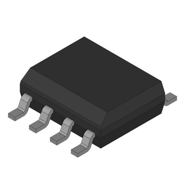
OPTIREG™ linear voltage regulator TLS115D0EJ
High-precision voltage tracker
Features
•
•
•
•
•
•
•
•
•
•
•
•
•
•
150 mA current capability
Very high tracking accuracy
Output voltage adjustable down to 2.0 V
Stable with ceramic output capacitors
Very low dropout voltage of typically 250 mV at 150 mA
Very low current consumption of typically 0.1 µA in standby mode
Overvoltage and undervoltage indication at power good output
Internally controlled soft start
Wide input voltage range: -16 V ≤ VIN ≤ 45 V
Wide temperature range: -40°C ≤ Tj ≤ 150°C
Short circuit protected output (to GND and to battery)
Reverse polarity protected input
Overtemperature protection
Green Product (RoHS compliant)
Potential applications
•
•
•
•
•
•
Automotive sensor supply
Protected sensor supply for off-board sensors
Secondary voltage supply in automotive ECU
High precision voltage tracking
Precision voltage replication
Power switch for off-board load
Product validation
Qualified for automotive applications. Product validation according to AEC-Q100.
Description
The OPTIREG™ linear voltage regulator TLS115D0EJ is a monolithic, integrated low-dropout voltage tracking
regulator with high accuracy in a small PG-DSO-8 package. The TLS115D0EJ is designed to supply off-board
systems, for example sensors in powertrain management systems under the severe conditions of automotive
applications. The TLS115D0EJ provides protection functions against reverse polarity as well as against short
circuit to GND and to battery. The output voltage follows the reference voltage that is applied to the ADJ input
Please read the sections "Important notice" and "Warnings" at the end of this document
Datasheet
www.infineon.com/OPTIREG-linear
Rev. 1.12
2022-11-10
�OPTIREG™ linear voltage regulator TLS115D0EJ
High-precision voltage tracker
Description
with very high accuracy up to a supply voltage of 45 V and up to an output current of 150 mA. The required
minimum reference voltage at ADJ is 2.0 V.
Type
Package
Marking
TLS115D0EJ
PG-DSO-8
115x0
Datasheet
2
Rev. 1.12
2022-11-10
�OPTIREG™ linear voltage regulator TLS115D0EJ
High-precision voltage tracker
Table of contents
Table of contents
Features . . . . . . . . . . . . . . . . . . . . . . . . . . . . . . . . . . . . . . . . . . . . . . . . . . . . . . . . . . . . . . . . . . . . . . . . . . . . . . . 1
Potential applications . . . . . . . . . . . . . . . . . . . . . . . . . . . . . . . . . . . . . . . . . . . . . . . . . . . . . . . . . . . . . . . . . . 1
Product validation . . . . . . . . . . . . . . . . . . . . . . . . . . . . . . . . . . . . . . . . . . . . . . . . . . . . . . . . . . . . . . . . . . . . . 1
Description . . . . . . . . . . . . . . . . . . . . . . . . . . . . . . . . . . . . . . . . . . . . . . . . . . . . . . . . . . . . . . . . . . . . . . . . . . . . 1
Table of contents . . . . . . . . . . . . . . . . . . . . . . . . . . . . . . . . . . . . . . . . . . . . . . . . . . . . . . . . . . . . . . . . . . . . . . . 3
1
Block diagram . . . . . . . . . . . . . . . . . . . . . . . . . . . . . . . . . . . . . . . . . . . . . . . . . . . . . . . . . . . . . . . . . . . . . . . . . 5
2
2.1
2.2
Pin configuration . . . . . . . . . . . . . . . . . . . . . . . . . . . . . . . . . . . . . . . . . . . . . . . . . . . . . . . . . . . . . . . . . . . . . . .6
Pin assignment . . . . . . . . . . . . . . . . . . . . . . . . . . . . . . . . . . . . . . . . . . . . . . . . . . . . . . . . . . . . . . . . . . . . . . . . . 6
Pin definitions and functions . . . . . . . . . . . . . . . . . . . . . . . . . . . . . . . . . . . . . . . . . . . . . . . . . . . . . . . . . . . . . 6
3
3.1
3.2
3.3
General product characteristics . . . . . . . . . . . . . . . . . . . . . . . . . . . . . . . . . . . . . . . . . . . . . . . . . . . . . . . . . 7
Absolute maximum ratings . . . . . . . . . . . . . . . . . . . . . . . . . . . . . . . . . . . . . . . . . . . . . . . . . . . . . . . . . . . . . . .7
Functional range . . . . . . . . . . . . . . . . . . . . . . . . . . . . . . . . . . . . . . . . . . . . . . . . . . . . . . . . . . . . . . . . . . . . . . . . 8
Thermal resistance . . . . . . . . . . . . . . . . . . . . . . . . . . . . . . . . . . . . . . . . . . . . . . . . . . . . . . . . . . . . . . . . . . . . . . 8
4
4.1
4.2
4.3
4.4
4.5
4.6
4.7
4.8
4.9
4.10
4.11
4.12
4.13
Block description and electrical characteristics . . . . . . . . . . . . . . . . . . . . . . . . . . . . . . . . . . . . . . . . .10
Functional description tracking regulator . . . . . . . . . . . . . . . . . . . . . . . . . . . . . . . . . . . . . . . . . . . . . . . . .10
Electrical characteristics tracking regulator . . . . . . . . . . . . . . . . . . . . . . . . . . . . . . . . . . . . . . . . . . . . . . . 11
Typical performance characteristics tracking regulator . . . . . . . . . . . . . . . . . . . . . . . . . . . . . . . . . . . . 13
Electrical characteristics current consumption . . . . . . . . . . . . . . . . . . . . . . . . . . . . . . . . . . . . . . . . . . . . 16
Typical performance characteristics current consumption . . . . . . . . . . . . . . . . . . . . . . . . . . . . . . . . . 17
Functional description enable input . . . . . . . . . . . . . . . . . . . . . . . . . . . . . . . . . . . . . . . . . . . . . . . . . . . . . 19
Electrical characteristics enable input . . . . . . . . . . . . . . . . . . . . . . . . . . . . . . . . . . . . . . . . . . . . . . . . . . . .19
Typical performance characteristics enable input . . . . . . . . . . . . . . . . . . . . . . . . . . . . . . . . . . . . . . . . . 20
Functional description adjust input . . . . . . . . . . . . . . . . . . . . . . . . . . . . . . . . . . . . . . . . . . . . . . . . . . . . . . 21
Electrical characteristics adjust input . . . . . . . . . . . . . . . . . . . . . . . . . . . . . . . . . . . . . . . . . . . . . . . . . . . . 21
Typical performance characteristics adjust input . . . . . . . . . . . . . . . . . . . . . . . . . . . . . . . . . . . . . . . . . . 22
Functional description power good output . . . . . . . . . . . . . . . . . . . . . . . . . . . . . . . . . . . . . . . . . . . . . . . 23
Electrical characteristics power good output . . . . . . . . . . . . . . . . . . . . . . . . . . . . . . . . . . . . . . . . . . . . . .23
5
5.1
5.2
5.2.1
5.2.2
5.2.3
5.2.4
5.3
5.4
Application information . . . . . . . . . . . . . . . . . . . . . . . . . . . . . . . . . . . . . . . . . . . . . . . . . . . . . . . . . . . . . . . 24
Application diagram . . . . . . . . . . . . . . . . . . . . . . . . . . . . . . . . . . . . . . . . . . . . . . . . . . . . . . . . . . . . . . . . . . . .24
Selection of external components . . . . . . . . . . . . . . . . . . . . . . . . . . . . . . . . . . . . . . . . . . . . . . . . . . . . . . . 24
Input pin . . . . . . . . . . . . . . . . . . . . . . . . . . . . . . . . . . . . . . . . . . . . . . . . . . . . . . . . . . . . . . . . . . . . . . . . . . . . 24
Output pin . . . . . . . . . . . . . . . . . . . . . . . . . . . . . . . . . . . . . . . . . . . . . . . . . . . . . . . . . . . . . . . . . . . . . . . . . . .25
Adjust pin . . . . . . . . . . . . . . . . . . . . . . . . . . . . . . . . . . . . . . . . . . . . . . . . . . . . . . . . . . . . . . . . . . . . . . . . . . . 25
Power good pin . . . . . . . . . . . . . . . . . . . . . . . . . . . . . . . . . . . . . . . . . . . . . . . . . . . . . . . . . . . . . . . . . . . . . . 25
Thermal considerations . . . . . . . . . . . . . . . . . . . . . . . . . . . . . . . . . . . . . . . . . . . . . . . . . . . . . . . . . . . . . . . . .25
Further application information . . . . . . . . . . . . . . . . . . . . . . . . . . . . . . . . . . . . . . . . . . . . . . . . . . . . . . . . . 26
6
Package information . . . . . . . . . . . . . . . . . . . . . . . . . . . . . . . . . . . . . . . . . . . . . . . . . . . . . . . . . . . . . . . . . . 27
Datasheet
3
Rev. 1.12
2022-11-10
�OPTIREG™ linear voltage regulator TLS115D0EJ
High-precision voltage tracker
Table of contents
Revision history . . . . . . . . . . . . . . . . . . . . . . . . . . . . . . . . . . . . . . . . . . . . . . . . . . . . . . . . . . . . . . . . . . . . . . .28
Disclaimer . . . . . . . . . . . . . . . . . . . . . . . . . . . . . . . . . . . . . . . . . . . . . . . . . . . . . . . . . . . . . . . . . . . . . . . . . . . . 29
Datasheet
4
Rev. 1.12
2022-11-10
�OPTIREG™ linear voltage regulator TLS115D0EJ
High-precision voltage tracker
1 Block diagram
1
Block diagram
OUT
IN
Protection
Circuits
Power
Good
EN
PG
ADJ
Enable
Temperature
Shutdown
GND
Figure 1
Datasheet
Block diagram
5
Rev. 1.12
2022-11-10
�OPTIREG™ linear voltage regulator TLS115D0EJ
High-precision voltage tracker
2 Pin configuration
2
Pin configuration
2.1
Pin assignment
OUT
1
8
IN
N.C.
2
7
EN
GND
3
6
N.C.
PG
4
5
ADJ
Figure 2
Pin Configuration
2.2
Pin definitions and functions
Pin
Symbol
Function
1
OUT
Tracker output:
150 mA output current capability.
Connect this pin to GND with a capacitor close to the pins, maintaining
capacitance and ESR requirements given in Table 2.
2
N.C.
Not connected
3
GND
Ground
4
PG
Power good:
Open drain output.
Connect this pin to a positive voltage rail via a pull-up resistor.
"Low" signal indicates a fault condition of the tracker output.
5
ADJ
Adjust:
Connect this pin to the reference voltage.
6
N.C.
Not connected
7
EN
Enable input:
"High" signal enables the tracker.
"Low" signal disables the tracker.
If the enable function is not required, then connect EN to IN.
8
IN
Input:
It is recommended to connect this pin to GND using a small ceramic capacitor
close to the pins in order to compensate line influence.
Pad
–
Exposed pad:
Connect the exposed pad to GND.It is recommended to connect the exposed pad
to a heat sink.
Datasheet
6
Rev. 1.12
2022-11-10
�OPTIREG™ linear voltage regulator TLS115D0EJ
High-precision voltage tracker
3 General product characteristics
3
General product characteristics
3.1
Absolute maximum ratings
Table 1
Absolute maximum ratings1)
Tj = -40°C to 150°C; all voltages with respect to ground, positive current flowing into pin
(unless otherwise specified)
Parameter
Symbol
Values
Min.
Typ.
Unit
Note or
condition
Number
Max.
Input IN
Voltage
VIN
-16
–
45
V
–
P_3.1.1
VEN
-16
–
45
V
–
P_3.1.2
VADJ
-16
–
45
V
–
P_3.1.3
VOUT
-5
–
45
V
–
P_3.1.4
VIN - VOUT
-30
–
45
V
–
P_3.1.5
VPG
-0.3
–
7
V
–
P_3.1.6
Junction temperature
Tj
-40
–
150
°C
–
P_3.1.7
Storage temperature
Tstg
-55
–
150
°C
–
P_3.1.8
ESD susceptibility to GND
VESD,HBM
-4
–
4
kV
2) Human Body
P_3.1.9
ESD susceptibility to GND
VESD,CDM
-1
–
1
kV
3) Charged Device
P_3.1.10
ESD susceptibility to GND
VESD,CDM
-1
–
1
kV
3) Charged Device
P_3.1.11
Enable EN
Voltage
Adjust ADJ
Voltage
Output OUT
Voltage
Input output voltage difference
Voltage
Power good PG
Voltage
Temperatures
ESD Susceptibility
1)
2)
3)
Model (HBM)
Model (CDM)
Model (CDM) at
corner pins
Not subject to production test, specified by design.
Human body model (HBM) robustness according to ANSI/ESDA/JEDEC JS-001 (1.5 kΩ, 100 pF).
Charged device model (CDM) robustness according to JEDEC JESD22-C101.
Notes:
Datasheet
7
Rev. 1.12
2022-11-10
�OPTIREG™ linear voltage regulator TLS115D0EJ
High-precision voltage tracker
3 General product characteristics
1.
2.
Stresses above the ones listed here may cause permanent damage to the device. Exposure to absolute
maximum rating conditions for extended periods of time may affect device reliability.
Integrated protection functions are designed to prevent IC destruction under fault conditions described in
the datasheet. Fault conditions are considered as outside the normal operating range. Protection functions
are not designed for continuous repetitive operation.
3.2
Functional range
Table 2
Functional range
Parameter
Symbol
Values
Min.
Typ.
Unit
Note or
condition
Number
Max.
Input voltage range
VIN
4
–
45
V
–
P_3.2.1
Adjust input voltage range
(voltage tracking range)
VADJ
2
–
14
V
–
P_3.2.2
Capacitance of output
capacitor
COUT
1
–
–
µF
1) 2)
P_3.2.3
Equivalent series resistance ESRCOUT
of output capacitor
–
–
5
Ω
2)
P_3.2.4
Junction temperature
-40
–
150
°C
–
P_3.2.5
1)
2)
Tj
The minimum output capacitance requirement is applicable for a worst case capacitance tolerance of 30%.
Not subject to production test, specified by design.
Note:
Within the functional range, the IC operates as described in the circuit description. The electrical
characteristics are specified within the conditions given in the electrical characteristics table.
3.3
Note:
Thermal resistance
This thermal data was generated in accordance with JEDEC JESD51 standards. For more information,
go to www.jedec.org.
Table 3
Thermal resistance
Parameter
Symbol
Values
Min.
Typ.
Unit
Note or condition
Number
Max.
Junction to case
RthJC
–
18
–
K/W
1)
P_3.3.1
Junction to pin
RthJP
–
85
–
K/W
–
P_3.3.2
Junction to ambient
RthJA
–
50
–
K/W
2) 2s2p board
P_3.3.3
Junction to ambient
RthJA
–
157
–
K/W
3) 1s0p board, footprint
P_3.3.4
Junction to ambient
RthJA
–
77
–
K/W
3) 1s0p board, 300 mm2
P_3.3.5
Junction to ambient
RthJA
–
63
–
K/W
3) 1s0p board, 600 mm2
P_3.3.6
only
heatsink area on PCB
heatsink area on PCB
(table continues...)
Datasheet
8
Rev. 1.12
2022-11-10
�OPTIREG™ linear voltage regulator TLS115D0EJ
High-precision voltage tracker
3 General product characteristics
Table 3
Parameter
(continued) Thermal resistance
Symbol
Values
Min.
1)
2)
3)
Typ.
Unit
Note or condition
Number
Max.
Not subject to production test, specified by design.
Specified RthJA value is according to JEDEC JESD51-2,-5,-7 at natural convection on FR4 2s2p board; the product (chip and
package) was simulated on a 76.2 × 114.3 × 1.5 mm3 board with two inner copper layers (2 × 70 µm Cu, 2 × 35 µm Cu). Where
applicable, a thermal via array next to the package contacted the first inner copper layer.
Specified RthJA value is according to JEDEC JESD51-3 at natural convection on FR4 1s0p board; the product (chip and package)
was simulated on a 76.2 × 114.3 × 1.5 mm3 board with one copper layer (1 × 70 µm Cu).
Note:
Datasheet
This thermal data was generated in accordance with JEDEC JESD51 standards. For more information
visit www.jedec.org.
9
Rev. 1.12
2022-11-10
�OPTIREG™ linear voltage regulator TLS115D0EJ
High-precision voltage tracker
4 Block description and electrical characteristics
4
Block description and electrical characteristics
4.1
Functional description tracking regulator
The regulator controls the output voltage VOUT by comparing it to the voltage applied to the ADJ pin and driving
a PNP pass transistor accordingly. The stability of the control loop depends on:
•
The output capacitor COUT
•
Load current
•
Chip temperature
•
The poles and zeroes in the frequency response of the circuit consisting of the TLS115D0EJ and the load
An input capacitor CIN is strongly recommended for buffering the line influence.
To ensure stable operation, the output capacitor’s capacitance and its equivalent series resistance ESR must
fulfill the requirements in Table 2. The output capacitor must be sized suitably to buffer load transients.
Connect each capacitor close to the pins.
The internal protection features are designed to protect the device itself as well as the application from
destruction in case of catastrophic events. These safeguards contain:
•
Output current limitation
• Reverse polarity protection
• Thermal shutdown
Output current limitation
In order to protect the pass element and the package from excessive power dissipation, the device limits the
maximum output current at high input voltage.
Reverse polarity protection
The device allows a negative supply voltage. However, in reverse polarity condition several small currents
flowing into the device increase the junction temperature. Thermal design must consider this effect, because in
reverse polarity condition the overtemperature protection circuit does not operate.
Thermal shutdown
The overtemperature protection circuit is designed to prevent immediate destruction of the device in certain
fault conditions (for example a permanent short circuit at output) by switching off the power stage. After the
chip cools down, the regulator restarts. If the fault is not removed, then this leads to an oscillatory behavior
of the output voltage. A junction temperature above 150°C is outside the maximum ratings and reduces the
lifetime of the device.
Datasheet
10
Rev. 1.12
2022-11-10
�OPTIREG™ linear voltage regulator TLS115D0EJ
High-precision voltage tracker
4 Block description and electrical characteristics
4.2
Electrical characteristics tracking regulator
Table 4
Electrical characteristics tracking regulator
VIN = 13.5 V; 2.0 V ≤ VADJ ≤ 14 V; VEN ≥ 2.0 V; Tj = -40°C to 150°C; all voltages with respect to ground, positive
current flowing into pin (unless otherwise specified).
Parameter
Symbol
Values
Min.
Typ.
Unit
Note or condition
Number
Max.
Tracking output
Output voltage tracking
accuracy
∆VOUT
-5
–
5
mV
∆VOUT = VADJ - VOUT;
5.5 V ≤ VIN ≤ 22 V;
0.1 mA ≤ IOUT ≤
150 mA;
2 V ≤ VADJ ≤ VIN - 1 V
P_4.1.1
Output voltage tracking
accuracy
∆VOUT
-5
–
5
mV
∆VOUT = VADJ - VOUT;
5.5 V ≤ VIN ≤ 32 V;
0.1 mA ≤ IOUT ≤
70 mA;
2 V ≤ VADJ ≤ VIN - 1 V
P_4.1.2
Load regulation steady-state ∆VOUT,load
-4
-0.1
–
mV
IOUT = 0.1 mA to
150 mA;
VADJ = 5 V
P_4.1.3
Line regulation steady-state
∆VOUT,line
–
0.1
4
mV
VIN = 5.5 V to 32 V;
IOUT = 10 mA;
VADJ = 5 V
P_4.1.4
Power supply ripple
rejection
PSRR
–
85
–
dB
1) f
P_4.1.5
Output current limitation
IOUT,max
151
350
500
mA
VOUT = VADJ - 0.1 V;
VADJ = 5 V
P_4.1.6
Reverse current
IOUT,rev
-3.5
-1.7
–
mA
VIN = 0 V;
VOUT = 16 V;
VADJ = 5 V
P_4.1.9
Reverse current at negative
input voltage
IIN,rev
-4
-2
–
mA
VIN = -16 V;
VOUT = 0 V;
VADJ = 5 V
P_4.1.10
Dropout voltage
Vdr
–
250
500
mV
2) V
P_4.1.11
ripple = 100 Hz;
Vripple = 1 Vpp;
IOUT = 10 mA;
COUT = 10 μF,
ceramic type
dr = VIN - VOUT;
IOUT = 150 mA;
VADJ = 5 V
(table continues...)
Datasheet
11
Rev. 1.12
2022-11-10
�OPTIREG™ linear voltage regulator TLS115D0EJ
High-precision voltage tracker
4 Block description and electrical characteristics
Table 4
(continued) Electrical characteristics tracking regulator
VIN = 13.5 V; 2.0 V ≤ VADJ ≤ 14 V; VEN ≥ 2.0 V; Tj = -40°C to 150°C; all voltages with respect to ground, positive
current flowing into pin (unless otherwise specified).
Parameter
Symbol
Values
Min.
Typ.
Unit
Note or condition
Number
Max.
Overtemperature protection
Overtemperature shutdown
threshold
Tj,sd
–
175
–
°C
Tj increasing due
P_4.1.15
to power dissipation
generated by the
device
Overtemperature shutdown
threshold hysteresis
∆Tj,sdh
–
15
–
K
–
1)
2)
P_4.1.16
Not subject to production test, specified by design.
Measured when the output voltage VOUT has dropped 100 mV from the nominal value obtained at VIN = 13.5 V.
Datasheet
12
Rev. 1.12
2022-11-10
�OPTIREG™ linear voltage regulator TLS115D0EJ
High-precision voltage tracker
4 Block description and electrical characteristics
4.3
Typical performance characteristics tracking regulator
Tracking accuracy ΔVOUT versus
junction temperature Tj
Output current limitation IOUT,max versus
input voltage VIN
Output voltage VOUT versus
adjust voltage VADJ
Output voltage VOUT versus
input voltage VIN
Datasheet
13
Rev. 1.12
2022-11-10
�OPTIREG™ linear voltage regulator TLS115D0EJ
High-precision voltage tracker
4 Block description and electrical characteristics
Load regulation ΔVOUT,load versus
output current IOUT
Line regulation ΔVOUT,line versus
input voltage VIN
Dropout voltage Vdr versus
junction temperature Tj
Dropout voltage Vdr versus
output current IOUT
Datasheet
14
Rev. 1.12
2022-11-10
�OPTIREG™ linear voltage regulator TLS115D0EJ
High-precision voltage tracker
4 Block description and electrical characteristics
Reverse current IIN,rev versus
input voltage VIN
Reverse current IOUT,rev versus
output voltage VOUT
Power supply ripple rejection PSRR versus
ripple frequency fr
Output capacitor ESRCOUT versus
output current IOUT
Datasheet
15
Rev. 1.12
2022-11-10
�OPTIREG™ linear voltage regulator TLS115D0EJ
High-precision voltage tracker
4 Block description and electrical characteristics
4.4
Electrical characteristics current consumption
Table 5
Electrical characteristics current consumption
VIN = 13.5 V; 2.0 V ≤ VADJ ≤ 14 V; VEN ≥ 2.0 V; Tj = -40°C to 150°C; all voltages with respect to ground, positive
current flowing into pin (unless otherwise specified).
Parameter
Symbol
Values
Min.
Typ.
Unit
Note or condition
Number
Max.
Current consumption stand- Iq,off
by mode
–
0.1
5
µA
Iq,off = IIN;
VEN ≤ 0.4 V;
Tj ≤ 125°C
P_4.3.1
Current consumption
Iq
–
55
90
µA
Iq = IIN - IOUT;
IOUT ≤ 0.1 mA;
VADJ = 5 V;
Tj ≤ 125 °C
P_4.3.2
Current consumption
Iq
–
7
14
mA
Iq = IIN - IOUT;
IOUT ≤ 150 mA;
VADJ = 5 V
P_4.3.3
Datasheet
16
Rev. 1.12
2022-11-10
�OPTIREG™ linear voltage regulator TLS115D0EJ
High-precision voltage tracker
4 Block description and electrical characteristics
4.5
Typical performance characteristics current consumption
Current consumption Iq versus
output current IOUT
Current consumption Iq versus
input voltage VIN
Current consumption Iq versus
junction temperature Tj
Current consumption Iq versus
junction temperature Tj (IOUT low)
Datasheet
17
Rev. 1.12
2022-11-10
�OPTIREG™ linear voltage regulator TLS115D0EJ
High-precision voltage tracker
4 Block description and electrical characteristics
Current consumption in off-mode Iq,off versus
junction temperature Tj
Datasheet
18
Rev. 1.12
2022-11-10
�OPTIREG™ linear voltage regulator TLS115D0EJ
High-precision voltage tracker
4 Block description and electrical characteristics
4.6
Functional description enable input
On a "low" signal at the enable input EN the device switches to standby mode in order to minimize the
quiescent current.
If the EN pin is not connected, then the "low" level from the internal pull-down resistor switches off the
regulator.
4.7
Electrical characteristics enable input
Table 6
Electrical characteristics enable input
VIN = 13.5 V; 2.0 V ≤ VADJ ≤ 14 V; Tj = -40°C to 150°C; all voltages with respect to ground, positive current flowing
into pin (unless otherwise specified).
Parameter
Symbol
Values
Min.
Typ.
Unit
Note or
condition
Number
Max.
Enable off voltage range
VEN,off
–
–
0.8
V
VOUT = 0 V;
IOUT ≤ 5 μA;
Tj ≤ 125°C
P_4.5.1
Enable on voltage range
VEN,on
2
–
–
V
VOUT settled
P_4.5.2
Enable input current
IEN
–
2
4
µA
VEN = 5 V
P_4.5.3
Datasheet
19
Rev. 1.12
2022-11-10
�OPTIREG™ linear voltage regulator TLS115D0EJ
High-precision voltage tracker
4 Block description and electrical characteristics
4.8
Typical performance characteristics enable input
Enable input current IEN versus
enable input voltage VEN
Datasheet
20
Rev. 1.12
2022-11-10
�OPTIREG™ linear voltage regulator TLS115D0EJ
High-precision voltage tracker
4 Block description and electrical characteristics
4.9
Functional description adjust input
The adjust input must be connected to the reference voltage that the device tracks.
4.10
Electrical characteristics adjust input
Table 7
Electrical characteristics adjust input
VIN = 13.5 V; 2.0 V ≤ VADJ ≤ 14 V; VEN ≥ 2.0 V; Tj = -40°C to 150°C; all voltages with respect to ground, positive
current flowing into pin (unless otherwise specified).
Parameter
Symbol
Values
Min.
Adjust input current
Datasheet
IADJ
–
Unit
Typ.
0.03
21
Max.
1
μA
Note or
condition
Number
VADJ = 5 V
P_4.7.1
Rev. 1.12
2022-11-10
�OPTIREG™ linear voltage regulator TLS115D0EJ
High-precision voltage tracker
4 Block description and electrical characteristics
4.11
Typical performance characteristics adjust input
Adjust input current IADJ versus
adjust input voltage VADJ
Datasheet
Adjust input current IADJ versus
junction temperature Tj
22
Rev. 1.12
2022-11-10
�OPTIREG™ linear voltage regulator TLS115D0EJ
High-precision voltage tracker
4 Block description and electrical characteristics
4.12
Functional description power good output
The power good output PG indicates an overvoltage or undervoltage condition at the tracker output. For this
the device compares the output voltage VOUT to the reference voltage VADJ. The device indicates variations of
the output voltage beyond the power good switching thresholds by a "low" signal at the power good output
PG. Transients shorter than the power good reaction time tPG,r do not trigger the power good output.
4.13
Electrical characteristics power good output
The power good output PG is an open drain output that requires a pull-up resistor to a positive voltage rail.
The pull-up voltage must maintain the absolute maximum ratings of power good PG, see Absolute maximum
ratings.
Table 8
Electrical characteristics power good output
VIN = 13.5 V; 2.0 V ≤ VADJ ≤ 14 V; VEN ≥ 2.0 V; Tj = -40°C to 150°C; all voltages with respect to ground, positive
current flowing into pin (unless otherwise specified).
Parameter
Symbol
Values
Min.
Typ.
Unit
Note or condition
Number
Max.
Power good switching
threshold, undervoltage
VOUT,UV
VADJ 120
VADJ 70
VADJ 50
mV
VOUT decreasing;
VIN ≥ VAD + 150 mV
P_4.9.1
Power good switching
threshold, overvoltage
VOUT,OV
VADJ +
50
VADJ +
70
VADJ +
120
mV
VOUT increasing;
VIN ≥ VADJ + 150 mV
P_4.9.2
Power good reaction time
tPG,r
10
15
30
µs
–
P_4.9.3
Power good output "low"
voltage
VPG,low
–
0.2
0.4
V
VIN ≥ 4 V;
IPG,ext ≤ 1.8 mA
P_4.9.4
Power good output external
input current
IPG,ext
–
–
1.8
mA
VPG ≤ 0.4 V
P_4.9.5
Power good output leakage
current
IPG,leak
–
0
2
µA
VOUT = VADJ;
VPG = 5 V
P_4.9.6
Datasheet
23
Rev. 1.12
2022-11-10
�OPTIREG™ linear voltage regulator TLS115D0EJ
High-precision voltage tracker
5 Application information
5
Application information
Note:
The following information is given as an example for the implementation of the device only and shall
not be regarded as a description or warranty of a certain functionality, condition or quality of the
device.
5.1
Application diagram
VBAT
I
D1
Main
Regulator
VDD
Q
GND
Micro
Controller
I/O
I/O
RPG
EN
VREF
CIN2
Figure 3
Note:
CIN1
PG
ADJ TLS115D0
OUT
IN
GND
COUT
e.g. off board
loads, sensors
Application diagram
This figure is a simplified example of an application circuit. The function must be verified in the
application.
5.2
Selection of external components
5.2.1
Input pin
Figure 3 shows the typical input circuitry for a voltage tracking regulator. The following external components at
the input are recommended in case of possible external disturbance.
Ceramic capacitor
A ceramic capacitor CIN1 (100 nF to 470 nF) at the input filters high frequency disturbance imposed by the line,
such as ISO pulses 3a/b. Place CIN1 as close as possible to the input pin of the voltage tracking regulator on the
PCB.
Aluminum electrolytic capacitor
An aluminum electrolytic capacitor CIN2 (10 µF to 470 µF) at the input smoothens high energy pulses, such as
ISO pulse 2a. Place CIN2 close to the input pin of the voltage tracking regulator on the PCB.
Datasheet
24
Rev. 1.12
2022-11-10
�OPTIREG™ linear voltage regulator TLS115D0EJ
High-precision voltage tracker
5 Application information
Overvoltage suppression diode
A suitably sized diode D1 suppresses high voltage beyond the maximum ratings of the circuit components and
protects the device from damage due to overvoltage.
5.2.2
Output pin
An output capacitor COUT is necessary for the stability of the voltage tracking regulator, see Functional
range. The typical performance graph Output capacitor ESRCOUT versusoutput current IOUT shows the stable
operation range of the device.
In an automotive environment, ceramic capacitors with X5R or X7R dielectrics are recommended.
Place COUT on the same side of the PCB as the device and as close as possible to both the OUTpin and the GND
pin.
In case of rapid transients of input voltage or load current, COUT must be dimensioned accordingly to ensure the
output stability in the application.
5.2.3
Adjust pin
Figure 3 shows a typical adjust circuitry for a voltage tracking regulator. Typically the adjust pin is connected to
a fixed voltage reference that the regulator tracks. In the example of the application diagram ADJ is connected
to the supply voltage of a microcontroller. Alternatively, the voltage reference can also be adjusted by a voltage
divider.
5.2.4
Power good pin
The power good output is an open drain output, which requires a pull-up resistor to a positive voltage rail. The
pull-up voltage at PG must maintain the values specified in Absolute maximum ratings. The example in Figure 3
uses the supply voltage VDD of a microcontroller as pull-up.
To limit the external input current according to the requirements in Electrical characteristics power good
output, the pull-up resistor must be sized depending on the pull-up voltage.
5.3
Thermal considerations
From the known input voltage, the output voltage and the load profile of the application, the total power
dissipation can be calculated:
PD = V IN − V OUT × I OUT + V IN × I q
Equation 1
with
•
PD: continuous power dissipation
•
VIN: input voltage
•
VOUT: output voltage
•
IOUT: output current
•
Iq: quiescent current
The maximum acceptable thermal resistance RthJA can then be calculated:
Datasheet
25
Rev. 1.12
2022-11-10
�OPTIREG™ linear voltage regulator TLS115D0EJ
High-precision voltage tracker
5 Application information
RthJA, max =
Equation 2
Tj, max − Ta
PD
with
•
Tj,max: maximum allowed junction temperature
•
Ta: ambient temperature
Based on the above calculation the proper PCB type and the necessary heat sink area can be determined with
reference to the specification in Thermal resistance.
Example
Application conditions:
VIN = 13.5 V
VOUT = VADJ = 5 V
IOUT = 100 mA
Ta = 75°C
Calculation of RthJA,max:
PD = (VIN – VOUT) × IOUT + VIN × Iq
= (13.5V – 5V) × 100 mA + 13.5 V × 3.5 mA
= 0.897 W
RthJA,max = (Tj,max – Ta) / PD
= (150°C – 75°C) / 0.897 W
= 83.6 K/W
As a result, the PCB design must ensure a thermal resistance RthJA lower than 83.6 K/W. According to Thermal
resistance, at least 300 mm² heat sink area is required on the FR4 1s0p PCB, or the FR4 2s2p board can be used.
5.4
•
Further application information
For further information you may contact http://www.infineon.com/
Datasheet
26
Rev. 1.12
2022-11-10
�OPTIREG™ linear voltage regulator TLS115D0EJ
High-precision voltage tracker
6 Package information
2x
0.35x45°
0.64±0.25
Seating Plane
0.08 C
Coplanarity
1.27
D
6±0.2
A
0.2
D 8x
Bottom View
5
5
8
4
4
1
2.65±0.2
8
0.1 C D 2x
8° MAX.
0.1 C A-B
1)
3.9±0.1
0.19+0.06
(1.45)
1)
4.9±0.1
1.7 Max.
Package information
0..0.1
Stand Off
6
1
B
Index
Marking
0.41±0.09
3±0.2
2)
0.2
C A-B D 8x
1) Does not include plastic or metal protrusion of 0.15max. per side
2) Dambar protrusion shall be maximum 0.1mm total in excess of lead width
All dimensions are in units mm
The drawing is in compliance with ISO 128-30, Projection Method 1 [
Figure 4
]
PG-DSO-8
Green Product (RoHS compliant)
To meet the world-wide customer requirements for environmentally friendly products and to be compliant
with government regulations the device is available as a Green Product. Green Products are RoHS compliant
(Pb-free finish on leads and suitable for Pb-free soldering according to IPC/JEDEC J-STD-020).
Information on alternative packages
Please visit www.infineon.com/packages.
Datasheet
27
Rev. 1.12
2022-11-10
�OPTIREG™ linear voltage regulator TLS115D0EJ
High-precision voltage tracker
Revision history
Revision history
Revision
Date
Changes
1.12
2022-11-10
Datasheet updated
• Editorial changes
1.11
2021-05-28
Datasheet updated
• Editorial changes
1.1
2020-03-19
Datasheet updated
• P_3.1.5 maximum value for input output voltage difference added
• Editorial changes
1.0
2016-10-13
Datasheet created
Datasheet
28
Rev. 1.12
2022-11-10
�Trademarks
All referenced product or service names and trademarks are the property of their respective owners.
Edition 2022-11-10
Published by
Infineon Technologies AG
81726 Munich, Germany
© 2022 Infineon Technologies AG
All Rights Reserved.
Do you have a question about any
aspect of this document?
Email: erratum@infineon.com
Document reference
IFX-Z8F55515726
Important notice
The information given in this document shall in no
event be regarded as a guarantee of conditions or
characteristics (“Beschaffenheitsgarantie”).
With respect to any examples, hints or any typical
values stated herein and/or any information regarding
the application of the product, Infineon Technologies
hereby disclaims any and all warranties and liabilities
of any kind, including without limitation warranties of
non-infringement of intellectual property rights of any
third party.
In addition, any information given in this document is
subject to customer’s compliance with its obligations
stated in this document and any applicable legal
requirements, norms and standards concerning
customer’s products and any use of the product of
Infineon Technologies in customer’s applications.
The data contained in this document is exclusively
intended for technically trained staff. It is the
responsibility of customer’s technical departments to
evaluate the suitability of the product for the intended
application and the completeness of the product
information given in this document with respect to such
application.
Warnings
Due to technical requirements products may contain
dangerous substances. For information on the types
in question please contact your nearest Infineon
Technologies office.
Except as otherwise explicitly approved by Infineon
Technologies in a written document signed by
authorized representatives of Infineon Technologies,
Infineon Technologies’ products may not be used in
any applications where a failure of the product or
any consequences of the use thereof can reasonably
be expected to result in personal injury.
�