Low Dropout Linear Voltage Regulator
TLS850D0TA
TLS850D0TAV50
TLS850D0TAV33
Linear Voltage Regulator
Data Sheet
Rev. 1.0, 2015-12-01
Automotive Power
�TLS850D0TA
Table of Contents
Table of Contents
1
Overview . . . . . . . . . . . . . . . . . . . . . . . . . . . . . . . . . . . . . . . . . . . . . . . . . . . . . . . . . . . . . . . . . . . . . . . 3
2
Block Diagram . . . . . . . . . . . . . . . . . . . . . . . . . . . . . . . . . . . . . . . . . . . . . . . . . . . . . . . . . . . . . . . . . . . 5
3
3.1
3.2
Pin Configuration . . . . . . . . . . . . . . . . . . . . . . . . . . . . . . . . . . . . . . . . . . . . . . . . . . . . . . . . . . . . . . . . 6
Pin Assignment TLS850D0TAV50 and TLS850D0TAV33 . . . . . . . . . . . . . . . . . . . . . . . . . . . . . . . . . . 6
Pin Definitions and Functions TLS850D0TAV50 and TLS850D0TAV33 . . . . . . . . . . . . . . . . . . . . . . . 6
4
4.1
4.2
4.3
General Product Characteristics . . . . . . . . . . . . . . . . . . . . . . . . . . . . . . . . . . . . . . . . . . . . . . . . . . . .
Absolute Maximum Ratings . . . . . . . . . . . . . . . . . . . . . . . . . . . . . . . . . . . . . . . . . . . . . . . . . . . . . . . . .
Functional Range . . . . . . . . . . . . . . . . . . . . . . . . . . . . . . . . . . . . . . . . . . . . . . . . . . . . . . . . . . . . . . . . .
Thermal Resistance . . . . . . . . . . . . . . . . . . . . . . . . . . . . . . . . . . . . . . . . . . . . . . . . . . . . . . . . . . . . . . .
5
5.1
5.2
5.3
5.4
5.5
5.6
5.7
5.8
Block Description and Electrical Characteristics . . . . . . . . . . . . . . . . . . . . . . . . . . . . . . . . . . . . .
Voltage Regulation . . . . . . . . . . . . . . . . . . . . . . . . . . . . . . . . . . . . . . . . . . . . . . . . . . . . . . . . . . . . . . .
Typical Performance Characteristics Voltage Regulator . . . . . . . . . . . . . . . . . . . . . . . . . . . . . . . . . .
Current Consumption . . . . . . . . . . . . . . . . . . . . . . . . . . . . . . . . . . . . . . . . . . . . . . . . . . . . . . . . . . . . .
Typical Performance Characteristics Current Consumption . . . . . . . . . . . . . . . . . . . . . . . . . . . . . . . .
Enable . . . . . . . . . . . . . . . . . . . . . . . . . . . . . . . . . . . . . . . . . . . . . . . . . . . . . . . . . . . . . . . . . . . . . . . . .
Typical Performance Characteristics Enable . . . . . . . . . . . . . . . . . . . . . . . . . . . . . . . . . . . . . . . . . . .
Reset . . . . . . . . . . . . . . . . . . . . . . . . . . . . . . . . . . . . . . . . . . . . . . . . . . . . . . . . . . . . . . . . . . . . . . . . .
Typical Performance Characteristics Reset . . . . . . . . . . . . . . . . . . . . . . . . . . . . . . . . . . . . . . . . . . . .
10
10
13
16
17
18
19
20
25
6
6.1
6.2
6.2.1
6.2.2
6.3
6.4
6.5
Application Information . . . . . . . . . . . . . . . . . . . . . . . . . . . . . . . . . . . . . . . . . . . . . . . . . . . . . . . . . .
Application Diagram . . . . . . . . . . . . . . . . . . . . . . . . . . . . . . . . . . . . . . . . . . . . . . . . . . . . . . . . . . . . . .
Selection of External Components . . . . . . . . . . . . . . . . . . . . . . . . . . . . . . . . . . . . . . . . . . . . . . . . . . .
Input Pin . . . . . . . . . . . . . . . . . . . . . . . . . . . . . . . . . . . . . . . . . . . . . . . . . . . . . . . . . . . . . . . . . . . . . .
Output Pin . . . . . . . . . . . . . . . . . . . . . . . . . . . . . . . . . . . . . . . . . . . . . . . . . . . . . . . . . . . . . . . . . . . .
Thermal Considerations . . . . . . . . . . . . . . . . . . . . . . . . . . . . . . . . . . . . . . . . . . . . . . . . . . . . . . . . . . .
Reverse Polarity Protection . . . . . . . . . . . . . . . . . . . . . . . . . . . . . . . . . . . . . . . . . . . . . . . . . . . . . . . .
Further Application Information . . . . . . . . . . . . . . . . . . . . . . . . . . . . . . . . . . . . . . . . . . . . . . . . . . . . . .
26
26
26
26
26
27
28
28
7
Package Outlines . . . . . . . . . . . . . . . . . . . . . . . . . . . . . . . . . . . . . . . . . . . . . . . . . . . . . . . . . . . . . . . 29
8
Revision History . . . . . . . . . . . . . . . . . . . . . . . . . . . . . . . . . . . . . . . . . . . . . . . . . . . . . . . . . . . . . . . . 30
Data Sheet
2
7
7
8
9
Rev. 1.0, 2015-12-01
�Low Dropout Linear Voltage Regulator
1
TLS850D0TA
Overview
Features
•
Wide Input Voltage Range from 3.0 V to 40 V
•
Fixed Output Voltage 5 V or 3.3 V
•
Output Voltage Precision ≤ ±2 %
•
Output Current Capability up to 500 mA
•
Ultra Low Current Consumption typ. 40 µA
•
Very Low Dropout Voltage typ. 70 mV @100 mA
•
Stable with Ceramic Output Capacitor of 1 µF
•
Delayed Reset at Power-On with 2 Programmable Delay Times 8.5 ms
/ 16.5 ms
•
Adjustable Reset Threshold down to 2.50 V
•
Enable, Undervoltage Reset, Overtemperature Shutdown
•
Output Current Limitation
•
Wide Temperature Range
•
Green Product (RoHS compliant)
•
AEC Qualified
Data Sheet
Figure 1
3
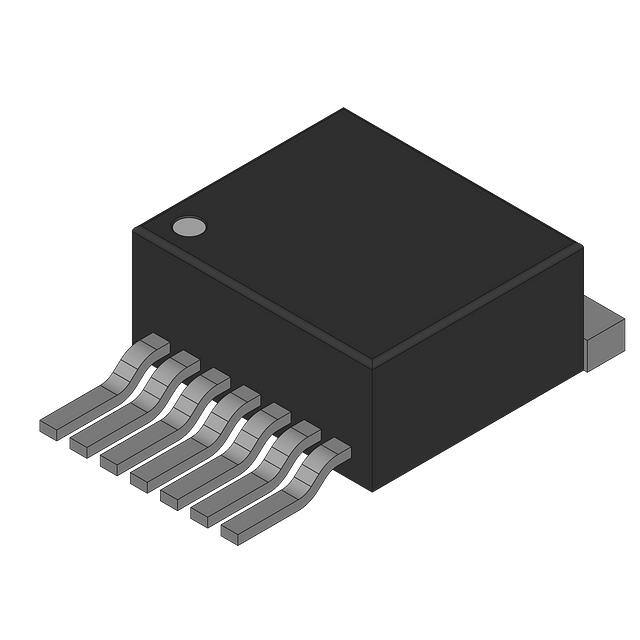
PG-TO263-7
Rev. 1.0, 2015-12-01
�TLS850D0TA
Overview
Functional Description
The TLS850D0TA is a high performance very low dropout linear voltage regulator for 5 V (TLS850D0V50) or 3.3 V
(TLS850D0V33) supply in a PG-TO263-7 package.
With an input voltage range of 3 V to 40 V and very low quiescent of only 40 µA, these regulators are perfectly
suitable for automotive or any other supply systems connected to the battery permanently. The TLS850D0TA
provides an output voltage accuracy of 2 % and a maximum output current up to 500 mA.
The new loop concept combines fast regulation and very good stability while requiring only one small ceramic
capacitor of 1 µF at the output. At currents below 100 mA the device will have a very low typical dropout voltage
of only 70 mV (for 5 V device) and 80 mV (for 3.3 V device). The operating range starts already at input voltages
of only 3 V (extended operating range). This makes the TLS850D0TA also suitable to supply automotive systems
that need to operate during cranking condition.
The device can be switched on and off by the Enable feature as described in Chapter 5.5.
The output voltage is supervised by the Reset feature, including Undervoltage Reset, delayed Reset at Power-On
and an adjustable lower Reset Threshold, more details can be found in Chapter 5.7.
Internal protection features like output current limitation and overtemperature shutdown are implemented to
protect the device against immediate damage due to failures like output short circuit to GND, over-current and
over-temperatures.
Choosing External Components
An input capacitor CI is recommended to compensate line influences. The output capacitor CQ is necessary for
the stability of the regulating circuit. TLS850D0TA is designed to be also stable with low ESR ceramic capacitors.
Type
Package
Marking
TLS850D0TAV50
PG-TO263-7
850D0V50
TLS850D0TAV33
PG-TO263-7
850D0V33
Data Sheet
4
Rev. 1.0, 2015-12-01
�TLS850D0TA
Block Diagram
2
Block Diagram
I
Q
Current
Limitation
Reset
EN
RO
RADJ
Enable
Bandgap
Reference
Temperature
Shutdown
DT
GND
Figure 2
Data Sheet
Block Diagram TLS850D0TAV50 and TLS850D0TAV33
5
Rev. 1.0, 2015-12-01
�TLS850D0TA
Pin Configuration
3
Pin Configuration
3.1
Pin Assignment TLS850D0TAV50 and TLS850D0TAV33
1 2 3 45 6 7
Q
DT
RADJ
GND
RO
EN
I
Figure 3
Pin Configuration
3.2
Pin Definitions and Functions TLS850D0TAV50 and TLS850D0TAV33
Pin
Symbol
Function
1
I
Input
It is recommended to place a small ceramic capacitor (e.g. 100 nF) to GND, close
to the IC terminals, in order to compensate line influences. See also Chapter 6.2.1
2
EN
Enable (integrated pull-down resistor)
Enable the IC with high level input signal;
Disable the IC with low level input signal;
3
RO
Reset Output (intergrated pull-up resistor to Q)
Open collector output;
Leave open if the reset function is not needed
4
GND
Ground
5
RADJ
Reset Threshold Adjustment
Connect to GND to use standard value;
Connect an external voltage divider to adjust reset threshold
6
DT
Delay Timing (integrated pull-down resistor)
Connect to GND or Q to select Reset timing acc. to Table 8
7
Q
Output Voltage
Connect output capacitor CQ to GND close to the IC’s terminals, respecting the
values specified for its capacitance and ESR in “Functional Range” on Page 8
Heat
Slug
–
Heat Slug
Connect to heatsink area;
Connect to GND
Data Sheet
6
Rev. 1.0, 2015-12-01
�TLS850D0TA
General Product Characteristics
4
General Product Characteristics
4.1
Absolute Maximum Ratings
Table 1
Absolute Maximum Ratings1)
Tj = -40 °C to +150 °C; all voltages with respect to ground (unless otherwise specified)
Parameter
Symbol
Values
Min.
Typ.
Max.
Unit Note /
Number
Test Condition
VI, VEN
-0.3
–
45
V
–
P_4.1.1
VQ, VRO
-0.3
–
7
V
–
P_4.1.3
Input I, Enable EN
Voltage
Output Q, Reset Output RO
Voltage
Delay Timing DT, Reset Threshold Adjustment RADJ
Voltage
VDT, VRADJ
-0.3
–
7
V
–
P_4.1.6
Tj
Tstg
-40
–
150
°C
–
P_4.1.7
-55
–
150
°C
–
P_4.1.8
-2
–
2
kV
2)
HBM
CDM
P_4.1.10
CDM
P_4.1.12
Temperatures
Junction Temperature
Storage Temperature
ESD Absorption
VESD
ESD Susceptibility to GND
VESD
ESD Susceptibility Pin 1, 7 (corner pins) VESD1,7
ESD Susceptibility to GND
-500
–
500
V
3)
-750
–
750
V
3)
P_4.1.9
to GND
1) Not subject to production test, specified by design.
2) ESD susceptibility, HBM according to ANSI/ESDA/JEDEC JS001 (1.5 kΩ, 100 pF)
3) ESD susceptibility, Charged Device Model “CDM” according JEDEC JESD22-C101
Note:
1. Stresses above the ones listed here may cause permanent damage to the device. Exposure to absolute
maximum rating conditions for extended periods may affect device reliability.
2. Integrated protection functions are designed to prevent IC destruction under fault conditions described in the
data sheet. Fault conditions are considered as “outside” normal operating range. Protection functions are not
designed for continuous repetitive operation.
Data Sheet
7
Rev. 1.0, 2015-12-01
�TLS850D0TA
General Product Characteristics
4.2
Functional Range
Table 2
Functional Range
Tj = -40 °C to +150 °C; all voltages with respect to ground (unless otherwise specified)
Parameter
Symbol
Input Voltage Range
VI
VI,ext
VEN
CQ
Values
Min.
Extended Input Voltage Range
Enable Voltage Range
Output Capacitor’s
Requirements for Stability
ESR
Junction Temperature
1)
2)
3)
4)
Typ.
VQ,nom + Vdr –
Unit
Note /
Test Condition
Number
V
1)
–
P_4.2.1
–
P_4.2.3
Max.
40
3.0
–
40
V
2)
0
–
40
V
–
1
ESR(CQ) –
Tj
-40
P_4.2.5
–
–
µF
3)4)
–
100
Ω
3)
–
150
°C
–
–
–
P_4.2.6
P_4.2.7
P_4.2.9
Output current is limited internaly and depends on the input voltage, see Electrical Characteristics for more details.
When VI is between VI,ext,min and VQ,nom + Vdr, VQ = VI - Vdr. When VI is below VI,ext,min, VQ can drop down to 0 V.
Not subject to production test, specified by design.
The minimum output capacitance requirement is applicable for a worst case capacitance tolerance of 30%
Note: Within the functional or operating range, the IC operates as described in the circuit description. The electrical
characteristics are specified within the conditions given in the Electrical Characteristics table.
Data Sheet
8
Rev. 1.0, 2015-12-01
�TLS850D0TA
General Product Characteristics
4.3
Thermal Resistance
Note: This thermal data was generated in accordance with JEDEC JESD51 standards. For more information, go
to www.jedec.org.
Table 3
Thermal Resistance
Parameter
Symbol
Values
Unit
Note /
Test Condition
Number
P_4.3.6
Min.
Typ.
Max.
–
3
–
K/W
1)
–
21
–
K/W
1)2)
Junction to Ambient
RthJC
RthJA
RthJA
–
75
–
Junction to Ambient
RthJA
–
42
Junction to Ambient
RthJA
–
34
Package Version PG-TO263-7
Junction to Case
Junction to Ambient
–
2s2p board
P_4.3.7
K/W
1)3)
1s0p board,
footprint only
P_4.3.8
–
K/W
1)3)
1s0p board,
300 mm2 heatsink
area on PCB
P_4.3.9
–
K/W
1)3)
P_4.3.10
1s0p board,
600 mm2 heatsink
area on PCB
1) Not subject to production test, specified by design
2) Specified RthJA value is according to Jedec JESD51-2,-5,-7 at natural convection on FR4 2s2p board; The Product
(Chip+Package) was simulated on a 76.2 x 114.3 x 1.5 mm³ board with 2 inner copper layers (2 x 70µm Cu, 2 x 35µm Cu).
Where applicable a thermal via array under the exposed pad contacted the first inner copper layer.
3) Specified RthJA value is according to JEDEC JESD 51-3 at natural convection on FR4 1s0p board; The Product
(Chip+Package) was simulated on a 76.2 × 114.3 × 1.5 mm3 board with 1 copper layer (1 x 70µm Cu).
Data Sheet
9
Rev. 1.0, 2015-12-01
�TLS850D0TA
Block Description and Electrical Characteristics
5
Block Description and Electrical Characteristics
5.1
Voltage Regulation
The output voltage VQ is divided by a resistor network. This fractional voltage is compared to an internal voltage
reference and the pass transistor is driven accordingly.
The control loop stability depends on the output capacitor CQ, the load current, the chip temperature and the
internal circuit design. To ensure stable operation, the output capacitor’s capacitance and its equivalent series
resistor (ESR) requirements given in “Functional Range” on Page 8 have to be maintained. For details, also see
the typical performance graph “Output Capacitor Series Resistor ESR(CQ) versus Output Current IQ” on
Page 15. As the output capacitor also has to buffer load steps, it should be sized according to the application’s
needs.
An input capacitor CI is recommended to compensate line influences. In order to block influences like pulses and
HF distortion at input side, an additional reverse polarity protection diode and a combination of several capacitors
for filtering should be used. Connect the capacitors close to the component’s terminals.
In order to prevent overshoots during start-up, a smooth ramp up function is implemented. This ensures almost
no output voltage overshoots during start-up, mostly independent from load and output capacitance.
Whenever the load current exceeds the specified limit, e.g. in case of a short circuit, the output current is limited
and the output voltage decreases.
The overtemperature shutdown circuit prevents the IC from immediate destruction under fault conditions (e.g.
output continuously short-circuit) by switching off the power stage. After the chip has cooled down, the regulator
restarts. This leads to an oscillatory behavior of the output voltage until the fault is removed. However, junction
temperatures above 150 °C are outside the maximum ratings and therefore significantly reduce the IC’s lifetime.
Supply
II
I
Q
Current
Limitation
Reset
EN
CI
RO
RADJ
Enable
VI
Bandgap
Reference
Temperature
Shutdown
Regulated
Output Voltage
IQ
C
VQ
ESR
DT
LOAD
CQ
GND
Figure 4
Voltage Regulation
V
VQ,nom
VI,ext,min
VI
Vdr
VQ
t
Figure 5
Data Sheet
Output Voltage vs. Input Voltage
10
Rev. 1.0, 2015-12-01
�TLS850D0TA
Block Description and Electrical Characteristics
Table 4
Electrical Characteristics Voltage Regulator 5 V version
Tj = -40 °C to +150 °C, VI = 13.5 V, all voltages with respect to ground (unless otherwise specified)
Typical values are given at Tj = 25 °C
Parameter
Symbol
Unit
Note / Test Condition
Number
Min.
Typ.
Max.
Output Voltage Precision
VQ
4.9
5.0
5.1
V
0.05 mA < IQ < 500 mA
5.95 V < VI < 28 V
P_5.1.3
Output Voltage Precision
VQ
4.9
5.0
5.1
V
0.05 mA < IQ < 200 mA
5.44 V < VI < 40 V
P_5.1.4
Output Voltage Start-up
slew rate
dVQ/dt
3.0
7.5
18
V/ms VI > 18 V/ms
CQ = 1 µF
0.5 V < VQ < 4.5 V
Output Current Limitation
IQ,max
501
∆VQ,load -20
650
1100 mA
0 V < VQ < 4.8 V
P_5.1.9
-1.5
5
mV
P_5.1.11
Line Regulation
steady-state
∆VQ,line
-20
0
20
mV
P_5.1.13
Dropout Voltage
Vdr = VI - VQ
Vdr
–
175
425
mV
IQ = 0.05 mA to 500 mA
VI = 6 V
VI = 8 V to 32 V
IQ = 5 mA
1)
IQ = 250 mA
Dropout Voltage
Vdr = VI - VQ
Vdr
–
70
170
mV
1)
IQ = 100 mA
P_5.1.17
Power Supply Ripple Rejection
PSRR
–
59
–
dB
2)
fripple = 100 Hz
P_5.1.18
Load Regulation
steady-state
Values
Overtemperature Shutdown
Threshold
Tj,sd
151
–
200
°C
Overtemperature Shutdown
Threshold Hysteresis
Tj,sdh
–
15
–
K
Vripple = 0.5 Vpp
2)
Tj increasing
2)
P_5.1.7
P_5.1.16
P_5.1.19
Tj decreasing
P_5.1.20
1) Measured when the output voltage VQ has dropped 100 mV from the nominal value obtained at VI = 13.5V
2) Not subject to production test, specified by design
Data Sheet
11
Rev. 1.0, 2015-12-01
�TLS850D0TA
Block Description and Electrical Characteristics
Table 5
Electrical Characteristics Voltage Regulator 3.3 V version
Tj = -40 °C to +150 °C, VI = 13.5 V, all voltages with respect to ground (unless otherwise specified)
Typical values are given at Tj = 25 °C
Parameter
Symbol
Unit
Note / Test Condition
Number
Min.
Typ.
Max.
Output Voltage Precision
VQ
3.23
3.3
3.37
V
0.05 mA < IQ < 500 mA
4.23 V < VI < 28 V
P_5.1.23
Output Voltage Precision
VQ
3.23
3.3
3.37
V
0.05 mA < IQ < 200 mA
3.72 V < VI < 40 V
P_5.1.24
Output Voltage Start-up
slew rate
dVQ/dt
3.0
7.5
18
V/ms VI > 18 V/ms
CQ = 1 µF
0.33 V < VQ < 2.97 V
Output Current Limitation
IQ,max
501
∆VQ,load -20
650
1100 mA
0 V < VQ < 3.1 V
P_5.1.29
-1.5
5
mV
P_5.1.31
Line Regulation
steady-state
∆VQ,line
-15
0
15
mV
Dropout Voltage
Vdr = VI - VQ
Vdr
–
200
430
mV
IQ = 0.05 mA to 500 mA
VI = 6 V
VI = 8 V to 32 V
IQ = 5 mA
1)
IQ = 250 mA
Dropout Voltage
Vdr = VI - VQ
Vdr
–
80
175
mV
1)
IQ = 100 mA
P_5.1.37
Power Supply Ripple Rejection
PSRR
–
63
–
dB
2)
fripple = 100 Hz
P_5.1.38
Load Regulation
steady-state
Values
Overtemperature Shutdown
Threshold
Tj,sd
151
–
200
°C
Overtemperature Shutdown
Threshold Hysteresis
Tj,sdh
–
15
–
K
Vripple = 0.5 Vpp
2)
Tj increasing
2)
P_5.1.27
P_5.1.33
P_5.1.36
P_5.1.39
Tj decreasing
P_5.1.40
1) Measured when the output voltage VQ has dropped 100 mV from the nominal value obtained at VI = 13.5V
2) Not subject to production test, specified by design
Data Sheet
12
Rev. 1.0, 2015-12-01
�TLS850D0TA
Block Description and Electrical Characteristics
5.2
Typical Performance Characteristics Voltage Regulator
Typical Performance Characteristics
Output Voltage VQ versus
Junction Temperature Tj (3.3 V version)
Output Voltage VQ versus
Junction Temperature Tj (5 V version)
3.5
IQ = 100mA
3.45
5.15
3.4
5.1
3.35
5.05
VQ [V]
VQ [V]
IQ = 100mA
3.3
5
3.25
4.95
3.2
4.9
3.15
4.85
3.1
0
50
Tj [°C]
100
4.8
150
Dropout Voltage Vdr versus
Junction Temperature Tj (3.3 V version)
0
100
150
Dropout Voltage Vdr versus
Junction Temperature Tj (5 V version)
350
350
IQ = 100 mA
IQ = 100 mA
300
50
Tj [°C]
IQ = 250 mA
300
IQ = 250 mA
250
250
200
200
Vdr [mV]
Vdr [mV]
VQ = 3.3 V
150
150
100
100
50
50
0
−40
Data Sheet
0
50
Tj [°C]
100
0
−40
150
13
0
50
Tj [°C]
100
150
Rev. 1.0, 2015-12-01
�TLS850D0TA
Block Description and Electrical Characteristics
Load Regulation ∆VQ,load versus
Output Current Change IQ
Line Regulation ∆VQ,line versus
Input Voltage VI
8
0
Tj = −40 oC
IQ = 5 mA
−2
Tj = 25 oC
6
Tj = 150 oC
−4
4
2
−8
ΔVQ,line [mV]
ΔVQ,load [mV]
−6
−10
−12
0
−2
−14
VI = 6 V
−16
−4
o
Tj = −40 C
Tj = 25 oC
−18
−6
o
Tj = 150 C
−20
0
100
200
300
IQ [mA]
400
−8
500
Output Voltage VQ versus
Input Voltage VI (3.3 V version)
10
15
20
VI [V]
25
30
Output Voltage VQ versus
Input Voltage VI (5 V version)
4
6
Tj = −40 °C
Tj = −40 °C
Tj = 25 °C
3.5
Tj = 25 °C
Tj = 150 °C
Tj = 150 °C
5
IQ = 100 mA
3
IQ = 100 mA
4
VQ [V]
VQ [V]
2.5
2
3
1.5
2
1
1
0.5
0
0
Data Sheet
1
2
3
VI [V]
4
5
0
6
14
0
1
2
3
VI [V]
4
5
6
Rev. 1.0, 2015-12-01
�TLS850D0TA
Block Description and Electrical Characteristics
Power Supply Ripple Rejection PSRR versus
ripple frequency f
Output Capacitor Series Resistor ESR(CQ) versus
Output Current IQ
3
80
10
VQ = 3.3 V
VQ = 5 V
70
Unstable Region
2
10
60
1
ESR(CQ) [Ω]
PSRR [dB]
50
40
30
10
Stable Region
0
10
20
−1
IQ = 10 mA
CQ = 1 μF
Vripple = 0.5 Vpp
Tj = 25 oC
10
0
−2
10
10
CQ = 1 μF
Tj = 25 oC
−2
−1
10
0
1
10
10
2
10
10
3
10
0.05
1
10
IQ [mA]
f [kHz]
Maximum Output Current IQ versus
Input Voltage VI
100
500
Dropout Voltage Vdr versus
Output Current IQ
1200
500
VQ = 3.3 V
450
VQ = 5 V
1000
Tj = 25 oC
400
350
300
Vdr [mV]
IQ,max [mA]
800
600
250
200
400
150
VQ = 0 V
100
Tj = −40 oC
200
Tj = 25 oC
50
Tj = 150 oC
0
0
Data Sheet
10
20
VI [V]
30
0
40
15
0
100
200
300
IQ [mA]
400
500
Rev. 1.0, 2015-12-01
�TLS850D0TA
Block Description and Electrical Characteristics
5.3
Current Consumption
Table 6
Electrical Characteristics Current Consumption
Tj = -40 °C to +150 °C, VI = 13.5 V (unless otherwise specified)
Typical values are given at Tj = 25 °C
Conditions of other pins: DT = GND
Parameter
Symbol
Values
Min.
Typ. Max.
Unit
Note / Test Condition
Number
Current Consumption
Iq = II
Iq,off
–
1.3
5
µA
VEN = 0 V; Tj < 105 °C
P_5.3.1
Current Consumption
Iq,off
–
–
8
µA
VEN = 0.4 V; Tj < 125 °C
P_5.3.3
Iq
–
40
52
µA
P_5.3.4
Current Consumption
Iq = II - IQ
Iq
–
62
77
µA
Current Consumption
Iq = II - IQ
Iq
–
62
82
µA
IQ = 0.05 mA
Tj = 25 °C
IQ = 0.05 mA
Tj < 125 °C
1)
IQ = 500 mA
Tj < 125 °C
Iq = II
Current Consumption
Iq = II - IQ
P_5.3.7
P_5.3.11
1) Not subject to production test, specified by design
Data Sheet
16
Rev. 1.0, 2015-12-01
�TLS850D0TA
Block Description and Electrical Characteristics
5.4
Typical Performance Characteristics Current Consumption
Typical Performance Characteristics
Current Consumption Iq versus
Output Current IQ
Current Consumption Iq versus
Input Voltage VI
200
100
Tj = −40 °C
Tj = 25 oC
90
180
70
140
60
120
Iq [uA]
Iq [μA]
Tj = 150 °C
160
80
50
80
30
60
20
40
10
20
0
Data Sheet
100
200
300
IQ [mA]
400
0
500
17
VEN = 5 V
IQ = 50 uA
100
40
0
Tj = 25 °C
5
10
15
20
25
VI [V]
30
35
40
Rev. 1.0, 2015-12-01
�TLS850D0TA
Block Description and Electrical Characteristics
5.5
Enable
The TLS850D0TA can be switched on and off by the Enable feature: Connect a HIGH level as specified below
(e.g. the battery voltage) to pin EN to enable the device; connect a LOW level as specified below (e.g. GND) to
shut it down. The enable has a built in hysteresis to avoid toggling between ON/OFF state, if signals with slow
slopes are applied to the EN input.
Table 7
Electrical Characteristics Enable
Tj = -40 °C to +150 °C, VI = 13.5 V, all voltages with respect to ground (unless otherwise specified)
Typical values are given at Tj = 25 °C
Parameter
Symbol
VEN,H
Low Level Input Voltage
VEN,L
Enable Threshold Hysteresis
VEN,Hy
High Level Input Current
IEN,H
High Level Input Current
IEN,H
Enable internal pull-down resistor REN
High Level Input Voltage
Data Sheet
Values
Unit
Note / Test Condition
Number
P_5.5.1
Min.
Typ.
Max.
2
–
–
V
–
–
0.8
V
VQ settled
VQ ≤ 0.1 V
100
–
–
mV
–
P_5.5.3
–
–
3.5
µA
P_5.5.4
–
–
22
µA
VEN = 3.3 V
VEN ≤ 18 V
0.95
1.5
2.6
MΩ
–
P_5.5.7
18
P_5.5.2
P_5.5.6
Rev. 1.0, 2015-12-01
�TLS850D0TA
Block Description and Electrical Characteristics
5.6
Typical Performance Characteristics Enable
Typical Performance Characteristics
Input Current IIN versus
Input Voltage VIN (condition: VEN = 0 V)
Enabled Input Current IEN versus
Enabled Input Voltage VEN
50
30
Tj = −40 °C
Tj = 25 °C
25
Tj = −40 °C
45
Tj = 150 °C
Tj = 25 °C
Tj = 150 °C
40
VEN = 0V
35
20
IEN [uA]
IIN [uA]
30
15
25
20
10
15
10
5
5
0
0
10
20
VIN [V]
30
Output Voltage VQ versus
time (EN switched ON, 5 V version)
0
6
6
5
5
4
4
3
2
10
20
VEN [V]
IQ = 100 mA
Tj = −40 °C
Tj = −40 °C
Tj = 25 °C
Tj = 25 °C
1
Tj = 150 °C
Tj = 150 °C
VEN
0
0
Data Sheet
500
1000
t [us]
1500
40
3
2
IQ = 100 mA
1
30
Output Voltage VQ versus
time (EN switched ON, 3.3 V version)
VQ, VEN [V]
VQ, VEN [V]
0
40
VEN
0
2000
19
0
500
1000
t [us]
1500
2000
Rev. 1.0, 2015-12-01
�TLS850D0TA
Block Description and Electrical Characteristics
5.7
Reset
The TLS850D0TA’s output voltage is supervised by the Reset feature, including Undervoltage Reset, delayed
Reset at Power-On and an adjustable Reset Threshold.
The Undervoltage Reset function sets the pin RO to LOW, in case VQ is falling for any reason below the Reset
Threshold VRT,low.
When the regulator is powered on, the pin RO is held at LOW for the duration of the Power-On Reset Delay Time
trd.
I
Q
RRO,int
Control
OR
R
CQ
RO
S
Reference
VDD
optional
Supply
Reset
IRO
Q
RADJ,1
OR
MicroController
RADJ
IRADJ
GND
BlockDiagram_ResetAdjust_TLS850D0.vs
d
optional
Timer
DT
RADJ,2
Figure 6
GND
Block Diagram Reset Circuit
Reset Delay Time
The pin DT is used to set the desired Reset Delay Time trd. Connect this pin either to GND or Q to select the timing
according to Table 8.
Table 8
Reset DelayTime Selection
DT connected to
trd
GND
16.5 ms
Q
8.5 ms
Power-On Reset Delay Time
The power-on reset delay time is defined by the parameter trd and allows a microcontroller and oscillator to start
up. This delay time is the time period from exceeding the upper reset switching threshold VRT,high until the reset is
released by switching the reset output “RO” from “LOW” to “HIGH”.
Undervoltage Reset Delay Time
Unlike the power-on reset delay time, the undervoltage reset delay time is defined by the parameter trd and
considers an output undervoltage event where the output voltage VQ trigger the VRT,low threshold.
Reset Blanking Time
The reset blanking time trr,blank avoids that short undervoltage spikes trigger an unwanted reset “low” signal.
Data Sheet
20
Rev. 1.0, 2015-12-01
�TLS850D0TA
Block Description and Electrical Characteristics
Reset Reaction Time
In case the output voltage of the regulator drops below the output undervoltage lower reset threshold VRT,low, the
reset output “RO” is set to low, after the delay of the internal reset reaction time trr,int. The reset blanking time trr,blank
is part of the reset reaction time trr,int.
Reset Output “RO”
The reset output “RO” is an open collector output with an integrated pull-up resistor. In case a lower-ohmic “RO”
signal is desired, an external pull-up resistor can be connected to the output “Q”. Since the maximum “RO” sink
current is limited, the minimum value of the optional external resistor “RRO,ext” is given in Table “Reset Output
RO” on Page 23.
Reset Output “RO” Low for VQ ≥ 1 V
In case of an undervoltage reset condition reset output “RO” is held “low” for VQ ≥ 1 V, even if the input voltage VI
is 0 V. This is achieved by supplying the reset circuit from the output capacitor.
Reset Adjust Function
The undervoltage reset switching threshold can be adjusted according to the application’s needs by connecting
an external voltage divider (RADJ1, RADJ2) at pin “RADJ”. For selecting the default threshold connect pin “RADJ” to
GND. The reset adjustment range for the TLS850D0TAV50 is given in Reset Threshold Adjustment Range. The
reset adjustment range for the TLS850D0TAV33 is given in Reset Threshold Adjustment Range.
When dimensioning the voltage divider, take into consideration that there will be an additional current constantly
flowing through the resistors.
With a voltage divider connected, the reset switching threshold VRT,new is calculated as follows
(neglecting the Reset Adjust Pin Current IRADJ):
VRT,lo,new = VRADJ,th × (RADJ,1 + RADJ,2) / RADJ,2
(1)
with
•
•
•
VRT,lo,new: Desired undervoltage reset switching threshold.
RADJ,1, RADJ,2: Resistors of the external voltage divider, see Figure 6.
VRADJ,th: Reset adjust switching threshold given in Reset Adjustment Switching Threshold.
Data Sheet
21
Rev. 1.0, 2015-12-01
�TLS850D0TA
Block Description and Electrical Characteristics
VI
t
VQ
t < trr,blank
VRH
VRT,hi gh
VRT,low
1V
t
trd
trr,int
trd
trr,int
trd
trr,int
VRO
trd
VRO,low
1V
t
Thermal
Shutdown
Figure 7
Data Sheet
Input
Voltage Dip
Undervoltage
Spike at
output
Over load
Typical Timing Diagram Reset
22
Rev. 1.0, 2015-12-01
�TLS850D0TA
Block Description and Electrical Characteristics
Table 9
Electrical Characteristics Reset
Tj = -40 °C to +150 °C, VI = 13.5 V, all voltages with respect to ground (unless otherwise specified)
Typical values are given at Tj = 25 °C
Parameter
Symbol
Values
Unit Note / Test Condition
Min.
Typ. Max.
Number
Output Undervoltage Reset 5V Version only
Output Undervoltage Reset Upper
Switching Threshold
VRT,high
4.6
4.7
4.8
V
VQ increasing
P_5.7.1
Output Undervoltage Reset Lower
Switching Threshold - Default
VRT,low
4.5
4.6
4.7
V
VQ decreasing
P_5.7.2
Output Undervoltage Reset
Switching Hysteresis
VRT,hy
60
100
–
mV
RADJ connected to GND P_5.7.3
Output Undervoltage Reset
Headroom VQ - VRT
VRH
200
400
–
mV
RADJ = GND
P_5.7.4
RADJ = GND
Output Undervoltage Reset 3V3 Version only
Output Undervoltage Reset Upper
Switching Threshold
VRT,high
3.08
3.15
3.22
V
VQ increasing
P_5.7.5
Output Undervoltage Reset Lower
Switching Threshold - Default
VRT,low
3.0
3.05
3.13
V
VQ decreasing
P_5.7.6
Output Undervoltage Reset
Switching Hysteresis
VRT,hy
60
100
–
mV
RADJ connected to GND P_5.7.7
Output Undervoltage Reset
Headroom VQ - VRT
VRH
100
250
–
mV
RADJ = GND
P_5.7.8
VRADJ,th
1.15
1.20
1.25
V
–
P_5.7.9
Reset Threshold Adjustment Range VRT,range
2.5
–
4.4
V
for VQ,nom = 5 V
P_5.7.10
Reset Threshold Adjustment Range VRT,range
2.5
–
2.9
V
for VQ,nom = 3.3 V
P_5.7.11
P_5.7.40
RADJ = GND
Reset Threshold Adjustment
Reset Adjustment Switching
Threshold
Reset Output RO
Reset Output Low Voltage
VRO,low
–
0.2
0.4
V
1 V ≤ VQ ≤ VRT;
RRO ≥ 5.1 kΩ
Reset Output
Internal Pull-Up Resistor
RRO,int
13
20
36
kΩ
internally connected to Q P_5.7.41
Reset Output External
Pull-up Resistor to VQ
RRO,ext
5.1
–
–
kΩ
1 V ≤ VQ ≤ VRT ;
VRO ≤ 0.4 V
P_5.7.42
trd,slow
trd,fast
13.2
16.5
19.8
ms
DT connected to GND
P_5.7.37
6.8
8.5
10.2
ms
DT connected to Q
P_5.7.38
µs
1)
for VQ,nom = 3.3 V
P_5.7.22
Reset Delay Timing
Reset Delay Time
Reset Delay Time
Reset blanking time
trr,blank
–
6
–
Reset blanking time
trr,blank
–
7
–
µs
2)
for VQ,nom = 5 V
P_5.7.46
Internal Reset Reaction Time
trr,int
trr,int
–
7
20
µs
for VQ,nom = 3.3 V
P_5.7.23
–
10
33
µs
for VQ,nom = 5 V
P_5.7.36
Internal Reset Reaction Time
Reset Delay Input DT
Data Sheet
23
Rev. 1.0, 2015-12-01
�TLS850D0TA
Block Description and Electrical Characteristics
Table 9
Electrical Characteristics Reset (cont’d)
Tj = -40 °C to +150 °C, VI = 13.5 V, all voltages with respect to ground (unless otherwise specified)
Typical values are given at Tj = 25 °C
Parameter
Symbol
Values
Min.
Unit Note / Test Condition
Number
P_5.7.29
Typ. Max.
Delay Input DT
High Signal Valid
VDT,H
2.0V –
–
V
Delay Input DT
Low Signal Valid
VDT,L
–
–
0.80
V
P_5.7.30
Delay Input DT
Signal Slew Rate
dVDT/dt
1
–
–
V/µs VDT,L < VDT < VDT,H
P_5.7.35
High Level Input Current
IDT,H
RDT
–
–
3.5
µA
VDT = 3.3 V
P_5.7.32
0.9
1.5
2.6
MΩ
Delay Input DT
internal pull-down resistor
–
P_5.7.33
1) Not subject to production test, specified by design.
2) Not subject to production test, specified by design.
Data Sheet
24
Rev. 1.0, 2015-12-01
�TLS850D0TA
Block Description and Electrical Characteristics
5.8
Typical Performance Characteristics Reset
Typical Performance Characteristics
Undervoltage Reset Threshold VRT versus
Junction Temperature Tj (5 V version)
3.5
5
3.4
4.9
3.3
4.8
3.2
4.7
3.1
4.6
VRT [V]
VRT [V]
Undervoltage Reset Threshold VRT versus
Junction Temperature Tj (3.3 V version)
3
2.9
4.5
4.4
2.8
4.3
IQ = 1 mA
VQ = 3.3 V
RADJ set to GND
2.7
VRT, high
2.6
IQ = 1 mA
VQ = 5 V
RADJ set to GND
4.2
VRT, high
4.1
VRT, low
2.5
0
50
Tj [°C]
100
VRT, low
4
150
Power On Reset Delay Time trd versus
Junction Temperature Tj
0
50
Tj [°C]
100
150
Internal Reset Reaction Time trr,int versus
Junction Temperature Tj
20
25
VQ = 3.3 V
fast
slow
IQ = 1 mA
18
VQ = 5 V
16
20
14
trr,int [us]
trd [ms]
12
15
10
8
6
10
4
2
5
Data Sheet
0
50
Tj [°C]
100
0
150
25
0
50
Tj [°C]
100
150
Rev. 1.0, 2015-12-01
�TLS850D0TA
Application Information
6
Application Information
6.1
Application Diagram
Note: The following information is given as a hint for the implementation of the device only and shall not be
regarded as a description or warranty of a certain functionality, condition or quality of the device.
Supply
I
Q
D I1
Current
Limitation
DI2
C I2
C I1


 工商网监
湘ICP备2023018690号
工商网监
湘ICP备2023018690号
