L o w P o w e r 3D Magnetic Sensor with I2C Interface
T L V 4 9 3 D - A 1 B 6 3D Magnetic Sensor
3D Magnetic Sensor
Data Sheet
Rev. 1.1, 2019-04-09
Sense & Control
�TLV493D-A1B6
3D Magnetic Sensor
Table of Contents
1
1.1
1.2
Product Description . . . . . . . . . . . . . . . . . . . . . . . . . . . . . . . . . . . . . . . . . . . . . . . . . . . . . . . . . . . . . . . . . . . . . . . 5
Target Applications . . . . . . . . . . . . . . . . . . . . . . . . . . . . . . . . . . . . . . . . . . . . . . . . . . . . . . . . . . . . . . . . . . . . . . . 5
Features . . . . . . . . . . . . . . . . . . . . . . . . . . . . . . . . . . . . . . . . . . . . . . . . . . . . . . . . . . . . . . . . . . . . . . . . . . . . . . . . . 5
2
2.1
2.1.1
2.1.2
2.2
2.3
2.4
2.5
Functional Description . . . . . . . . . . . . . . . . . . . . . . . . . . . . . . . . . . . . . . . . . . . . . . . . . . . . . . . . . . . . . . . . . . . . 6
General . . . . . . . . . . . . . . . . . . . . . . . . . . . . . . . . . . . . . . . . . . . . . . . . . . . . . . . . . . . . . . . . . . . . . . . . . . . . . . . . . . 6
Power Mode Control . . . . . . . . . . . . . . . . . . . . . . . . . . . . . . . . . . . . . . . . . . . . . . . . . . . . . . . . . . . . . . . . . . . . 6
Sensing Part . . . . . . . . . . . . . . . . . . . . . . . . . . . . . . . . . . . . . . . . . . . . . . . . . . . . . . . . . . . . . . . . . . . . . . . . . . . . 7
Pin Configuration (top view) . . . . . . . . . . . . . . . . . . . . . . . . . . . . . . . . . . . . . . . . . . . . . . . . . . . . . . . . . . . . . . . 8
Definition of Magnetic Field . . . . . . . . . . . . . . . . . . . . . . . . . . . . . . . . . . . . . . . . . . . . . . . . . . . . . . . . . . . . . . . . 8
Sensitive Area . . . . . . . . . . . . . . . . . . . . . . . . . . . . . . . . . . . . . . . . . . . . . . . . . . . . . . . . . . . . . . . . . . . . . . . . . . . . 9
Application Circuit . . . . . . . . . . . . . . . . . . . . . . . . . . . . . . . . . . . . . . . . . . . . . . . . . . . . . . . . . . . . . . . . . . . . . . . 10
3
3.1
3.2
3.3
3.4
Specification . . . . . . . . . . . . . . . . . . . . . . . . . . . . . . . . . . . . . . . . . . . . . . . . . . . . . . . . . . . . . . . . . . . . . . . . . . . . 11
Absolute Maximum Ratings . . . . . . . . . . . . . . . . . . . . . . . . . . . . . . . . . . . . . . . . . . . . . . . . . . . . . . . . . . . . . . . 11
Operating Range . . . . . . . . . . . . . . . . . . . . . . . . . . . . . . . . . . . . . . . . . . . . . . . . . . . . . . . . . . . . . . . . . . . . . . . . 11
Electrical Characteristics . . . . . . . . . . . . . . . . . . . . . . . . . . . . . . . . . . . . . . . . . . . . . . . . . . . . . . . . . . . . . . . . . 13
Temperature Measurement (default = activated) . . . . . . . . . . . . . . . . . . . . . . . . . . . . . . . . . . . . . . . . . . . 14
4
Interface and Timing Description . . . . . . . . . . . . . . . . . . . . . . . . . . . . . . . . . . . . . . . . . . . . . . . . . . . . . . . . . . 15
5
Magnetic Characteristics . . . . . . . . . . . . . . . . . . . . . . . . . . . . . . . . . . . . . . . . . . . . . . . . . . . . . . . . . . . . . . . . . 17
6
Characteristical . . . . . . . . . . . . . . . . . . . . . . . . . . . . . . . . . . . . . . . . . . . . . . . . . . . . . . . . . . . . . . . . . . . . . . . . . . 18
7
7.1
7.2
Package Information . . . . . . . . . . . . . . . . . . . . . . . . . . . . . . . . . . . . . . . . . . . . . . . . . . . . . . . . . . . . . . . . . . . . . 19
Package Parameters . . . . . . . . . . . . . . . . . . . . . . . . . . . . . . . . . . . . . . . . . . . . . . . . . . . . . . . . . . . . . . . . . . . . . 19
Package Outlines . . . . . . . . . . . . . . . . . . . . . . . . . . . . . . . . . . . . . . . . . . . . . . . . . . . . . . . . . . . . . . . . . . . . . . . . 19
8
Revision History . . . . . . . . . . . . . . . . . . . . . . . . . . . . . . . . . . . . . . . . . . . . . . . . . . . . . . . . . . . . . . . . . . . . . . . . . 22
Data Sheet
2
Rev. 1.1, 2019-04-09
�TLV493D-A1B6
3D Magnetic Sensor
List of Tables
Table 1
Table 2
Table 3
Table 4
Table 5
Table 6
Table 7
Table 8
Table 9
Table 10
Table 11
Table 12
Table 13
Data Sheet
Ordering Information . . . . . . . . . . . . . . . . . . . . . . . . . . . . . . . . . . . . . . . . . . . . . . . . . . . . . . . . . . . . . . . . . . 5
TSOP-6 Pin Description and Configuration (see Figure 1) . . . . . . . . . . . . . . . . . . . . . . . . . . . . . . . . . . . 8
Absolute Maximum Ratings . . . . . . . . . . . . . . . . . . . . . . . . . . . . . . . . . . . . . . . . . . . . . . . . . . . . . . . . . . . . 11
ESD Protection (Ta = 25°C) . . . . . . . . . . . . . . . . . . . . . . . . . . . . . . . . . . . . . . . . . . . . . . . . . . . . . . . . . . . . . 11
Operating Range . . . . . . . . . . . . . . . . . . . . . . . . . . . . . . . . . . . . . . . . . . . . . . . . . . . . . . . . . . . . . . . . . . . . . . 11
VDD power up and power-cycle. . . . . . . . . . . . . . . . . . . . . . . . . . . . . . . . . . . . . . . . . . . . . . . . . . . . . . . . . . 12
Electrical Setup . . . . . . . . . . . . . . . . . . . . . . . . . . . . . . . . . . . . . . . . . . . . . . . . . . . . . . . . . . . . . . . . . . . . . . . 13
Temperature Measurement Characteristics . . . . . . . . . . . . . . . . . . . . . . . . . . . . . . . . . . . . . . . . . . . . . 14
Interface and Timing . . . . . . . . . . . . . . . . . . . . . . . . . . . . . . . . . . . . . . . . . . . . . . . . . . . . . . . . . . . . . . . . . . 15
Conversion table for 12Bit . . . . . . . . . . . . . . . . . . . . . . . . . . . . . . . . . . . . . . . . . . . . . . . . . . . . . . . . . . . . . 16
Initial Magnetic Characteristics . . . . . . . . . . . . . . . . . . . . . . . . . . . . . . . . . . . . . . . . . . . . . . . . . . . . . . . . . 17
Sensor Drifts . . . . . . . . . . . . . . . . . . . . . . . . . . . . . . . . . . . . . . . . . . . . . . . . . . . . . . . . . . . . . . . . . . . . . . . . . . 17
Package Parameters . . . . . . . . . . . . . . . . . . . . . . . . . . . . . . . . . . . . . . . . . . . . . . . . . . . . . . . . . . . . . . . . . . 19
3
Rev. 1.1, 2019-04-09
�TLV493D-A1B6
3D Magnetic Sensor
List of Figures
Figure 1
Figure 2
Figure 3
Figure 4
Figure 5
Figure 6
Figure 7
Figure 8
Figure 9
Figure 10
Figure 11
Figure 12
Figure 13
Figure 14
Data Sheet
All three Sensitive Directions Bx, By and Bz . . . . . . . . . . . . . . . . . . . . . . . . . . . . . . . . . . . . . . . . . . . . . . . 5
Block Diagram . . . . . . . . . . . . . . . . . . . . . . . . . . . . . . . . . . . . . . . . . . . . . . . . . . . . . . . . . . . . . . . . . . . . . . . . . 6
Pinout . . . . . . . . . . . . . . . . . . . . . . . . . . . . . . . . . . . . . . . . . . . . . . . . . . . . . . . . . . . . . . . . . . . . . . . . . . . . . . . . 8
Definition of Magnetic Field Direction . . . . . . . . . . . . . . . . . . . . . . . . . . . . . . . . . . . . . . . . . . . . . . . . . . . . 8
Center of Sensitive Area. . . . . . . . . . . . . . . . . . . . . . . . . . . . . . . . . . . . . . . . . . . . . . . . . . . . . . . . . . . . . . . . . 9
Application Circuit with external Power Supply and µC . . . . . . . . . . . . . . . . . . . . . . . . . . . . . . . . . . . 10
VDD power up and power-cycle for high availability . . . . . . . . . . . . . . . . . . . . . . . . . . . . . . . . . . . . . . . 12
I2C Timing Specification. . . . . . . . . . . . . . . . . . . . . . . . . . . . . . . . . . . . . . . . . . . . . . . . . . . . . . . . . . . . . . . . 15
IDD versus Temperature . . . . . . . . . . . . . . . . . . . . . . . . . . . . . . . . . . . . . . . . . . . . . . . . . . . . . . . . . . . . . . . . 18
Image of TLV493D-A1B6 in PG-TSOP-6-6-5 . . . . . . . . . . . . . . . . . . . . . . . . . . . . . . . . . . . . . . . . . . . . . . . 19
Footprint PG-TSOP-6-6-5, Reflow Soldering (all dimensions in mm) . . . . . . . . . . . . . . . . . . . . . . . . 19
Footprint PG-TSOP-6-6-5, Wave Soldering (all dimensions in mm). . . . . . . . . . . . . . . . . . . . . . . . . . 20
Package Outlines (all dimensions in mm) . . . . . . . . . . . . . . . . . . . . . . . . . . . . . . . . . . . . . . . . . . . . . . . . 20
Packing (all dimensions in mm). . . . . . . . . . . . . . . . . . . . . . . . . . . . . . . . . . . . . . . . . . . . . . . . . . . . . . . . . 21
4
Rev. 1.1, 2019-04-09
�TLV493D-A1B6
3D Magnetic Sensor
Product Description
1
Product Description
1.1
Target Applications
The 3D magnetic sensor TLV493D-A1B6 offers accurate three-dimensional sensing with extremely low power
consumption in a small 6-pin package. With its magnetic field detection in x, y, and z-direction the sensor
reliably measures three-dimensional, linear and rotation movements. Applications include joysticks, control
elements (white goods, multifunction knops), or electric meters (anti tampering) and any other application
that requires accurate angular measurements or low power consumptions.
The integrated temperature sensor can furthermore be used for plausibility checks.
N
N
S
Z
X
D
GN D
T)
G N L (/ IN
C
S
D
VD
Y
D
GN
D
( AD
S
R)
DA
N
S
Figure 1
All three Sensitive Directions Bx, By and Bz
1.2
Features
S
•
3D magnetic sensing
•
Very low power consumption = 10 µA during operations (10 Hz, typ.)
•
Power down mode with 7 nA power consumption
•
Digital output via 2-wire based standard I2C interface up to 1 MBit/sec
•
12-bit data resolution for each measurement direction
•
Bx, By and Bz linear field measurement up to +130 mT
•
Excellent matching of X/Y measurement for accurate angle sensing
•
Variable update frequencies and power modes (configurable during operation)
•
Supply voltage range = 2.8 V…3.5 V, Temperature range Tj = -40°C…125°C
•
Small, industrial 6 pin TSOP package
•
Triggering by external µC possible
•
Interrupt signal available to wake up a microcontroller
•
Temperature measurement
Table 1
Ordering Information
Product Name
Marking
Ordering Code
Package
3D Magnetic Sensor
TLV493D-A1B6
VA (serie)
SP001286056
PG-TSOP-6-6-5
Data Sheet
5
Rev. 1.1, 2019-04-09
�TLV493D-A1B6
3D Magnetic Sensor
Functional Description
2
Functional Description
2.1
General
Description of the Block diagram and its functions.
F-OSC
Power Mode Control
LP-OSC
VDD
GND
Bias
Spinning
vertical-Hall plates
X-Direction
SCL; /INT
Spinning lat.
Hall plates
Z-Direction
Comparator
z
ADC
Digital tracking ,
demodulation &
I²C interface
SDA
MUX
Spinning
vertical -Hall plates
Y-Direction
Register & Interface
Sensing Part
Temperature
Figure 2
Block Diagram
The IC consists of three main function units containing the following building blocks:
•
The power mode control system, containing a low-power oscillator, basic biasing, accurate reset,
undervoltage detection and a fast oscillator.
•
The sensing part, containing the HALL biasing, HALL probes with multiplexers and successive tracking ADC.
Furthermore a temperature sensor is implemented.
•
The I2C interface, containing the register file and I/O pads.
2.1.1
Power Mode Control
The power mode control provides the power distribution in the IC, a power-on reset function and a specialized
low-power oscillator clock source. Additionally it is handling the start-up behavior.
•
On start-up this unit:
– activates the biasing, provides an accurate reset detector and fast oscillator.
– interprets the applied voltage level on ADDR pin as logical “0” or “1”. This determines one of two
possible I2C bus addresses to access the sensor.
– sensor enters power down mode (configured via I2C interface).
Note: After supplying the sensor (= power up) the sensor enters the mode power down by default.
Data Sheet
6
Rev. 1.1, 2019-04-09
�TLV493D-A1B6
3D Magnetic Sensor
Functional Description
•
After re-configuration to one of the operating modes a measurement cycle is performed regularly
containing of:
– starts the internal biasing, checks for reset condition and provides the fast oscillator
– provides the HALL biasing
– the measurement of the three HALL probe channels sequentially incl. temperature (default = activated)
– and enters the configured mode again
In any case functions are only executed if the supply voltage is high enough, otherwise the reset circuit will halt
the state machine until the level is reached and restarts its operation afterwards. The functions are also
restarted if a reset event occurs in between.
2.1.2
Sensing Part
Performs the measurements of the magnetic field in X, Y and Z direction. Each X, Y and Z-HALL probe is
connected sequentially to a multiplexer, which is then connected to an Analog to Digital Converter (ADC).
Optionally, the temperature is determined as well after the three HALL channels. The current consumption
decreases by -25 % when temperature measurement is deactivated.
Data Sheet
7
Rev. 1.1, 2019-04-09
�TLV493D-A1B6
3D Magnetic Sensor
Functional Description
2.2
Pin Configuration (top view)
Figure 3 shows the pinout of the TLV493D-A1B6.
6
5
4
1
2
3
Figure 3
Pinout
Table 2
TSOP-6 Pin Description and Configuration (see Figure 1)
Pin No.
Name
Description
1
SCL
/INT
Interface serial clock pin (input)
Interrupt pin, signals a finished measurement cycle
2
GND
connect to GND
3
GND
Ground Pin
4
VDD
Supply Pin
5
GND
connect to GND
6
SDA
ADDR
Interface serial data pin (input/output), open drain
Sensor ID configuration during power up
2.3
Definition of Magnetic Field
A positive field is considered as South-Pole facing the corresponding Hall element.
Figure 4 shows the definition of the magnetic directions X, Y, Z of the TLV493D-A1B6.
N
N
S
S
S
N
X-Axis
Figure 4
Data Sheet
Y-Axis
Z-Axis
Definition of Magnetic Field Direction
8
Rev. 1.1, 2019-04-09
�TLV493D-A1B6
3D Magnetic Sensor
Functional Description
2.4
Sensitive Area
1
Figure 5
Data Sheet
Center of Sensitive Area
9
Rev. 1.1, 2019-04-09
�TLV493D-A1B6
3D Magnetic Sensor
Functional Description
2.5
Application Circuit
The use of an interrupt line is optional, but highly recommended to ensure proper and efficient readout of the
sensor data.
The pull-up resistors R1 & R2 of the I2C bus have to be set in a way to keep the rise- and fall time specification
of the interface bus parameters (see specification section) with the parasitic capacitive load of the actual
setup.
The serial resistances R between SDA /SCL & Pull up R1/R2 may be used to avoid reflections on longer bus lines
causing ground bouncing on sensor side and communication issues.
The series resistance R between and the SCL µC pin and the pull up resistor R2 together with the capacitance
C2 to ground may provide additional EMC filtering if required.
Please note: too small resistive values for R1/2 have to be prevented to avoid unnecessary power consumption
during interface transmissions, especially for low-power applications. The additional capacitor C2 on the SCL
line will limit the maximum possible bitrate on the bus.
R1/2 = 1.2 kΩ
C1 = 100 nF
R = 100 Ω
C = 200 pF
VDD
Power
Supply
R1
VDD
SDA
R2
GND
R
µC
C1
TLV493D
e.g.
SCL
GND
Figure 6
(/INT)
R
R
CBuf
XMC 1100
C2
Application Circuit with external Power Supply and µC
For additional EMC precaution in harsh environments, C1 may be implemented by two 100 nF capacitors in
parallel, which should be already given by CBuf near the µC and/or power supply.
Data Sheet
10
Rev. 1.1, 2019-04-09
�TLV493D-A1B6
3D Magnetic Sensor
Specification
3
Specification
3.1
Absolute Maximum Ratings
Attention:
Stresses above those listed under “Absolute Maximum Ratings” may cause permanent damage to
the device. This is a stress rating only and functional operation of the device at these or any other
conditions above those indicated in the operational sections of this specification is not implied.
Furthermore, only single error cases are assumed. More than one stress/error case may also
damage the device.
Exposure to absolute maximum rating conditions for extended periods may affect device reliability.
During absolute maximum rating overload conditions the voltage on VDD pins with respect to ground
(VSS) must not exceed the values defined by the absolute maximum ratings.
Table 3
Absolute Maximum Ratings
Parameter
Symbol
min
typ
max
Unit
Junction temperature
Tj
-40
–
125
°C
Voltage on VDD
VDD
-0.3
–
3.5
V
Magnetic field
Bmax
–
–
1
T
Voltage range on any pin to
GND
Vmax
-0.1
–
3.5
V
Table 4
Note/Condition
open-drain outputs are not
current limited
ESD Protection1) (Ta = 25°C)
Parameter
Symbol
ESD voltage (HBM)2)
Values
VESD
3)
ESD voltage (CDM)
Unit
Note or Test Condition
Min.
Typ.
Max.
-1.5
–
1.5
kV
R = 1.5 kΩ, C = 100 pF
–
–
750
V
for corner pins
–
–
500
V
all pins
1) Characterization of ESD is carried out on a sample basis, not subject to production test.
2) Human Body Model (HBM) tests according to ANSI/ESDA/JEDEC JS-001.
3) Charged Device Model (CDM), ESD susceptibility according to JEDEC JESD22-C101.
3.2
Operating Range
Table 5
Operating Range
Parameter
Symbol
min
typ
max
Unit
Note/Condition
Operating temperature
Tj
-40
–
125
°C
Tj = Ta + 3°C as worst case assumption
Supply voltage
VDD
2.8
3.3
3.5
V
see Note below
Reset level
Vres
–
2.2
–
V
see Note below
Data Sheet
11
Rev. 1.1, 2019-04-09
�TLV493D-A1B6
3D Magnetic Sensor
Specification
To provide these ultra low power consumption figures, the chip does not use a classic (and current
consuming) reset concept. The implemented reset focus is on ensuring a proper supply for the ADC operation
only (so it inhibits the ADC reliably until the sensor supply is high enough). Thus, the sensor rely on a proper
supply ramp including IDD-PUP current consumption during power-on to ensure it is initialized correctly. The I2C
reset feature of the sensor shall be used by the µC after power-up. If supply monitoring is used in the system
(e.g. brown-out detector etc.) it is also recommended to use the I2C reset of the sensor upon events detected
by this monitor.
VDD
VOUS
3.3V
tPUP
t
Figure 7
VDD power up and power-cycle for high availability
Table 6
VDD power up and power-cycle
Parameter
Symbol
min
typ
max
Unit
Power Up ramp time
tPUP
–
–
10
µs
Power Up overundershoot
VOUS
3
3.3
3.5
V
Envelope which must not be
exceeded at the end of a Power Up.
Power Up current
consumption
IDD-PUP
–
3.7
–
mA
Current consumption during tPUP
Data Sheet
12
Note/Condition
Rev. 1.1, 2019-04-09
�TLV493D-A1B6
3D Magnetic Sensor
Specification
3.3
Electrical Characteristics
Note: All specification parameters refer to 3.3 V +5 % nominal supply VDD on the pins directly. Typical values
refer to 25°C and to 3.3 V +5 % nominal supply.
Table 7
Electrical Setup
Parameter
Supply current
1)
Symbol min
typ
max
Unit
Note/Condition
IDD
–
7
100
nA
power down mode (default
after power on), all off
–
10
–
µA
ultra low power mode
–
80
–
µA
low power mode
Average operating current
IDD_op
–
3.7
–
mA
peak during ADC measurements
for about 270 µs2) 3)
Input voltage low threshold
VIL
–
–
20
%VDD
all input pads
Input voltage high threshold
VIH
70
–
–
%VDD
all input pads
Input voltage hysteresis threshold VI_Hyst
5
–
–
%VDD
all input pads
Output voltage low level @ 3 mA
load
VOL
–
–
0.4
V
all output pads, static load
Fall time SDA/SCL signal 4)
tFALL
–
0.255) 0.3
µs
0.3 µs for 400 kHz mode (or may
require less C load)
Rise time SDA/SCL signal 4)
tRISE
–
0.55)
–
µs
R = 1.2 kΩ
Output high level
VOH
–
VDD
–
V
given by ext. pull-up resistor
1) Average values
2) During power down mode the current consumption is about 7 nA
3) Current at Pull ups needs to be considered for power supply dimensioning, consider minimum 10 mA for the power
supply for the sensor only
4) Dependent on used R-C-combination
5) For given AppCircuit; Capacitive load (parasitics and discrete caps used) for each bus line = 200 pF (SDA, SCL)
Note: The average supply current IDD in the low power modes and I2C triggered mode will decrease by about
25% when the temperature measurement is disabled.
Data Sheet
13
Rev. 1.1, 2019-04-09
�TLV493D-A1B6
3D Magnetic Sensor
Specification
3.4
Temperature Measurement (default = activated)
Table 8
Temperature Measurement Characteristics
Parameter
Symbol
min
typ
max
Unit
Digital value @ 25°C
T25
–
340
–
LSB
Resolution 12 bit
TRes12
–
1.1
–
°C/LSB
Accuracy
TACC
–
+10
–
°C
1)
Note/Condition
1) Theoretical possible measurement range from -50°C to 150°C
Data Sheet
14
Rev. 1.1, 2019-04-09
�TLV493D-A1B6
3D Magnetic Sensor
Interface and Timing Description
4
Interface and Timing Description
This chapter refers to how to set the boundary conditions in order to establish a proper interface
communication.
Table 9
Interface and Timing1)
Parameter
Symbol
min
typ
max
Unit
Note/Condition
Update rate X, Y, Z
fUr
–
3.3
–
kHz
max. ADC conversion rate
Update rate (all axis), ultra low p.
fUr_ulp
–
10
–
Hz
int. triggered
Update rate (all axis), low p.
fUr_lp
–
100
–
Hz
int. triggered
End-of-Conversion /INT pulse
tINT
–
1.5
–
µs
low-active (when activated)
Internal clock accuracy
tclk_E
-25
–
25
%
all above timing parameters
Allowed I2C bit clock frequency2)
fI2C_clk
–
400
1000
kHz
400 kHz is I2C fast mode
Low period of SCL clock
tL
0.5
–
–
µs
1.3 µs for 400 kHz mode
High period of SCL clock
tH
0.4
–
–
µs
0.6 µs for 400 kHz mode
SDA fall to SCL fall hold time
(hold time start condition to clock)
tSTA
0.4
–
–
µs
0.6 µs for 400 kHz mode
SCL rise to SDA rise su. time
tSTOP
(setup time clock to stop condition)
0.4
–
–
µs
0.6 µs for 400 kHz mode
SDA rise to SDA fall hold time
tWAIT
(wait time from stop to start cond.)
0.4
–
–
µs
0.6 µs for 400 kHz mode
SDA setup before SCL rising
tSU
0.1
–
–
µs
SDA hold after SCL falling
tHOLD
0
–
–
µs
1) Not subject to production test - verified by design/characterization
2) Dependent on R-C-combination on SDA and SCL. Ensure reduced capacitive load for speeds above 400 kHz.
tH
tL
tSTOP
tWAIT
tSTA
70% VDD
SCL
pin
20% VDD
70% VDD
SDA
pin
20% VDD
tHOLD
tSU
1 bit transfer
Figure 8
Data Sheet
STOP cond .
START cond .
I2C Timing Specification
15
Rev. 1.1, 2019-04-09
�TLV493D-A1B6
3D Magnetic Sensor
Interface and Timing Description
Managing correct sensor read outs by the µC:
This sensor does not incorporate shadow-buffers for readout. Thus, it is mandatory to read the sensor data
not during a running conversion to avoid corrupted reads. Ideally, the /INT feature is enabled together with
the low-power or ultra-low power mode and the µC reads the data after the /INT pulse was asserted by the
sensor. Furthermore, the readout needs to be finished before a new conversion is started and the /INT will be
asserted again (if the readout is finished 1 ms before a new /INT pulse, this will be sufficient).
Conversion register value to magnetic field and temperature value:
The conversion is realized by the two’s complement. Please use following table for transformation:
Table 10
e.g.
Conversion table for 12Bit
MSB
Bit11
Bit10
Bit9
Bit8
Bit7
Bit6
Bit5
Bit4
Bit3
Bit2
LSB
-2048
1024
512
256
128
64
32
16
8
4
2
1
1
1
1
1
0
0
0
0
1
1
1
1
Example for 12Bit read out: 1111 0000 1111: -2048 + 1024 + 512 + 256 + 0 + 0 + 0 + 0 + 8 + 4 + 2 +1 = -241 LSB
Calculation to mT: -241 LSB * 0.098 mT/LSB = -23.6 mT
For further information and a detailed I2C bitmap please refer to user manual.
Data Sheet
16
Rev. 1.1, 2019-04-09
�TLV493D-A1B6
3D Magnetic Sensor
Magnetic Characteristics
5
Magnetic Characteristics
Table 11
Initial Magnetic Characteristics1)
Values for 25°C, 0 h and VDD = 3.3 V
Parameter
Symbol
min
typ
max
Unit
Note/Condition
Usable magnetic linear range2)
Bxyz_LIN
–
+130
–
mT
Bx, By and Bz
Offset
BO
-1
+0.2
1
mT
Bx, By and Bz
Sensitivity
Sx, Sy, Sz –
10.2
–
LSB12/ Bx, By and Bz; (12bit)
mT
Resolution 12-bit readout3)
Res12
–
98
–
µT/
LSB12
Resolution 8-bit readout3)
Res8
–
1.56
–
mT/
LSB8
Magnetic noise (rms)
Bineff
–
0.1
–
mT
rms = 1 sigma
2)
BHYS
–
1
–
LSB12
due to quantization effects
Magnetic hysteresis
1) Magnetic test on wafer level. It is assumed that initial variations are stored and compensated in the external µC during
module test and calibration.
2) Not subject to production test - verified by design/characterization.
3) Resolution is calculated as 1/Sensitivity (and multiplied by 16 for 8-bit value)
Table 12
Sensor Drifts1)
Values for VDD = 3.3 V +5 %, Tj = -40 to 125°C, static magnetic field within usable linear range
Parameter
Symbol
Sensitivity drift
typ
max
Unit
Note/Condition
SxD, SyD, SzD –
+20
–
%
Bx, By and Bz
BO_D
-1
+0.2
1
mT
Bx, By and Bz; @ 0mT
MXY_D
–
+5
–
%
–
+20
–
%
TC
–
0
–
ppm/K Bx, By and Bz
DNL (Differential Non Linearity)
DNL
–
+5
–
LSB12
INL (Integral Non Linearity)1)
INL
–
0.1
–
%FSR4) Bx, By and Bz
Offset drift
2)
X to Y magnetic matching drift
X/Y to Z magnetic matching drift2) MX/YZ_D
Temperature compensation
3)
1)
min
Bx, By and Bz
1) Not subject to production test, verified by design/characterization. Drifts are changes from the initial characteristics
due to external influences.
2) See the magnetic matching definition in Equation (5.1) and Equation (5.2).
3) Can be changed by I2C command during operation; further typical values are -2000, -1000, 500 ppm/K
4) The FSR is calculated as ±2048 · Res12
Data Sheet
17
Rev. 1.1, 2019-04-09
�TLV493D-A1B6
3D Magnetic Sensor
Characteristical
Equation for parameter “X to Y magnetic matching”:
(5.1)
100 ∙ 2 ∙
%
Equation for parameter “X/Y to Z magnetic matching”:
/
6
(5.2)
100 ∙ 2 ∙
2 ∙
2 ∙
%
Characteristical
IDD vs Temperature
10.000,00
1.000,00
IDD [uA] - log scale
100,00
IC1: Power down
mode
10,00
IC1: Ultra low power
mode
IC1: Low power
mode
1,00
IC 1: Average ADC
Operating Current
0,10
IC2: Power down
mode
IC2: Ultra low power
mode
0,01
IC2: Low power
mode
0,00
-55
-35
-15
5
25
45
65
85
105
125
IC2: Average ADC
Operating Current
Temperature [°C]
Figure 9
Data Sheet
IDD versus Temperature
18
Rev. 1.1, 2019-04-09
�TLV493D-A1B6
3D Magnetic Sensor
Package Information
7
Package Information
7.1
Package Parameters
Table 13
Package Parameters
Parameter
Symbol Limit Values
Min.
Typ.
Max.
Unit
Notes
Thermal resistance
Junction ambient
RthJA
–
–
200
K/W
Junction to air1)
for PG-TSOP6-6-5
Thermal resistance
Junction lead
RthJL
–
–
100
K/W
Junction to lead
for PG-TSOP6-6-5
Soldering moisture level
MSL 1
260°C2)
1) according to Jedec JESD51-7
2) suitable for reflow soldering with soldering profiles according to JEDEC J-STD-020D.1 (March 2008)
7.2
Package Outlines
Figure 10
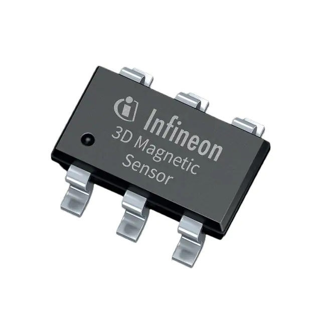
Image of TLV493D-A1B6 in PG-TSOP-6-6-5
2.9
1.9
0.5
0.95
Figure 11
Data Sheet
Footprint PG-TSOP-6-6-5, Reflow Soldering (all dimensions in mm)
19
Rev. 1.1, 2019-04-09
�TLV493D-A1B6
3D Magnetic Sensor
Package Information
4.3
1.9
0.55
0.95
Figure 12
R
k W Soldering
ld i(all dimensions
ibl d in mm)
Footprint PG-TSOP-6-6-5,
Wave
Figure 13
Package Outlines (all dimensions in mm)
Data Sheet
20
Rev. 1.1, 2019-04-09
�TLV493D-A1B6
3D Magnetic Sensor
Package Information
Figure 14
Packing (all dimensions in mm)
Further Information about the package can be found here:
http://www.infineon.com/cms/packages/SMD_-_Surface_Mounted_Devices/TSOP/TSOP6.html
Data Sheet
21
Rev. 1.1, 2019-04-09
�TLV493D-A1B6
3D Magnetic Sensor
Revision History
8
Revision History
Revision
Date
Changes
Rev. 1.1
2019-04-09
Table 1 updated.
Table 5 “I2C bit clock frequency” deleted, see Table 9.
Chapter 3.2 rearranged.
Missing symbols in electrical-characteristic-tables added.
Table 9 footnotes added.
Table 11 footnote 2) added.
Table 12, footnote 2) editorial changes.
Figure 11 and Figure 12 title updated.
Editorial changes.
Rev. 1.0
2016-01-29
Initial version
Data Sheet
22
Rev. 1.1, 2019-04-09
�Trademarks of Infineon Technologies AG
AURIX™, C166™, CanPAK™, CIPOS™, CIPURSE™, CoolMOS™, CoolSET™, CORECONTROL™, CROSSAVE™, DAVE™, DI-POL™, EasyPIM™, EconoBRIDGE™,
EconoDUAL™, EconoPIM™, EconoPACK™, EiceDRIVER™, eupec™, FCOS™, HITFET™, HybridPACK™, I2RF™, ISOFACE™, IsoPACK™, MIPAQ™, ModSTACK™, myd™, NovalithIC™, OptiMOS™, ORIGA™, POWERCODE™, PRIMARION™, PrimePACK™, PrimeSTACK™, PRO-SIL™, PROFET™, RASIC™, ReverSave™, SatRIC™,
SIEGET™, SINDRION™, SIPMOS™, SmartLEWIS™, SPOC™, SOLID FLASH™, TEMPFET™, thinQ!™, TRENCHSTOP™, TriCore™.
Other Trademarks
Advance Design System™ (ADS) of Agilent Technologies, AMBA™, ARM™, MULTI-ICE™, KEIL™, PRIMECELL™, REALVIEW™, THUMB™, µVision™ of ARM Limited,
UK. AUTOSAR™ is licensed by AUTOSAR development partnership. Bluetooth™ of Bluetooth SIG Inc. CAT-iq™ of DECT Forum. COLOSSUS™, FirstGPS™ of
Trimble Navigation Ltd. EMV™ of EMVCo, LLC (Visa Holdings Inc.). EPCOS™ of Epcos AG. FLEXGO™ of Microsoft Corporation. FlexRay™ is licensed by FlexRay
Consortium. HYPERTERMINAL™ of Hilgraeve Incorporated. IEC™ of Commission Electrotechnique Internationale. IrDA™ of Infrared Data Association
Corporation. ISO™ of INTERNATIONAL ORGANIZATION FOR STANDARDIZATION. MATLAB™ of MathWorks, Inc. MAXIM™ of Maxim Integrated Products, Inc.
MICROTEC™, NUCLEUS™ of Mentor Graphics Corporation. MIPI™ of MIPI Alliance, Inc. MIPS™ of MIPS Technologies, Inc., USA. muRata™ of MURATA
MANUFACTURING CO., MICROWAVE OFFICE™ (MWO) of Applied Wave Research Inc., OmniVision™ of OmniVision Technologies, Inc. Openwave™ Openwave
Systems Inc. RED HAT™ Red Hat, Inc. RFMD™ RF Micro Devices, Inc. SIRIUS™ of Sirius Satellite Radio Inc. SOLARIS™ of Sun Microsystems, Inc. SPANSION™ of
Spansion LLC Ltd. Symbian™ of Symbian Software Limited. TAIYO YUDEN™ of Taiyo Yuden Co. TEAKLITE™ of CEVA, Inc. TEKTRONIX™ of Tektronix Inc.
TOKO™ of TOKO KABUSHIKI KAISHA TA. UNIX™ of X/Open Company Limited. VERILOG™, PALLADIUM™ of Cadence Design Systems, Inc. VLYNQ™ of Texas
Instruments Incorporated. VXWORKS™, WIND RIVER™ of WIND RIVER SYSTEMS, INC. ZETEX™ of Diodes Zetex Limited.
Last Trademarks Update 2011-11-11
www.infineon.com
Edition 2019-04-09
Published by
Infineon Technologies AG
81726 Munich, Germany
© 2014 Infineon Technologies AG.
All Rights Reserved.
Do you have a question about any
aspect of this document?
Email: erratum@infineon.com
Document reference
Legal Disclaimer
The information given in this document shall in
no event be regarded as a guarantee of
conditions or characteristics. With respect to any
examples or hints given herein, any typical
values stated herein and/or any information
regarding the application of the device, Infineon
Technologies hereby disclaims any and all
warranties and liabilities of any kind, including
without limitation, warranties of noninfringement of intellectual property rights of
any third party.
Information
For further information on technology, delivery
terms and conditions and prices, please contact
the nearest Infineon Technologies Office
(www.infineon.com).
Warnings
Due to technical requirements, components
may contain dangerous substances. For
information on the types in question, please
contact the nearest Infineon Technologies
Office. Infineon Technologies components may
be used in life-support devices or systems only
with the express written approval of Infineon
Technologies, if a failure of such components
can reasonably be expected to cause the failure
of that life-support device or system or to affect
the safety or effectiveness of that device or
system. Life support devices or systems are
intended to be implanted in the human body or
to support and/or maintain and sustain and/or
protect human life. If they fail, it is reasonable to
assume that the health of the user or other
persons may be endangered.
The product is not qualified and manufactured according to the requirements of Infineon Technologies with regard to automotive and/or transportation
applications.
�


 工商网监
湘ICP备2023018690号
工商网监
湘ICP备2023018690号
