Bipolar Hall Latch
High Precision Hall Effect Latch for Consumer Applications
TLV4961-3TA
TLV4961-3TB
SP001274776
SP001283606
TLV4961-3T
Data Sheet
Revision 1.2, 2019-12-20
Sense & Control
�TLV4961-3T
Table of contents
Table of contents . . . . . . . . . . . . . . . . . . . . . . . . . . . . . . . . . . . . . . . . . . . . . . . . . . . . . . . . . . . . . . . . . 2
List of tables . . . . . . . . . . . . . . . . . . . . . . . . . . . . . . . . . . . . . . . . . . . . . . . . . . . . . . . . . . . . . . . . . . . . . 3
List of figures . . . . . . . . . . . . . . . . . . . . . . . . . . . . . . . . . . . . . . . . . . . . . . . . . . . . . . . . . . . . . . . . . . . . 4
1
1.1
1.2
1.3
Product description . . . . . . . . . . . . . . . . . . . . . . . . . . . . . . . . . . . . . . . . . . . . . . . . . . . . . . . . . . . . . . .
Overview . . . . . . . . . . . . . . . . . . . . . . . . . . . . . . . . . . . . . . . . . . . . . . . . . . . . . . . . . . . . . . . . . . . . . . . . . . . . . . . .
Features . . . . . . . . . . . . . . . . . . . . . . . . . . . . . . . . . . . . . . . . . . . . . . . . . . . . . . . . . . . . . . . . . . . . . . . . . . . . . . . . .
Target applications . . . . . . . . . . . . . . . . . . . . . . . . . . . . . . . . . . . . . . . . . . . . . . . . . . . . . . . . . . . . . . . . . . . . . . .
2
2.1
2.2
2.3
2.4
2.5
2.6
Functional description . . . . . . . . . . . . . . . . . . . . . . . . . . . . . . . . . . . . . . . . . . . . . . . . . . . . . . . . . . . . 7
General . . . . . . . . . . . . . . . . . . . . . . . . . . . . . . . . . . . . . . . . . . . . . . . . . . . . . . . . . . . . . . . . . . . . . . . . . . . . . . . . . . 7
Pin configuration (top view) . . . . . . . . . . . . . . . . . . . . . . . . . . . . . . . . . . . . . . . . . . . . . . . . . . . . . . . . . . . . . . . 7
Pin description . . . . . . . . . . . . . . . . . . . . . . . . . . . . . . . . . . . . . . . . . . . . . . . . . . . . . . . . . . . . . . . . . . . . . . . . . . . 7
Block diagram . . . . . . . . . . . . . . . . . . . . . . . . . . . . . . . . . . . . . . . . . . . . . . . . . . . . . . . . . . . . . . . . . . . . . . . . . . . . 8
Functional block description . . . . . . . . . . . . . . . . . . . . . . . . . . . . . . . . . . . . . . . . . . . . . . . . . . . . . . . . . . . . . . . 9
Default start-up behavior . . . . . . . . . . . . . . . . . . . . . . . . . . . . . . . . . . . . . . . . . . . . . . . . . . . . . . . . . . . . . . . . . 10
3
3.1
3.2
3.3
3.4
Specification . . . . . . . . . . . . . . . . . . . . . . . . . . . . . . . . . . . . . . . . . . . . . . . . . . . . . . . . . . . . . . . . . . .
Application circuit . . . . . . . . . . . . . . . . . . . . . . . . . . . . . . . . . . . . . . . . . . . . . . . . . . . . . . . . . . . . . . . . . . . . . . .
Absolute maximum ratings . . . . . . . . . . . . . . . . . . . . . . . . . . . . . . . . . . . . . . . . . . . . . . . . . . . . . . . . . . . . . . .
Operating range . . . . . . . . . . . . . . . . . . . . . . . . . . . . . . . . . . . . . . . . . . . . . . . . . . . . . . . . . . . . . . . . . . . . . . . . .
Electrical and magnetic characteristics . . . . . . . . . . . . . . . . . . . . . . . . . . . . . . . . . . . . . . . . . . . . . . . . . . . .
11
11
12
13
14
4
4.1
4.2
4.3
4.4
Package information . . . . . . . . . . . . . . . . . . . . . . . . . . . . . . . . . . . . . . . . . . . . . . . . . . . . . . . . . . . . .
Package outline . . . . . . . . . . . . . . . . . . . . . . . . . . . . . . . . . . . . . . . . . . . . . . . . . . . . . . . . . . . . . . . . . . . . . . . . .
Packing information . . . . . . . . . . . . . . . . . . . . . . . . . . . . . . . . . . . . . . . . . . . . . . . . . . . . . . . . . . . . . . . . . . . . .
Distance between chip and package . . . . . . . . . . . . . . . . . . . . . . . . . . . . . . . . . . . . . . . . . . . . . . . . . . . . . . .
Package marking . . . . . . . . . . . . . . . . . . . . . . . . . . . . . . . . . . . . . . . . . . . . . . . . . . . . . . . . . . . . . . . . . . . . . . . .
16
16
18
18
19
5
Revision history . . . . . . . . . . . . . . . . . . . . . . . . . . . . . . . . . . . . . . . . . . . . . . . . . . . . . . . . . . . . . . . . . 20
Data Sheet
2
5
5
5
6
Revision 1.2, 2019-12-20
�TLV4961-3T
List of tables
Table 1
Table 2
Table 3
Table 4
Table 5
Table 6
Table 7
Data Sheet
Ordering information . . . . . . . . . . . . . . . . . . . . . . . . . . . . . . . . . . . . . . . . . . . . . . . . . . . . . . . . . . . . . . . . . . 5
Pin description . . . . . . . . . . . . . . . . . . . . . . . . . . . . . . . . . . . . . . . . . . . . . . . . . . . . . . . . . . . . . . . . . . . . . . . . 7
Absolute maximum rating parameters . . . . . . . . . . . . . . . . . . . . . . . . . . . . . . . . . . . . . . . . . . . . . . . . . . 12
ESD protection (TA = 25°C) . . . . . . . . . . . . . . . . . . . . . . . . . . . . . . . . . . . . . . . . . . . . . . . . . . . . . . . . . . . . . 13
Operating conditions parameters . . . . . . . . . . . . . . . . . . . . . . . . . . . . . . . . . . . . . . . . . . . . . . . . . . . . . . 13
General electrical characteristics . . . . . . . . . . . . . . . . . . . . . . . . . . . . . . . . . . . . . . . . . . . . . . . . . . . . . . . 14
Magnetic characteristics . . . . . . . . . . . . . . . . . . . . . . . . . . . . . . . . . . . . . . . . . . . . . . . . . . . . . . . . . . . . . . . 15
3
Revision 1.2, 2019-12-20
�TLV4961-3T
List of figures
Figure 1
Figure 2
Figure 3
Figure 4
Figure 5
Figure 6
Figure 7
Figure 8
Figure 9
Figure 10
Figure 11
Figure 12
Figure 13
Figure 14
Data Sheet
TLV4961-3T in the TO92S-3-1 and TO92S-3-2 package. . . . . . . . . . . . . . . . . . . . . . . . . . . . . . . . . . . . . . 5
Pin configuration and center of sensitive area. . . . . . . . . . . . . . . . . . . . . . . . . . . . . . . . . . . . . . . . . . . . . 7
Functional block diagram TLV4961-3T. . . . . . . . . . . . . . . . . . . . . . . . . . . . . . . . . . . . . . . . . . . . . . . . . . . . 8
Timing diagram TLV4961-3T. . . . . . . . . . . . . . . . . . . . . . . . . . . . . . . . . . . . . . . . . . . . . . . . . . . . . . . . . . . . . 9
Output signal TLV4961-3T . . . . . . . . . . . . . . . . . . . . . . . . . . . . . . . . . . . . . . . . . . . . . . . . . . . . . . . . . . . . . . . 9
Start-up behavior of the TLV4961-3T . . . . . . . . . . . . . . . . . . . . . . . . . . . . . . . . . . . . . . . . . . . . . . . . . . . . 10
Basic application circuit #1: only pull-up resistor is necessary . . . . . . . . . . . . . . . . . . . . . . . . . . . . . 11
Enhanced application circuit #2: for extended ESD robustness. . . . . . . . . . . . . . . . . . . . . . . . . . . . . 11
Definition of magnetic field direction TO92S-3-1, TO92S-3-2 . . . . . . . . . . . . . . . . . . . . . . . . . . . . . . . 15
Package outline TLV4961-3TA: TO92S-3-1 (all dimensions in mm) . . . . . . . . . . . . . . . . . . . . . . . . . . 16
Package outline TLV4961-3TB: TO92S-3-2 (all dimensions in mm) . . . . . . . . . . . . . . . . . . . . . . . . . . 17
Packing information . . . . . . . . . . . . . . . . . . . . . . . . . . . . . . . . . . . . . . . . . . . . . . . . . . . . . . . . . . . . . . . . . . . 18
Distance between chip and package . . . . . . . . . . . . . . . . . . . . . . . . . . . . . . . . . . . . . . . . . . . . . . . . . . . . 18
Marking of TLV4961-3T. . . . . . . . . . . . . . . . . . . . . . . . . . . . . . . . . . . . . . . . . . . . . . . . . . . . . . . . . . . . . . . . . 19
4
Revision 1.2, 2019-12-20
�TLV4961-3T
Product description
1
Product description
1)
1.1
Overview
Characteristic
Supply Voltage
Supply Current
Sensitivity
Interface
Temperature
Bipolar Hall
Effect Latch
3.0 V ~ 26 V
1.6 mA
BOP: 7.5 mT
BRP: -7.5 mT
Open Drain
Output
-40°C to 125°C
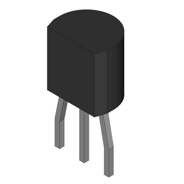
Figure 1
TLV4961-3T in the TO92S-3-1 and TO92S-3-2 package
1.2
Features
•
3.0 V to 26 V operating supply voltage
•
Operation from unregulated power supply
•
Output overcurrent and overtemperature protection
•
Active error compensation
•
High stability of magnetic thresholds
•
High ESD performance
•
Leaded, halogen-free package TO92S-3-1 for TLV4961-3TA,
TO92S-3-2 for TLV4961-3TB
For automotive applications please refer to the Infineon TLE Hall Switches/Latches series.
Table 1
Ordering information
Product name
Product type
Ordering code
Package
TLV4961-3TA
Bipolar Hall Latch
SP001274776
TO92S-3-1 (Bulk)
TLV4961-3TB
Bipolar Hall Latch
SP001283606
TO92S-3-2 (Ammo pack)
1) Only the package is halogen-free.
Data Sheet
5
Revision 1.2, 2019-12-20
�TLV4961-3T
Product description
1.3
Target applications
Target applications for the TLV496x Hall Latch family are all applications which require a high precision
Hall Latch with an operating temperature range from -40°C to 125°C.
The magnetic behavior as a latch and switching thresholds of typical ±7.5 mT make the device especially
suited for the use with a pole wheel for index counting applications, for rotor position detection as in brushless
DC motor commutation and for white goods or open/closing detection.
Data Sheet
6
Revision 1.2, 2019-12-20
�TLV4961-3T
Functional description
2
Functional description
2.1
General
The TLV4961-3T is an integrated Hall effect latch designed specifically for highly accurate applications with
superior supply voltage capability and temperature stability of the magnetic thresholds.
2.2
Pin configuration (top view)
1
VDD
2
GND
3
Q
Figure 2
Pin configuration and center of sensitive area
2.3
Pin description
Table 2
Pin description
Pin no.
Symbol
Function
1
VDD
Supply voltage
2
GND
Ground
3
Q
Output
Data Sheet
7
Revision 1.2, 2019-12-20
�TLV4961-3T
Functional description
2.4
Block diagram
VDD
To All Subcircuits
Voltage
Regulator
Oscillator and
Sequencer
Bias and
Compensation
Circuits
Spinning Hall
Probe
Amplifier
Demodulator
Chopper
Multiplexer
Reference
Q
Control
Low Pass
Filter
Comparator
with
Hysteresis
Overtemperature
& overcurrent
protection
GND
Figure 3
Data Sheet
Functional block diagram TLV4961-3T
8
Revision 1.2, 2019-12-20
�TLV4961-3T
Functional description
2.5
Functional block description
The chopped Hall IC switch comprises a Hall probe, bias generator, compensation circuits, oscillator and
output transistor.
The bias generator provides currents for the Hall probe and the active circuits. Compensation circuits stabilize
the temperature behavior and reduce influence of technology variations.
The active error compensation (chopping technique) rejects offsets in the signal path and the influence of
mechanical stress to the Hall probe caused by molding and soldering processes and other thermal stress in
the package. The chopped measurement principle together with the threshold generator and the comparator
ensures highly accurate and temperature stable magnetic thresholds.
The output transistor has an integrated overcurrent and overtemperature protection.
B OP
Applied
Magnetic
Field
BR P
td
td
tf
tr
VQ
90%
10%
Figure 4
Timing diagram TLV4961-3T
VQ
B
BRP
Figure 5
Data Sheet
0
BOP
Output signal TLV4961-3T
9
Revision 1.2, 2019-12-20
�TLV4961-3T
Functional description
2.6
Default start-up behavior
The magnetic thresholds exhibit a hysteresis BHYS = BOP - BRP. In case of a power-on with a magnetic field B
within hysteresis (BOP > B > BRP) the output of the sensor is set to the pull up voltage level (VQ) per default. After
the first crossing of BOP or BRP of the magnetic field the internal decision logic is set to the corresponding
magnetic input value.
VDDA is the internal supply voltage which is following the external supply voltage VDD.
This means for B > BOP the output is switching, for B < BRP and BOP > B > BRP the output stays at VQ.
VDDA
tPon
3V
The device always applies
VQ level at start -up
Power on ramp
VQ
t
independent from the
applied magnetic field !
Magnetic field above threshold
B > BOP
t
VQ
Magnetic field below threshold
B < BRP
t
VQ
Magnetic field in hysteresis
BOP > B > BRP
t
Figure 6
Data Sheet
Start-up behavior of the TLV4961-3T
10
Revision 1.2, 2019-12-20
�TLV4961-3T
Specification
3
Specification
3.1
Application circuit
The following Figure 7 shows the basic option of an application circuit. Only a pull-up resistor RQ is necessary.
The resistor RQ has to be in a dimension to match the applied VS to keep IQ limited to the operating range of
maximum 25 mA.
e.g.: VS = 12 V; IQ = 12 V/1200 Ω = 10 mA
Vs
VDD
TLV496x
TLE4963-1M
RQ = 1.2kΩ
Q
GND
Figure 7
Basic application circuit #1: only pull-up resistor is necessary
Vs
CDD = 47nF
TLV496x
VDD
RQ = 1.2kΩ
Q
TVS diode
e.g. ESD24VS2U
GND
Figure 8
Enhanced application circuit #2: for extended ESD robustness
With an additional capacitor CDD and a transient voltage suppression (TVS) diode an extended ESD robustness
on system level is achieved (Figure 8).
Data Sheet
11
Revision 1.2, 2019-12-20
�TLV4961-3T
Specification
3.2
Absolute maximum ratings
Table 3
Absolute maximum rating parameters
Parameter
Symbol
1)
Values
Min.
Typ.
Max.
Unit
Note or Test Condition
Supply voltage
VDD
3
–
26
V
–
Output voltage
VQ
-0.5
–
26
V
–
Reverse output current
IQ
-70
–
–
mA
–
1)
Junction temperature
TJ
-40
–
150
°C
–
Storage temperature
TS
-40
–
150
°C
–
Thermal resistance
Junction ambient
RthJA
–
–
250
K/W
for TO92S-3-1, TO92S-3-2 (2s2p)
1) This lifetime statement is an anticipation based on an extrapolation of Infineon’s qualification test results. The actual
lifetime of a component depends on its form of application and type of use etc. and may deviate from such statement.
The lifetime statement shall in no event extend the agreed warranty period.
Attention: Stresses above the max. values listed here may cause permanent damage to the device.
Exposure to absolute maximum rating conditions for extended periods may affect device
reliability. Maximum ratings are absolute ratings; exceeding only one of these values may
cause irreversible damage to the integrated circuit.
Calculation of the dissipated power PDIS and junction temperature TJ of the chip (TO92S example):
e.g. for: VDD = 12 V, IS = 2.5 mA, VQSAT = 0.5 V, IQ = 20 mA
Power dissipation: PDIS = 12 V x 2.5 mA + 0.5 V x 20 mA = 30 mW + 10 mW = 40 mW
Temperature ∆T = RthJA x PDIS = 250 K/W x 40 mW = 10 K
For TA = 50°C: TJ = TA + ∆T = 50°C + 10 K = 60°C
Data Sheet
12
Revision 1.2, 2019-12-20
�TLV4961-3T
Specification
Table 4
ESD protection1) (TA = 25°C)
Parameter
Symbol
2)
3)
ESD voltage (HBM)
ESD voltage (CDM)
Values
Unit
Note or Test Condition
Min.
Typ.
Max.
VESD
-4
–
4
kV
R = 1.5 kΩ, C = 100 pF
VESD
-1
–
1
kV
–
1) Characterization of ESD is carried out on a sample basis, not subject to production test.
2) Human Body Model (HBM) tests according to ANSI/ESDA/JEDEC JS-001.
3) Charge device model (CDM) tests according to JESD22-C101.
3.3
Operating range
The following operating conditions must not be exceeded in order to ensure correct operation of
the TLV4961-3T.
All parameters specified in the following sections refer to these operating conditions unless otherwise
mentioned.
The maximum tested magnetic field is 600 mT.
Table 5
Operating conditions parameters
Parameter
Symbol
Values
Min.
Typ.
Max.
Unit
Note or
Test Condition
Supply voltage
VDD
3.0
–
261)
V
–
Output voltage
VQ
3.0
–
26
V
–
Operation temperature
TA
-40
–
125
°C
RthJA ≤ 250 K/W
Output current
IQ
0
–
25
mA
–
1) Latch-up test with factor 1.5 is not covered. Please see max ratings also.
Data Sheet
13
Revision 1.2, 2019-12-20
�TLV4961-3T
Specification
3.4
Electrical and magnetic characteristics
Product characteristics involve the spread of values guaranteed within the specified voltage and ambient
temperature range. Typical characteristics are the median of the production and correspond to VDD = 12 V and
TA = 25°C. The below listed specification is valid in combination with the application circuit shown in Figure 7
and Figure 8.
Table 6
General electrical characteristics
Parameter
Symbol
Values
Min.
Typ.
Max.
Unit
Note or Test Condition
Supply current
IS
1.1
1.6
2.5
mA
–
Output current limitation
IQLIMIT
30
56
70
mA
internally limited and thermal
shutdown
Output fall time1)
tf
0.17
0.4
1
μs
1.2 kΩ / 50 pF, see Figure 4
1)
tr
0.4
0.5
1
μs
1.2 kΩ / 50 pF, see Figure 4
td
12
15
30
μs
see Figure 4
tPON
–
80
150
μs
VDD = 3 V, B ≤ BRP - 0.5 mT or
B ≥ BOP + 0.5 mT
Output rise time
Delay time
1)2)
Power-on time1)3)
1) Not subject to production test, verified by design/characterization.
2) Systematic delay between magnetic threshold reached and output switching.
3) Time from applying VDD = 3.0 V to the sensor until the output is valid.
Data Sheet
14
Revision 1.2, 2019-12-20
�TLV4961-3T
Specification
Table 7
Magnetic characteristics
Parameter
Symbol
Operating point
Release point
Hysteresis
BOP
BRP
BHYS
Temperature compensation of TC
magnetic thresholds1)
T (°C)
Values
Min.
Typ.
Max.
-40
5.2
8.4
11.5
25
4.6
7.5
10.4
125
3.6
6.2
8.7
-40
-11.5
-8.4
-5.2
25
-10.4
-7.5
-4.6
125
-8.7
-6.2
-3.6
-40
12.4
16.8
22.9
25
11.2
15.0
20.8
125
9.2
12.3
17.4
–
–
-1800
–
Unit
Note / Test
Condition
mT
–
mT
–
mT
–
ppm/K –
1) Not subject to production test, verified by design/characterization.
Field direction definition
Positive magnetic fields are defined with the south pole of the magnet to the branded side of package.
N
Branded Side
Figure 9
Data Sheet
S
Definition of magnetic field direction TO92S-3-1, TO92S-3-2
15
Revision 1.2, 2019-12-20
�TLV4961-3T
Package information
4
Package information
The TLV4961-3TA is available in Bulk packing with TO92S-3-1-package.
The TLV4961-3TB is available in AMMO packing with TO92S-3-2-package.
4.1
Package outline
Figure 10
Package outline TLV4961-3TA: TO92S-3-1 (all dimensions in mm)
Data Sheet
16
Revision 1.2, 2019-12-20
�TLV4961-3T
Package information
Figure 11
Data Sheet
Package outline TLV4961-3TB: TO92S-3-2 (all dimensions in mm)
17
Revision 1.2, 2019-12-20
�TLV4961-3T
Package information
4.2
Packing information
Figure 12
Packing information
4.3
Distance between chip and package
Figure 13
Distance between chip and package
Data Sheet
18
Revision 1.2, 2019-12-20
�TLV4961-3T
Package information
4.4
Package marking
Halogen free (H)
Year (Y) = 0...9
Calendar Week (WW) = 01...52
Lot Code (LL)
HYWWLL
V613T
Figure 14
Data Sheet
Marking of TLV4961-3T
19
Revision 1.2, 2019-12-20
�TLV4961-3T
Revision history
5
Revision history
Revision
Date
Changes
Revision 1.2
2019-12-20
Updated text and figure in Chapter 2.6
Updated standards in Table 4
Added maximum tested magnetic field in Chapter 3.3
Editorial changes
Revision 1.0
2015-05-18
Initial release
Data Sheet
20
Revision 1.2 2019-12-20
�Trademarks
All referenced product or service names and trademarks are the property of their respective owners.
www.infineon.com
Edition 2019-12-20
Published by
Infineon Technologies AG
81726 Munich, Germany
© 2019 Infineon Technologies AG.
All Rights Reserved.
Do you have a question about any
aspect of this document?
Email: erratum@infineon.com
Document reference
Legal Disclaimer
The information given in this document shall in
no event be regarded as a guarantee of
conditions or characteristics. With respect to any
examples or hints given herein, any typical
values stated herein and/or any information
regarding the application of the device, Infineon
Technologies hereby disclaims any and all
warranties and liabilities of any kind, including
without limitation, warranties of noninfringement of intellectual property rights of
any third party.
Information
For further information on technology, delivery
terms and conditions and prices, please contact
the nearest Infineon Technologies Office
(www.infineon.com).
Warnings
Due to technical requirements, components
may contain dangerous substances. For
information on the types in question, please
contact the nearest Infineon Technologies
Office. Infineon Technologies components may
be used in life-support devices or systems only
with the express written approval of Infineon
Technologies, if a failure of such components
can reasonably be expected to cause the failure
of that life-support device or system or to affect
the safety or effectiveness of that device or
system. Life support devices or systems are
intended to be implanted in the human body or
to support and/or maintain and sustain and/or
protect human life. If they fail, it is reasonable to
assume that the health of the user or other
persons may be endangered.
�