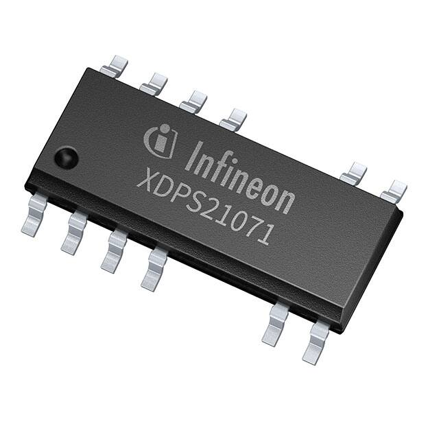
XDPS21071
Forced Frequency Resonant Flyback controller
Based on FW: REV 1.0
Product Highlights
•
•
•
•
•
•
Integrated 600 V startup cell for fast startup and direct bus voltage sensing
Multi-mode operation with forced frequency resonant mode (FFR)
DCM operation guaranteed
Adaptive current limitation for variable Vout
Supports low no load input power to meet stringent regulatory standard
One pin UART interface for configuration
Features
Description
• Multi-mode operation with BM, DCM
• Configurable ZVS enabled line voltage
• ZVS gate drive signal for forced resonant mode
• Built-in soft-start
• Built-in protection modes
• Brown-in and brownout detection via integrated HV
startup cell
• Pb-free lead plating; RoHS compliant
• Halogen-free according to IEC61249-2-21
The XDPS21071 is a digital PWM controller for high density
adapter applications based on DCM flyback topology. A wide
feature set is provided in a DSO-12 package and requires
only a minimum of external components. An integrated
ASSP digital engine provides advanced algorithms for multimode operation and protection features. A forced frequency
resonant operation support optimized high density adapter
system dimensioning. In addition a one-timeprogrammable (OTP) unit is integrated to provide a
selective set of configurable parameters, which can be
matched to a dedicated system design.
Applications
•
High density adapter/charger
Product Validation
•
Qualified for industrial applications according to the
relevant tests of JEDEC47/20/22
85 ... 264 VAC
VCC
ZCD
GD1
HV
GPIO
GD0
XDPS21071 CS
MFIO
GND
Figure 1
Typical application
Marking
Package
FW Revision
SP Ordering Code
XDPS21071
PG-DSO-12-20
REV 1.0
SP005355100
Data Sheet
www.infineon.com
Please read the Important Notice and Warnings at the end of this document
Revision 2.0
2019-10-30
�Forced Frequency Resonant Flyback controller
Table of contents
Description
Table
of contents
Description
Description
Based on FW: REV 1.0 ...................................................................................................................... 1
Product Highlights .......................................................................................................................... 1
Description
Features 1
Applications ................................................................................................................................... 1
Description
Product Validation .......................................................................................................................... 1
Description 1
Table of contents ............................................................................................................................ 2
1
Pin Configuration and Functionality ................................................................................ 4
2
Representative Block Diagram ........................................................................................ 5
3
Introduction.................................................................................................................. 6
4
4.1
4.1.1
4.1.2
4.1.3
4.1.4
4.1.5
4.1.5.1
4.1.5.2
4.2
4.2.1
4.2.1.1
4.2.1.2
4.2.1.3
4.2.2
4.2.3
4.2.4
4.2.5
4.2.6
4.2.7
4.2.8
4.2.8.1
4.2.9
4.2.10
4.2.10.1
4.2.10.2
4.2.11
4.2.12
4.2.13
4.3
4.3.1
4.3.2
4.3.3
4.3.4
4.3.5
4.3.6
Functional Description ................................................................................................... 7
Power supply management .................................................................................................................... 7
VCC capacitor charge-up and startup sequence............................................................................... 7
Brown-in monitoring.......................................................................................................................... 8
Brown-out protection response ........................................................................................................ 9
During burst mode operation ........................................................................................................... 9
Bang-bang mode during latched and auto-restart operation ....................................................... 10
During latched operation............................................................................................................ 11
During auto-restart operation .................................................................................................... 11
Control features..................................................................................................................................... 12
Reflected voltage sensing and Vcs offset calculation based on output voltage............................ 14
Output voltage sensing via ZCD pin ........................................................................................... 15
Ringing suppression time ........................................................................................................... 17
Vcs offset calculation based on output voltage sensed at ZCD pin .......................................... 17
Vbulk voltage measurement via HV startup cell ............................................................................. 18
Propagation delay compensation (PDC) ......................................................................................... 18
Soft-start........................................................................................................................................... 20
Leading edge blanking (LEB) at CS pin ............................................................................................ 20
Spike blanking at CS pin for 2nd level over-current detection (OCP2) .......................................... 21
Gate driver output GD0 and GD1 ..................................................................................................... 21
Multi-mode operation ...................................................................................................................... 22
Frequency law setting for XDPS21071 ........................................................................................ 24
Frequency jittering ........................................................................................................................... 25
Burst mode operation ...................................................................................................................... 26
Burst mode entry ........................................................................................................................ 27
Burst operation ........................................................................................................................... 27
Burst mode exit ................................................................................................................................ 28
Forced frequency resonant (FFR) mode operation......................................................................... 28
UART function at GPIO pin ............................................................................................................... 30
Protection features ............................................................................................................................... 30
Auto-Restart Mode (ARM) ................................................................................................................. 31
Latch Mode (LM) ............................................................................................................................... 31
VCC Under-Voltage lockout (UVOFF) ............................................................................................... 31
Brown-In Protection (BIP) ................................................................................................................ 31
Brown-Out Protection (BOP) ........................................................................................................... 32
Over-Current Protection level 1 (OCP1) .......................................................................................... 32
Data Sheet
2
Revision 2.0
2019-10-30
�Forced Frequency Resonant Flyback controller
Table of contents
4.3.7
4.3.8
4.3.9
4.3.10
4.3.11
4.3.12
4.3.13
Over-Current Protection level 2 (OCP2) .......................................................................................... 32
High input at CS pin (CShigh) .......................................................................................................... 32
MFIO pin high (MFIOH) ..................................................................................................................... 32
Internal over-temperature detection (IntOTP) ............................................................................... 32
Primary side output Over-Voltage Protection (VoutOVP)............................................................... 33
Over load power protection............................................................................................................. 33
CS pin short protection .................................................................................................................... 33
5
5.1
5.2
5.2.1
Configuration ............................................................................................................... 34
Overview of configurable parameters using .dp Vision ....................................................................... 34
Overview of configurable parameters and functions .......................................................................... 34
Configurable parameters and functions ......................................................................................... 34
6
6.1
6.2
6.3
6.4
6.5
Electrical Characteristics ............................................................................................... 36
Definitions ............................................................................................................................................. 36
Absolute Maximum Ratings .................................................................................................................. 36
Package Characteristics ........................................................................................................................ 37
Operating Range.................................................................................................................................... 38
Characteristics ....................................................................................................................................... 39
7
7.1
7.2
Package Information ..................................................................................................... 48
Outline dimensions ............................................................................................................................... 48
Footprint and packing........................................................................................................................... 49
8
Marking ....................................................................................................................... 50
9
9.1
Appendix ..................................................................................................................... 51
Minimum required capacitive load at GD0 and GD1 pin ...................................................................... 51
10
References ................................................................................................................... 52
Revision history............................................................................................................................. 53
Data Sheet
3
Revision 2.0
2019-10-30
�Forced Frequency Resonant Flyback controller
Pin Configuration and Functionality
1
Pin Configuration and Functionality
The pin configuration is shown in Figure 2 and the functions are described in Table 1.
1
12
GND
MFIO
2
11
VCC
GPIO
3
10
GD0
CS
4
9
GD1
HV
5
8
HV
6
HV
HV
XDPS21071
ZCD
7
PG-DSO-12-20
Figure 2
Pin Configuration of XDPS21071
Table 1
Pin Definitions and Functions
Symbol
ZCD
Pin
Type
1
I
Function
Zero Crossing Detection
ZCD pin is connected to an auxiliary winding for zero crossing detection and positive
pin voltage measurement.
MFIO
2
I
Multi-Functional Input Output
MFIO pin is connected to an optocoupler that provides an amplified error signal for
the PWM mode operation.
GPIO
3
IO
CS
4
I
HV
5, 6, 7, 8 I
GD1
9
I
GD0
10
O
VCC
11
I
GND
12
O
Data Sheet
Digital General Purpose Input Output
GPIO pin provides an UART interface until brown-in. It is switched to weak
pull down mode and disabled UART function during normal operation.
Current Sense
CS pin is connected via a resistor in series to an external shunt resistor and
the source of the power MOSFET.
High Voltage Input
HV pin is connected to the rectified bulk voltage. An internally connected 600
V HV startup-cell is used for initial VCC charge. Furthermore brown-in and
brownout detection is provided.
FFR Signal Gate Driver Output
GD1 pin provides a gate driver pulse signal to initiate the forced frequency
resonant mode operation.
Gate Driver Output
Output for directly driving the main power MOSFET.
Positive Voltage Supply
IC power supply.
Power and Signal Ground
4
Revision 2.0
2019-10-30
�Forced Frequency Resonant Flyback controller
Representative Block Diagram
2
Representative Block Diagram
Figure 3 shows a simplified top level block diagram of the IC functionality.
XDPS21071
HV
HV Startup-cell
Bang-Bang Ctrl
Startup-Cell
Driver
Closed/Open
VVCCBBoff = 20.5 V
VVCCBBonAR/LM = 9 V
Vbulk Brown-out
Protection
QM
IHVBO = 0.443 mA
D1
Vbulk
measurement
Vbulk Brown-in
Protection
Overtemperature
Detection
IHVBI = 1.15 mA
RM
VCC Brown-in
Protection
VCC
TJOTP = 130 °C
&
VVCCBI = 9.1 V
Protection
Modes
HW Reset
UVLO
VVCCon = 20.5 V
Power
Management
VVCCoffx = 7.2 V / 9.6 V
Vout OV
Protection
Vout reflected Voltage
Measurement
ZCD
1k
Auto Restart
Mode
Latch
Mode
VZCDOVP = 2.75 V
Soft-Start
Open Loop Timer
tMFIOH = 31.3 ms
Frequency clamp
fSW
VMFIOH = 2.41 V
VCSPK
C2
FFR Mode
With ZVS Pulse
Generation
Frequency Law
PWM
Logic
Gate Driver
GD0
VMFIO
PDC
VVDDP = 3.3 V
VMFIO
Gate Driver
RMFIOPU
GD1
Vcs_offset
Burst Mode Function
MFIO
VMFIOBMEX1
VMFIOBMWK
C3
BM Exit
C5
on-phase
VMFIOBMPA
VMFIOBMEN
C6
off-phase
C7
BM 2-point
Regulation
BM Ctrl
BM Entry
Cycle by Cycle Peak Current Ctrl
OCP1
CS
1k
10k
VCSPK
1 pF
tCSLEB
2nd Level Overcurrent Detection
OCP2
Auto Restart
Input Detection
tCSOCP2BL
VCSOCP2 = 0.8 V
VVDDP = 3.3 V
IGPIOLPU
GPIO
Figure 3
Data Sheet
UART
Communication
Parameter
Configuration
Representative Block Diagram of XDPS21071
5
Revision 2.0
2019-10-30
�Forced Frequency Resonant Flyback controller
Introduction
3
Introduction
The XDPS21071 is a digital AC/DC current-mode controller for high density adapter applications. The IC provides a
configurable multi-mode operation controlled by the feedback signal from the secondary side control loop. The multi-mode
operation supports different operation modes like forced frequency resonant control (see chapter 4.2.12) or burst mode,
frequency reduction mode depending on line and load conditions. With supporting those modes high power density designs
can be dressed in a very flexible manner.
An embedded application specific digital core provides advanced algorithms for the multi-mode operation and a variety of
protection features. Special analog and mixed-signal peripherals are integrated to support the requirements for low standby power.
The IC supports highest design flexibility in the application by means of an advanced set of configurable parameters and
state machines, which supports very dedicated system dimensioning. The configuration can be done via a single pin UART
interface at GPIO pin that supports in-circuit configuration. Chapter 5 contains the parameter default configuration setting
for XDPS21071 and the correlated specific firmware version. Furthermore, it provides a mapping table for the defined FW
symbols and the correlated data sheet parameters. Each listed parameter is specified in the electrical characteristics
Chapter 6.
The following functional description in Chapter 4 is based on the default parameter setting in the configuration Chapter 5.
Chapter 7.1 provides information about the package outline and dimensions.
An appendix Chapter 9 provides additional information about specific electrical characteristics or test conditions.
The reference Chapter 10 provides an overview about correlated documents.
Data Sheet
6
Revision 2.0
2019-10-30
�Forced Frequency Resonant Flyback controller
Functional Description
4
Functional Description
The functional description gives an overview about the integrated functions and features and their relationship. The
mentioned parameters and equations are based on typical values at TA = 25 °C. The correlated minimal and maximal values
are shown in the electrical characteristics in Chapter 6.
The functional description is grouped in following sections:
Power supply management (Chapter 4.1)
Control features (Chapter 4.2)
Protection features (Chapter 4.3)
4.1
Power supply management
The power supply management ensures a reliable and robust IC operation. Depending on the operation mode of the control
IC, the power supply management unit runs in different ways for VCC supply and for brown-in monitoring, which are
described in the sequel:
•
•
•
•
•
•
VCC capacitor charge-up and startup sequence (see Chapter 4.1.1)
Brown-in monitoring (Chapter 4.1.2)
Brown-out protection response (Chapter 4.1.3)
During burst mode (QBM) operation (Chapter 4.1.4)
Bang-bang mode during latch mode (LM) operation (Chapter 4.1.5.1 )
Bang-bang mode during auto-restart mode (ARM) operation (Chapter 4.1.5.2)
4.1.1
VCC capacitor charge-up and startup sequence
There are two main functions supported at HV pin by a resistor RHV connected to the bulk capacitor (see Figure 5). They are
the VCC capacitor charge-up, and the bulk voltage monitoring (see Chapter 4.1.2).
At beginning of a cold startup, the depletion startup cell is on. Once the AC line voltage is applied and charging the bulk
capacitor, a current flows through the external resistor RHV into HV pin. Via the integrated diode D1, that current may charge
up the external VCC capacitor (see Figure 5). Once VCC voltage exceeds the threshold VVCCon = 20.5 V, the startup cell is turned
off, the control IC is enabled and the firmware boot sequence follows which takes about 1.2 ms. Both bulk voltage brown-in
and VCC brown-in condition (see Chapter 4.3.4) are checked continuously. Once they both are above the brown-in level,
respectively, the first GD0 pulse according to the soft-start control will be generated earliest after the 1.2 ms boot sequence
time. The voltage VVCC drops until the supply via the auxiliary winding (VVCCSS) takes over the VCC supply (see Figure 4). For a
proper system startup and operation, the supply voltage VVCC must be always above the VCC off-threshold VVCCoff=7.2 V (see
Chapter 4.3.3).
Data Sheet
7
Revision 2.0
2019-10-30
�Forced Frequency Resonant Flyback controller
Functional Description
VVCC(t)
Initial startup and normal operation
VVCCon = 20.5 V
VCC brown-in window
VVCCSS
VVCCBI = 9.1 V
VVCCoffOP = 7.2 V
VCC self supply takes over
t
VHV(t)
ca. 1.2ms internal boot sequence
VVACpeak
VAC brown-in condition fulfilled
t
IVCC(t)
Start of GD0 switching
IVCCop
IVCCop1 = 7.5 mA
IVCCUVOFF = 30 µA
t
TYPICAL STARTUP SEQUENCE
Figure 4
Typical startup sequence
4.1.2
Brown-in monitoring
Once the IC is activated, brown-in monitoring is enabled for input brown-in protection (see Chapter 4.3.4) by measuring
the current at HV pin through the internal shunt resistor RM (see Chapter 4.2.2). If the input brown-in is not detected before
VCC falls below VVCCBI, the startup cell measurement unit remains enabled until VCC falls down to VVCCoff.
Data Sheet
8
Revision 2.0
2019-10-30
�Forced Frequency Resonant Flyback controller
Functional Description
VBULK
VAC = 85 ... 264
Vrms
CBulk
RHV = 100kW
CVCC
VCC
HV
HV Startupcell
Closed/Open
Startup-Cell
Driver
D1
Brown-in &
Brown-out
Protection
QM
IHVBI = 1.15 mA
IHVBO = 0.442mA
&
PWM
Logic
RM
VCC Brown-in
Protection
VVCCBI = 9.1 V
Power Supply
Management
UVLO
VVCCon = 20.5 V
HW Reset
VVCCoffx = 7.2 V / 9.6 V
Figure 5
High voltage brown-in sensing and VCC startup at HV pin
4.1.3
Brown-out protection response
In case of brown-out (see Chapter 4.3.5), the IC stops gate driver switching and stays active. At the same time, the VCC turnoff threshold is switched over from VVCCoff to the threshold VVCCoffBO = 9.6 V. The threshold VVCCoffBO is higher than the threshold
VVCCoff, which supports an earlier system restart than using the threshold VVCCoff.
4.1.4
During burst mode operation
After the control IC enters quiet burst mode, the IC enters repeatedly a sleep mode, in which the IC current consumption is
reduced to IVCCquBM2 = 460 µA. Waking up from and entering this sleep mode (pause) is controlled by the feedback voltage at
MFIO pin VMFIO via the internal comparators C5 and C6 (see Figure 6 and Chapter 4.2.910).
Data Sheet
9
Revision 2.0
2019-10-30
�Forced Frequency Resonant Flyback controller
Functional Description
MFIO
C5
VMFIOBMWK
C6
burst-on
BM 2-point
Regulation
burst-off
Power
Management
BM Ctrl
VMFIOBMPA
Figure 6
Burst mode control
For the system dimensioning, it should be ensured that the voltage VVCC should be always well above the
threshold VVCCoff, including the burst-off phase. Figure 7 shows a typical burst mode operation signal for VCC and
correlated current consumption.
VVCC(t)
burst-on phase
VVCCSS
VVCCoff = 7.2 V
t
VMFIO(t)
burst-off phase
VMFIOBMWK = 1.6 V
VMFIOBMPA
t
VGD0(t)
t
IVCC(t)
IVCCop
IVCCquBM2 = 460 µA
t
Figure 7
Burst operation
4.1.5
Bang-bang mode during latched and auto-restart operation
The bang-bang mode supports an IC operation without external VCC supply during the latched and auto-restart operation.
It directly controls the HV startup cell depending on the set bang-bang mode turn-on threshold VVCCBBon of the corresponding
auto-restart and latch mode (see Figure 8). In latch mode, the HV startup cell switch-on threshold is set to VVCCBBon = 9 V (see
Chapter 4.1.5.1 and Chapter 4.1.5.2). In auto-restart mode, there is also an additional stand-by timer active that switches on
the HV startup cell in a fixed time period of 500ms scheme to keep the VCC all the time at a high level above the brown-in
threshold VVCCBI = 9.1 V. Then a restart can take place without going through an additional VCC brown-in cycle. Due to the low
current consumption during the auto-restart break time, the startup cell is always turned on by the 500 ms timer.
Protection Modes
HV
HV Startup-cell
Closed/Open
Bang-Bang Ctrl
Startup-Cell
Driver
Auto Restart
Mode
VVCCBBoff = 20.5 V
VVCCBBonAR/LM = 9 V
Latch
Mode
D1
Power
Management
VCC
Figure 8
Data Sheet
Bang-bang mode control of HV startup-cell
10
Revision 2.0
2019-10-30
�Forced Frequency Resonant Flyback controller
Functional Description
4.1.5.1
During latched operation
If latch mode is entered (see Chapter 4.3.2), the IC stops gate switching and the VCC current consumption is reduced to
IVCCquLM = 150 µA. The enabled bang-bang mode ensures that the IC is kept alive by keeping the voltage at VCC pin above the
threshold VVCCoff = 7.2 V (see Figure 9). A reset of the latch mode takes place only after the VCC drops below the VVCCoff threshold.
VVCC(t)
Latch mode operation
VVCCBBoff = 20.5 V
VVCCSS
VVCCBBonLM = 9 V
VVCCoff = 7.2 V
Reset of latch mode due to low VAC
VHV(t)
t
VVACpeak
t
IVCC(t)
IVCCop
IVCCquLM = 150 µA
IVCCUVOFF = 30 µA
Figure 9
4.1.5.2
t
Latch mode operation
During auto-restart operation
Once auto-restart mode is entered (see Chapter 4.3.1), the IC stops GD0 switching, the VCC current consumption is reduced
to IVCCquAR = 160 µA, and a stand-by timer with 500 ms (tBBoffAR) period is activated which turns on the HV startup cell
periodically, to charge up the VCC capacitor. Once the voltage at VCC pin exceeds the switch-off threshold VVCCBBoff = 20.5 V,
the startup cell is turned off (see Figure 10). This is bang-bang mode operation for the VCC management during the autorestart break time. In this way, the VCC voltage is kept at a level well above the VCC brown-in threshold to ensure enough
energy stored in the VCC capacitor for the coming restart of the system, that is initiated after the auto-restart break time
tAR = 3 s. Then after an additional time ∆t = ε, the gate driver switching is activated with a soft-start sequence. Here the
additional time ε depends on the VCC capacitor charge-up time which is related to the VCC capacitance and the voltage at
HV pin.
Data Sheet
11
Revision 2.0
2019-10-30
�Forced Frequency Resonant Flyback controller
Functional Description
VVCC(t)
Auto-restart mode operation
VVCCBBoff = 20.5 V
VVCCSS
VVCCBI = 9.1 V
VVCCBBonAR = 9 V
VVCCoff = 7.2 V
t
tBBoffAR = 500 ms
VHV(t)
VVACpeak
Dt = e
t
IVCC(t)
IVCCop
IVCCop1 = 7.5 mA
IVCCquAR = 160 µA
t
VGD0(t)
tAR = 3s
VGD0H = 10.5 V
t
Figure 10
4.2
Auto-restart mode operation
Control features
The XDPS21071 provides peak current control assisted by the features listed in Table 2. A simplified block diagram
representing the controller features is shown in Figure 11.
Data Sheet
12
Revision 2.0
2019-10-30
�Forced Frequency Resonant Flyback controller
Functional Description
CS
tCSOCP2BL
VCSOCP2
VCS
FF
Cold Start,
BM Wake-Up,
Autorestart
Soft-Start
Control
VVDDP
HV
VMFIO
frequency law,
burst mode control
IHV
VBulk
Measurment
&
SET
&
+
VCSOCP1
stop GD0
VCSSS
M
I
N
Multi-Mode
Control
MFIO
GD0
CLEAR
+
&
tCSLEB
CLEAR
FF
SET
Propagation
Delay
Compensation
tZCDRS
Vcs_offset
start GD0
Start Request
Generator
ZCD
Vout
Measurement
fSW
FFR ZVS
PWM
Generator
GD1
ZCD
MULTIMODE_OVERVIEW_DIGITAL
Figure 11
Block Diagram of PWM Control
Table 2 gives an overview about the controller features that are described in the mentioned chapters.
Table 2
Controller Features
Reflected voltage sensing and zero crossing detection at auxiliary winding
Chapter 4.2.1
Vbulk voltage measurement via HV startup cell
Chapter 4.2.2
Propagation delay compensation (PDC)
Chapter 4.2.3
Soft-start
Chapter 4.2.4
Leading edge blanking (LEB) time at CS pin
Chapter 4.2.5
Spike blanking at CS pin for 2nd level over-current detection
Chapter 4.2.6
Gate driver output GD0 and GD1
Chapter 4.2.7
Multi-mode operation
Chapter 4.2.8
Burst mode (QBM) operation
Chapter 4.2.9
Forced frequency resonant (FFR) mode operation
Chapter 4.2.12
UART function at GPIO pin
Chapter 4.2.13
Data Sheet
13
Revision 2.0
2019-10-30
�Forced Frequency Resonant Flyback controller
Functional Description
4.2.1
Reflected voltage sensing and Vcs offset calculation based on
output voltage
The IC provides output voltage detection by means of measuring the reflected voltage at the auxiliary winding VAux at the
primary side of the transformer via ZCD pin and an external resistive voltage divider. The voltage signal VAux contains the
information of the flyback output voltage, VOut, at the secondary side.
The ZCD pin related circuit is shown in Figure 12. Figure 13 shows a typical voltage waveform of the drain voltage VDrain and
the related auxiliary winding voltage VAux. The sensed output voltage is used for over-voltage protection (see Chapter 4.3.11).
Following topics are described in the sequel:
•
•
Output voltage sensing via ZCD pin (Chapter 4.2.1.1)
Vcs offset with sensed Vo at ZCD pin (Chapter 4.2.1.3)
vPri
vSec
VOu t
VBulk
vDrain
RZCDH
iZCD
vAux
RZCDL
ZCD
vZCD
GND
vZVS
VOLTAGE_SENSING_OVERVIEW
Figure 12
Data Sheet
Functionality at ZCD pin
14
Revision 2.0
2019-10-30
�Forced Frequency Resonant Flyback controller
Functional Description
vDrain (t)
NPri / NSec × vSec
VBulk
0
t
Free-wheeling phase
vAux(t)
Oscillation phase
NAux / NSec × vSec
0
t
NAux / NPri × VBulk
1 1 1 1
4 4 4 4
tOn
tf
tOsc
tOff
iMag(t)
t
VOLTAGE_SENSING_SIGNALS
Figure 13
Auxiliary voltage and magnetization current waveforms for standard discontinuous
conduction mode operation
4.2.1.1
Output voltage sensing via ZCD pin
Output voltage is sensed at a fixed point of time during the free-wheeling phase. The free-wheeling phase begins when the
gate driver is switched off and ends when the secondary side demagnetization current becomes zero. During free-wheeling
phase the VCC capacitor of the IC, the output stage and the additional ZVS capacitor at ZVS winding for introducing a forced
resonant cycle (see Chapter 4.2.12) are supplied. As soon as VCC capacitor is charged, the auxiliary voltage is a function of
secondary side voltage.
𝑽𝑨𝑼𝑿 =
𝑵𝑨𝑼𝑿
𝑵𝑺𝒆𝒄
(1)
∙ 𝑽𝑺𝒆𝒄
Figure 14 shows the schematic related to secondary side voltage sensing and the equivalent network.
Data Sheet
15
Revision 2.0
2019-10-30
�Forced Frequency Resonant Flyback controller
Functional Description
NSec :NAux
RZCDH
vSec (t)
iZCD=0
vAux(t)
RZCDL
ZCD
vZCD>0
GND
ZCD
vZCDSEC (vSec )
+
GND
VOLTAGE_SENSING_ZCDSH
Figure 14
Secondary Side Voltage Sensing
No current clamping applies during the free-wheeling time and the voltage at ZCD pin is given by
𝑽𝒁𝑪𝑫𝑺𝑬𝑪 (𝑽𝑺𝒆𝒄 ) = 𝑹𝒁𝑪𝑫∙ (
𝑽𝑨𝑼𝑿
𝑹𝒁𝑪𝑫𝑯
(2)
)
RZCD is the internal resistance of VZCDSEC (VSec) and is the equivalent parallel resistance of RZCDH and RZCDL. The related waveforms
are presented in Figure 15. After the primary side gate driver is turned off, the auxiliary voltage goes from its negative level
to positive. After a ringing phase, the positive level is given by the output voltage plus the secondary side diode voltage drop.
During the free-wheeling phase the secondary side diode operates in the linear region until the demagnetization current
becomes very small. This linear relationship can be described as a resistor RDSonSec, resulting in a falling slope according to
RDSonSec·iLSec(t). The secondary side current iLSec(t) decreases with a slope given by the output voltage and the transformer
secondary side inductance. Hence the resulting auxiliary winding voltage is more or less constant until the secondary side
current becomes zero. The reflected voltage at auxiliary winding is sampled at the end of the ringing suppression time (see
Chapter 4.2.1.2). The measured voltage VZCDSEC includes the output voltage level and a superimposed offset ∆VZCDOFFSET that is
depending on the secondary side chosen rectification approach and the associated component dimensioning.
To ensure an accurate measurement of the reflected output voltage, the system dimensioning must provide a free-wheeling
phase that only finishes after the ringing suppression time tZCDRS.
Furthermore following effects can influence the output voltage sensing if not properly considered in system dimensioning:
• VCC and ZVS capacitor charging
• Voltage drop on secondary side at the free-wheeling diode or the secondary side switch
The VCC and ZVS capacitors need to be charged up before the ringing suppression time tZCDRS ends. The superimposed
voltage offset ∆VZCDOFFSET at sample time point due to secondary side rectification approach needs to be considered either by
the dimensioning of the ZCD resistor divider or the internal overvoltage threshold setting VZCDOVP (see Chapter 4.3.11).
Data Sheet
16
Revision 2.0
2019-10-30
�Forced Frequency Resonant Flyback controller
Functional Description
tGD0offZC
tf
vGD0(t)
tOsc/4
tZCDRS
t
vZCD(t)
Voltage sampling
DVZCDOFFSET
VZCDSEC(VSec )
VZCDVO(VOut)
VZCDTHR
t
VZCDclp
Ringing
suppression
VOLTAGE_SENSING_SIGNALS_ZCDSH
Figure 15
Output Voltage Sensing Signals
4.2.1.2
Ringing suppression time
To prevent erroneous ZCD events due to primary side gate driver turn off ringing, a ringing suppression time tZCDRS = 1.9µs
applies for the zero-crossing events. During this time no zero-crossing is considered.
4.2.1.3
Vcs offset calculation based on output voltage sensed at ZCD pin
To limit the output current at different output voltage, a linear scaled Vcs offset is inserted to the peak current command.
This offset will be minused from the current command mapping from the frequency law curve.
It is an inverse of the output voltage based on positive ZCD winding voltage. Figure 16 shows when the Vzcd is at
Vzcd_zero_point, the Vcs offset is zero. While Vzcd voltage is at minimum level, the V cs offset is maximum. The Vcs offset level
depends on the slew rate of Kvcs_offset and the starting point of Vzcd. The equation is as below:
𝑽𝒄𝒔𝒐𝒇𝒇𝒔𝒆𝒕 = 𝑲𝒗𝒄𝒔𝒐𝒇𝒇𝒔𝒆𝒕 ∗ (𝑽𝒛𝒄𝒅 − 𝑽𝒛𝒄𝒅_𝒛𝒆𝒓𝒐_𝒑𝒐𝒊𝒏𝒕)/𝟔𝟓𝟓𝟑𝟔
(3)
All the number in above equation is decimal digital value.
At ZCD pin, the sensed voltage will minus 1.2V offset first, then feed into an ADC channel to get the sense the voltage. Also
due to the ADC input voltage range is 1.2-2.8V, so any ZCD voltage out of this range is ignored by the IC and ADC converter
value will be saturated at its min(0) and max value(255).
Below is the example on how to set the value,
Vzcd_zero_point is the voltage level without compensation, here we choose Vzcd=1.41V, the digital value of Vzcd_zero_point_dig=(1.411.2)*1.5/2.4*255=148, Kvcsoffset=28000, for Vzcd=1.2V, the digital value of it will be
Vzcd_dig=(1.2-1.2)*1.5/2.4*256=0, so Vcsoffset_dig=28000*(0-79)/65536=34, its analog value will be 34/255*0.6=80mV.
If system parameters like transformer turns ratio, ZCD pin voltage divider is known, then the corresponding output voltage
can be calculated. E.g. Naux=2, Nsec=2, RzcdH is 39kohm, RzcdL is 5.6kohm.
𝑽𝒐 = 𝑽𝒛𝒄𝒅 ∗
Data Sheet
𝑵𝒔𝒆𝒄
𝑵𝒂𝒖𝒙
(4)
∗ (𝑹𝒛𝒄𝒅𝑳 + 𝑹𝒛𝒄𝒅𝑯 )/𝑹𝒛𝒄𝒅𝑳
17
Revision 2.0
2019-10-30
�Forced Frequency Resonant Flyback controller
Functional Description
So for Vzcd=1.41V, Vo will be 1.41*2/2*(39+5.6)/5.6=11.23V assuming transformer coupling is 1.
For Vzcd=1.2V, Vo will be 1.2*2/2*(39+5.6)/5.6=9.56V.
This means that when output voltage is above 11.23V, there is no Vcs offset compensation, below 9.56V the compensation
is clamped at 80mV as calculated above.
Vzcd
Vzcd_zero_point
Kvcs_offset
Vzcd_LowV
Vcs offset
Vcs_offset
VCSOF F SET
Figure 16
Vcs_offset calculation
4.2.2
Vbulk voltage measurement via HV startup cell
The VBulk voltage is measured via the HV pin that is connected at the bulk capacitor node. The current IHV is sampled in the IC
and processed for the following functions:
•
•
•
Brown-in protection ( Chapter 4.3.4)
Brown-out protection (Chapter 4.3.5),
Propagation delay compensation (Chapter 4.2.3),
In all these functions, the current IHV represents the bulk voltage.
4.2.3
Propagation delay compensation (PDC)
Due to the gate driver turn-off propagation delay tPD, the level VCSOCP1 set by the OCP1 comparator will not directly control
the inductor peak current, ILPk.
Without propagation delay, the peak current would be given by ILPk = RCS-1·VCSOCP1. However, due to the propagation delay,
the OCP1 level is exceeded by
(5)
𝑹𝑪𝑺 ∙ 𝑰𝑳𝒑𝒌 = 𝑽𝑪𝑺𝑶𝑪𝑷𝟏 + 𝑽𝑪𝑺𝑷𝑫 (𝑽𝑩𝒖𝒍𝒌 )
where the propagation delay overshoot VCSPD(VBulk) is
𝑽𝑪𝑺𝑷𝑫 (𝑽𝑩𝒖𝒍𝒌 ) =
𝑹𝑪𝑺
𝑳𝑷𝒓𝒊
(6)
∙ 𝒕𝑷𝑫 ∙ 𝑽𝑩𝒖𝒍𝒌
In Figure 17 related example waveforms are presented.
Data Sheet
18
Revision 2.0
2019-10-30
�Forced Frequency Resonant Flyback controller
Functional Description
vGD0(t)
vGD0(t)
t
t
vDrain(t)
vDrain(t)
VBulkHL
VBulkLL
t
t
vCS(t)
vCS(t)
tPD
tPD
tCS
RCSILpk(t)
dvCS/dt
dvCS/dt
t
VCSOCP1
tCS
VCSOCP1
RCSILpk
RCSILpk(t)
t
MULTIMODE_PDC
Figure 17
Propagation Delay and Propagation Delay Compensation
On the left side, the bulk voltage is low, the slope of inductor current and of the CS voltage are low, too. When the CS voltage
reaches the OCP1 level, the gate driver turns off and the inductor current reaches its peak after the turn off propagation
delay tPD. The turn off propagation delay tPD includes the delay tCS of the filter capacitor connected to CS pin and the resistor
connected between shunt resistor and CS pin (see Typical Application Figure). The overshoot of the inductor current due to
propagation delay is small due to the small slope
𝒅𝑽𝑪𝑺
𝒅𝒕
=
𝑹𝑪𝑺 ∙𝑽𝑩𝒖𝒍𝒌
(7)
𝑳𝒑
The right side of Figure 17 shows the same operating waveforms for a higher bulk voltage. In this case, the OCP1 comparator
limit needs to be less than on the left side to reach the same inductor peak current. Although the propagation delay remains
the same, the slope as well as the overshoot due to propagation delay is larger.
The XDPS21071 controller is defined to measure the HV current IHV representing the bulk voltage VBulk. The OCP1 comparator
limit is adjusted depending on the measured bulk voltage so that the real peak current due to the propagation delay is
compensated. For this HV pin needs to be connected to VBulk.
Consequently, any CS peak parameter VCSx is specified in the electrical characteristics (Chapter 6.5) for a low-line use case
(VCSxLL) and for a high-line use case (VCSxHL).
Low-Line Use Case (LL)
•
•
IHVLL = 70 µA as for VBulk = 72 V, RHV = 100 kΩ
(dvCS /dt)LL = 96 mV/µs as for VBulk = 72 V, LPri = 220 µH, RCS = 0.294 Ω
High-Line Use Case (HL)
•
•
IHVHL = 370 µA as for VBulk = 372 V, RHV = 100 kΩ
(dvCS /dt)HL = 497 mV/µs as for VBulk = 372 V, LPri = 220 µH, RCS = 0.294 Ω
These use cases set the corners of the propagation delay compensation which operates in a linear manner so that the typical
OCP1 threshold for any IHV is given by
𝑽𝑪𝑺𝒙 (𝑰𝑯𝑽 )−𝑽𝑪𝑺𝒙𝑳𝑳
𝑰𝑯𝑽 −𝑰𝑯𝑽𝑳𝑳
Data Sheet
=
𝑽𝑪𝑺𝒙𝑯𝑳 −𝑽𝑪𝑺𝒙𝑳𝑳
(8)
𝑰𝑯𝑽𝑯𝑳 −𝑰𝑯𝑽𝑳𝑳
19
Revision 2.0
2019-10-30
�Forced Frequency Resonant Flyback controller
Functional Description
4.2.4
Soft-start
The IC control provides a soft-start during initial startup and auto-restart cycles. The soft-start slew rate is defined by the
step ∆VCSS = 2.5 mV taking place every time step of tBase1 = 52.14 µs. Furthermore, the peak current start level is determined
by the parameter VCSSS.
The soft-start phase is latest finished after VCS has ramped up to the maximum level of VCSmax (see Figure 18).
The total soft-start time tSSmax is therefore based on the following equation:
𝒕𝑺𝑺𝒎𝒂𝒙 = 𝒕𝑩𝒂𝒔𝒆𝟏 ∙
𝑽𝑪𝑺𝒎𝒂𝒙 −𝑽𝑪𝑺𝑺𝑺
(9)
∆𝑽𝑪𝑺𝑺
The associated ramped up peak current limitation is determined by internal digital numbers, which are not depending on
the propagation delay during peak current limitation process.
VCS(t)
tSSmax
VCSmax
DVCSS
tBase1
VCSSS
t
Figure 18
Soft-start timing
The internal soft-start phase is finished once the voltage level at MFIO pin is getting lower than 2.42 V. Then the setting for
CS limitation is determined by the feedback signal at MFIO pin via the frequency law (see Chapter 4.2.8.1).
4.2.5
Leading edge blanking (LEB) at CS pin
A digital leading edge blanking filter with tCSLEB = 269 ns (see Chapter 5) is integrated in the OCP1 peak current control path
to prevent the current limitation process from distortions, caused by the leading edge spike at the switch-on of the power
MOSFET (see Figure 19). The LEB applies only for the OCP1 comparator (see Figure 3) that is used for cycle-by-cycle peak
current limitation. The LEB needs also to ensure a monotonous peak current control without being impacted by ringing
taking place directly after the leading edge spike.
VGD0(t)
t
VCS(t)
tCSLEB
VCSOCP1
t
Figure 19
Data Sheet
Leading edge blanking
20
Revision 2.0
2019-10-30
�Forced Frequency Resonant Flyback controller
Functional Description
4.2.6
Spike blanking at CS pin for 2nd level over-current detection
(OCP2)
A further comparator OCP2 is implemented at CS pin (see Figure 3) to detect dangerous current levels (see Chapter 5), which
could occur if one or more transformer windings are shorted or if the secondary side diode is shorted. To avoid an accidental
trigger by exceeding this 2nd level over-current protection threshold VCSOCP2 = 0.8 V, a spike blanking time tCSOCP2BL = 616.2 ns
(see Chapter 5) is implemented in the output path of the OCP2 comparator.
4.2.7
Gate driver output GD0 and GD1
The gate driver GD0 and GD1 are of the same type. The GD0 is used for controlling the main MOSFET connected to the primary
main inductance of the flyback transformer. The GD1 is used for controlling the FFR mode (see Chapter 4.2.8) by driving the
dedicated MOSFET that is connected to the ZVS winding at the flyback transformer.
The gate driver output stages consist of a regulated current source connected to VCC pin and a MOSFET switch connected
to GND (see Figure 20 and Figure 21). The peak source current at GDx is set to IGDxHPKSRC = -118 mA. The MOSFET switch
provides a discharge path for the main power MOSFET with a sink capability of RGDxLSNK ≤ 6.5 Ω.
The controlled source current determines together with the gate-source capacitance CGS and the gate-drain capacitance CGD
of the external power MOSFET the rising slope during turn-on phase (see Figure 22). The gate driver state control ensures
that the charged gate driver output voltage is clamped at the level VGDxH = 10.5 V.
The external gate resistor RGDx is therefore only meant for adjusting the peak sink current and the corresponding gate voltage
falling slope during the turn-off phase. Here the turn-on behavior is mainly dominated by the controlled limited current
source IGDxHPKSRC as the size of the external gate resistor is mainly limiting the higher peak sink current at GDx pin. When
dimensioning the serial gate resistor RGDx, also a minimum load capacitance needs to be considered after RGDx (see Chapter
9.1), which needs to be provided by the corresponding gate-source capacitance CGS of the external power MOSFET. This
ensures a smooth and stable settling of the voltage level VGDxH at the end of the turn-on phase.
Primary main
inductance
VCC
VCC
Source current
control
Flyback
ctrl
Power
MOSFET VD
IGD0HPKSRC
Q1
CGD
Gate driver
state control
RGD0
GD0
CGS
VGD0H
RGD0LSNK
CS
RCS
GND
Figure 20
Data Sheet
GD0 output stage structure
21
Revision 2.0
2019-10-30
�Forced Frequency Resonant Flyback controller
Functional Description
ZVS-winding
VCC
VCC
Source current
control
Power
MOSFET VD
IGD1HPKSRC
CGD
Gate driver
state control
FFR mode
pulse control
Q2
RGD1
GD1
CGS
VGD1H
RGD1LSNK
GND
Figure 21
GD1 output stage structure
VGDx(t)
turn-on phase
VGDxH = 10.5 V
dVGDx/dt is determined
by IGDxHPKSRC and CGS
The turn-off phase is determined by
RGDx, RGDxLSNK, CGS, CGD and VD
Miller plateau is determined by
IGDxHPKSRC, CGD and VD
t
tGDxon
Figure 22
Gate drive output
4.2.8
Multi-mode operation
The multi-mode operation consists of two different operation modes that are controlled by the feedback voltage signal at
MFIO pin (see Table 3).
Table 3
Overview multi-modes
Symbol
Operation Mode
Description
BM
Burst mode
Chapter 4.2.9
FFR
Forced frequency resonant mode during BM and DCMx operation
Chapter 4.2.12
The configurable multi-mode operation depends on the inductance design, switching frequency, load condition and the
bulk voltage VBulk. It is characterized by the frequency scheme and peak current correlation shown in Figure 23. The peak
current limit VCSPK (y-axis) and the frequency limits are set according to the input signal at MFIO pin. The peak current limits
for VCSPK are shown for the low and high-line use case (see Chapter 4.2.3), which consider the propagation delay
compensation (PDC). The border for entering the burst mode (BM) is determined by the setpoint D. The actual peak current
and the actual switching frequency areas follow:
Data Sheet
22
Revision 2.0
2019-10-30
�Forced Frequency Resonant Flyback controller
Functional Description
•
•
•
•
•
in DCM1, DCM2 and DCM3 operation, the peak current and the switching frequency are directly given by the curve A-BC-D.
in DCM1 the peak current changes with the voltage VMFIO and the switching frequency is fixed.
in DCM2 the peak current is fixed, and the switching frequency changes with VMFIO.
in DCM3 the peak current changes with the voltage VMFIO and the switching frequency is fixed until CRM operation is
taking place. The start of CRM cycles is depending on VBulk. The frequency in DCM3 is configurable. The highest
frequency is 139.4 kHz.
the multi-mode controller selects the operating mode (BM, DCM1, DCM2, DCM3 with FFRZVS or CRM)
CRM switching cycles occur in DCM3 when the Vbulk voltage exceeds a lower Vbulk voltage level and the remaining off-time
is not sufficient to fully demagnetize the flyback transformer. In this mode no zero crossing is detected before the end of the
switching period determined, however IC gate is only allowed when zero crossing is detected. In such condition, IC will wait
the demagnetization finshes until the first zero crossing comes, once zero crossing is detected, IC will allow gate on. The fix
frequency operation will be bypassed here and frequency will be reduced and IC will switch at valley.
The following Figure 23 shows an example of using all possible multi-mode operation phases that are determined by the
corresponding setpoints A, B, C and D. The specific frequency law setting for XDPS21071 based on the FW: REV 1.0 is shown
in Chapter 4.2.8.1. Setpoints A and B can change from lowest switching frequency (burst frequency) e.g. 30 kHz to maximum
switching frequency 139.4 kHz. Setpoint B and C are also configurable, i.e VmfioC, VmfioB, VcsC are also configurable, so the
middle to light load efficiency can be optimized for different combination of frequency and peak current.
There is a special condition to limit the maximum frequency, when the bulk voltage is higher than Vbulk_high=200V and ZCD pin
voltage is lower than Vzcd_low=1.30V, the frequency will be clamped to fclamp which is a configurable based on different system
design, the default value is 105 kHz. When the bulk voltage is less than 200V and zcd pin voltage is higher than 1.47V, the
fclamp will be removed. By lower the frequency and work in DCM, switching loss can be reduced at high line and thus
increase efficiency.
Data Sheet
23
Revision 2.0
2019-10-30
�Forced Frequency Resonant Flyback controller
Functional Description
fSW(VMFIO)
fSWmax
B
A
Freq clamp at
special condition
fsw_clamp
Start of CRM
operation
depending on
VBulk
fSWmin
D
ABM
C
DCM1
DCM2
DCM3
CRM
VMFIO
VMFIOBMEN
VMFIOC
VMFIOB
VMFIOmax
VCSPK(VMFIO)
VCSmax
A
VCSC
VCSmin
C
B
D
VMFIO
MULTIMODE_FREQLAW
Figure 23
4.2.8.1
Configurable frequency law and peak current schemes depending on signal at MFIO pin
Frequency law setting for XDPS21071
The frequency law setting for XDPS21071 based on the is defined by the set point A, B, C and D as shown in Table 4.
Table 4
Corner points for frequency limitation curve and peak current setting for XDPS21071
Setpoint
A
Corner point for maximum current at fixed frequency
VMFIOmax = 2.42 V
fSWmax = 139.4 kHz
VCSmaxLL = 594 mV
VCSmaxHL =392 mV
Data Sheet
24
Revision 2.0
2019-10-30
�Forced Frequency Resonant Flyback controller
Functional Description
B
Corner point for border between DCM3 and DCM2 for frequency reduction
VMFIOB = 1.82 V
fSWB = 140 kHz
VCSBLL = 443 mV
VCSBHL = 366 mV
C
Corner point for border between DCM2 and DCM1 for fixed frequency and peak current reduction
VMFIOC = 1.01 V
fSWC = 24.9 kHz
VCSCLL = 443 mV
VCSCHL = 366 mV
D
Corner point at minimum frequency setting
VMFIOD = 0.408 V
fSWmin = 24.9 kHz
VCSminLL = 92mV
VCSminHL =15 mV
4.2.9
Frequency jittering
In order to improve the EMI performance, the XDPS21071 enables frequency jittering at heavy load where the
switching frequency is the maximum (fSWmax). The frequency jittering can improve the EMI signature.
Both the frequency amplitude and frequency period will jitter over time as shown in Figure 24 and Figure 25. The
default jittering magnitude is ± 3.125% of the maximum switching frequency fSWmax and the jittering period is
3.2ms.
fSW
No. of sampled points = 256
No. of sampled
points = 2N
fSWmax
Jitter magnitude
= +/- (fSW * X%)
fSWmin
VMFIOC
Figure 24
Data Sheet
VMFIOB
VMFIO
Frequency jitter range
25
Revision 2.0
2019-10-30
�Forced Frequency Resonant Flyback controller
Functional Description
fSW + Ajitter_Max
Ajitter_Max / 8 points
fSW
fSW - AjitterMax
t
100µs
Jitter Period = 32 points * 100µs = 3200µs
Jittering magnitude and period
Figure 25
Table 5
Frequency jitter parameters
Parameter Name
Physical value
Digital value
A_Jitter_percent_val
3.125%
5
A_Jitter_period_val
3.2ms
3
4.2.10
Burst mode operation
The burst mode (BM) is entered at light load to optimize efficiency and correlated total power consumption. The BM consists
of three main phases:
•
•
•
Burst mode entry (see 4.2.10.1)
Burst operation (see 4.2.10.2)
Burst mode exit (see 4.2.11)
The burst mode control is described in the following chapters based on the block diagram in Figure 27 and the signal
overview in 4.2.10.1.
VVDDP = 3.3 V
RMFIOPU
MFIO
BM Exit
C3
VMFIOBMEX1
C5
VMFIOBMWK
C6
BM 2-point
Regulation
burst-off
VMFIOBMPA
BM Entry
C7
Data Sheet
BM Ctrl
Frequency
Law
VMFIOBMEN
Figure 26
Power
Management
burst-on
Block diagram burst mode control
26
Revision 2.0
2019-10-30
�Forced Frequency Resonant Flyback controller
Functional Description
IOUT(t)
t
VOUT(t)
VOUTnom
VMFIO(t)
Wake-up when wakeup threshold met
tMFIOBMWK
t
exit burst mode
VMFIOBMEX
wake-up
VMFIOBMWK
VMFIOBMPA
entering pause
VMFIOBMEN
VCS(t)
t
entering burst mode
burst-on phase
burst-off (pause) phase
VCSmin,
VCSBSP4,
VCSBMEX
Figure 27
4.2.10.1
t
Burst mode signals
Burst mode entry
Figure 27 is showing a typical signal scheme for entering quiet burst mode. The frequency law limits the minimum possible
power transfer defined at the setpoint D (see Chapter 4.2.8.1). With decreasing load, the voltage at MFIO pin sinks. Once the
voltage at MFIO pin falls below the burst mode entry threshold VMFIOBMEN, BM is then entered, the IC initiates a burst-off phase,
where the IC current consumption is reduced to IVCCquBM2. Afterwards, the voltage at MFIO pin controls the output voltage
control via the two-point regulator (see Chapter 4.2.10.2).
As the MFIO voltage determines the frequency and current command value, i.e the power. The efficiency at different output
voltage is also different. A look up table (LUT) based burst mode entry is implemented to cover very small burst enter/leave
hysteresis. Based on the sensed ZCD voltage signal which is output voltage related, a different VMFIO is used to determine the
entering energy for burst mode operation. The small the output voltage, the bigger the entering energy, i.e larger Vmfio
4.2.10.2
Burst operation
The two-point regulator, that is activated during burst mode operation, is implemented with the comparators C5 and C6
(see Figure 26) with the two thresholds VMFIOBMWK and VMFIOBMPA to determine the burst-on and burst-off phase depending on
the feedback signal at the MFIO pin. During this phase, the error signal is now used for the two-point regulator scheme,
whereas it correlates with the inverse output voltage AC ripple signal shape (see Figure 27). The wake-up threshold VMFIOBMWK
determines the output voltage bottom peak ripple point and the pause threshold VMFIOBMPA determines the output voltage
upper peak ripple point. Once the voltage at the MFIO pin exceeds the threshold VMFIOBMWK, IC will be waked-up, it takes
tMFIOBMWK = 26.6 µs till the first gate pulse of the burst sequence starts. The switching cycles during burst-on phase are
predefined and not depending on the voltage at the MFIO pin. All burst sequence pulses have the same switching frequency
fSWBSPx, but progressive changed voltage VCSBSPx as shown in Table 17. All following pulses have then the same peak value for
VCS as the fourth pulse VCSBSP4. The peak value of the Vcs determines, together with the set frequency fSWBSP4, the deliverable
limited maximum power during the quiet burst operation. If the output load is exceeding the deliverable limited power for
the burst operation, the voltage at MFIO pin will increase. After it exceeds the burst mode exit threshold VMFIOBMEX, the control
IC may exit burst mode (see Chapter 4.2.11).
Data Sheet
27
Revision 2.0
2019-10-30
�Forced Frequency Resonant Flyback controller
Functional Description
4.2.11
Burst mode exit
At load jumps above the burst mode exit power level, a fast burst mode exit is supported to limit the drop in output voltage.
A sudden load demand causes a rising slope at MFIO pin. Once the voltage VMFIO exceeds the threshold VMFIOBMEX, the IC exits
the burst mode immediately.
Once burst mode is exit, the two-point regulation is terminated and the next pulse is determined by the fixed peak current
setting VCSBMEX. The further consecutive pulses are determined by the frequency law (see Chapter 4.2.8) with the voltage VMFIO
controlling the switching cycles.
4.2.12
Forced frequency resonant (FFR) mode operation
XDPS21071 provides a special forced frequency resonant (FFR) mode to reduce significantly switching losses during
operation in discontinuous conduction mode (DCM). Furthermore conducted EMI in the high frequency spectrum > 10MHz
and especially radiated EMI can be greatly reduced, which supports the usage of high speed optimized super junction
MOSFETs. The idea is to turn on the main power MOSFET only at a controlled lowest drain voltage level in a self-generated
oscillation period after demagnetization phase of the flyback transformer has been finished. This self-generated oscillation
period is derived from an additional gate driver pulse that introduces to the flyback transformer at a self-determined time a
defined negative magnetization. The level of negative magnetization current can be configured (see Chapter 5)
Compared to the so called quasi-resonant (QR) operation, which is focusing on turning on the main power MOSFET only in
the valleys after transformer demagnetization, the FFR provides full control on the switching frequency and the drain
voltage swing down level for turning on the MOSFET. Higher frequency design approaches can now be exploited for low line
without compromising on efficiency and EMI for the high line operation. When reducing the load, frequency foldback to
lowest frequency levels can be supported with avoiding any hard switching cycle (see Chapter 4.2.8.1).
Figure 28 shows the required signals in the application for FFR mode operation. The second gate driver GD1 drives Q1 for
initiating the self-controlled zero voltage switching (ZVS) cycle. The HV pin provides the VBulk voltage measurement to adapt
the timings for the ZVS pulse.
vPri
vSec
VOut
VBulk
Q0
vDrain
RZCDH
vAux
ZCD
RZCDL
GND
vZVS
Q1
GD1
GD0
HV
FFR MODE
Figure 28
Data Sheet
Required signals for forced frequency resonant (FFR) mode operation
28
Revision 2.0
2019-10-30
�Forced Frequency Resonant Flyback controller
Functional Description
The ZCD pin provides the zero crossing detection to enable main gate generation. The ZVS gate can be enabled based on
configurable line voltage with 20Vdc hysteresis.
Figure 29 shows the FFR mode signal wave forms and associated timings. The FFR mode is caused by introducing a ZVS pulse
via the gate driver GD1 during the time frame t1-t2 and subsequent dead-time tZVSdead from t2-t3 until gate driver GD0 turns
on the main power MOSFET. The dead-time tZVSdead should be dimensioned in such a manner that the turn-on of GD0 takes
place at the minimum drain voltage oscillation magnitude, which correlates to a transformer magnetization close to zero.
The forced frequency operation of GD0 is achieved by directly controlling the switching period tSWperiod of GD0. GD1 is
prematurely turned on after the delay time tZVSdelay, when a zero crossing has been detected.
vDrain (t)
NPri / NSec × vSec
VBulk
t
Forced frequency resonant mode
vZVS(t)
NZVS / NSec × vSec
t
0
NZVS / NPri × VBulk
iMag(t)
tf
tZVSd elay
0
t
vGD0(t)
tSWperiod
tGD0Off
t
tZVSdead
vGD1(t)
tGD1on
tGD1Off
t
t1
Figure 29
t2 t3
t4
t5
t1
t2 t3
t4
FFR_MODE_SIGNALS
Signal overview for forced frequency resonant mode operation
The length of the ZVS pulse and the charged voltage of the ZVS capacitor determine the amount of introduced negative
transformer magnetization. A higher level of introduced negative magnetization leads to a lower drain voltage swing down,
which could further optimize the switching losses and high frequency EMI behavior of the main power MOSFET. However,
as this comes along with the expense of increased power losses associated with the additional ZVS pulse generation, a trade
off needs to be found to maximize the potential increase in efficiency and reduction in EMI. Depending on the chosen main
power MOSFET different drain voltage levels might be adapted for turning on the main power MOSFET. This is mainly
depending on the output capacitor characteristic of the power MOSFET, which is highly nonlinear increasing, when going
for low drain voltages. The amount of necessary negative magnetization current increases with the size of the output
capacitor of the power MOSFET and parastics coupling capacitor of transformer. Therefore the dimensioning for the ZVS
pulse generation is significantly depending on the system dimensioning. The default parameter set is optimized for a 45 W
USB PD adapter.
Data Sheet
29
Revision 2.0
2019-10-30
�Forced Frequency Resonant Flyback controller
Functional Description
The required ZVS pulse length tGD1on is depending on VBulk. The GD1 on-time tGD1on needs to increase with increasing VBulk to
ensure the same low drain voltage level for turning on the main power MOSFET for the whole VAC input range. Whereas the
ZVS dead-time is fixed at tZVSdead = 220 ns (see Chapter 5.2 ).
The default configured relationship between tGD1on and VBulk and determined by following implemented equation:
𝒕𝑮𝑫𝟏𝒐𝒏 = (𝑩𝑼𝑳𝑲_𝑽𝑶𝑳𝑻𝑨𝑮𝑬(𝑽) ∙
𝑲𝒛𝒗𝒔𝒐𝒏𝒇𝒂𝒄𝒕𝒐𝒓 𝒏𝒔
𝟔𝟓𝟓𝟑𝟔
𝑽
( 10 )
) ∗ 𝟏𝟓. 𝟏𝟓𝒏𝒔 + 𝟑𝟏. 𝟔 𝒏𝒔
The parameter BULK_VOLTAGE(V) is calculated based on the measured current at HV pin IHV via the external resistor RHV =
102kΩ. Figure 30 shows the default configured relationship between the controlled ZVS pulse length tGD1on and VBulk based on
default Kzvsonfactor=3200.
ZVS ontime Vs Bulk voltage
350
tGd1on(ns)
300
250
200
150
100
50
0
70
120
170
220
270
320
370
Vbulk(V)
Figure 30
VBulk depended adaptive ZVS pulse length tGD1on
4.2.13
UART function at GPIO pin
GPIO pin provides a digital IO interface for UART communication. Configuration of defined parameters and HW setups are
supported (see Chapter 5.2). The UART function at GPIO pin is normally enabled till the VCC brown-in is reached (see Chapter
4.1.2). After VCC brown-in, the UART function is disabled.
On the other hand, the UART function can be kept enabled during normal operation by sending a corresponding soft
command before VCC brown-in. Then configuration “on the fly” is supported and change of parameters during normal
operation is possible.
4.3
Protection features
Table 6 shows the protection features and their corresponding reaction on malfunction. Two protection modes (auto-restart
mode and latch mode) as well as a HW reset (IC reset by VCC under-voltage lockout) are implemented.
Note: All protection features w/o UVOFF only apply during normal operation. During sleep phase (in burst or protection
mode), neither pin measurement of pin voltage nor temperature sensor is active.
Table 6
Protection Features
Protection Feature
Symbol
Reaction
Description
VCC Under-Voltage lockout
UVOFF
Deactivate IC
Chapter 4.3.3
Data Sheet
30
Revision 2.0
2019-10-30
�Forced Frequency Resonant Flyback controller
Functional Description
Brown-In Protection (when Brown-in conditions not met)
BIP
Block switching
Chapter 4.3.4
Brown-Out Protection
BOP
Stop switching
Chapter 4.3.5
Over-Current Protection level 1
OCP1
CbC limit
Chapter 4.3.6
Over-current protection level 2
OCP2
Auto-restart
Chapter 4.3.7
High input at CS pin (> 200 µs)
CShigh
Auto-restart
Chapter 4.3.8
MFIO pin High
MFIOH
Auto-restart
Chapter 4.3.9
Internal Over-Temperature Protection
IntOTP
Auto-restart
Chapter 4.3.10
Primary side output Over-Voltage Protection
VoutOVP
Auto-restart /
Latch mode
Chapter 4.3.11
Over load protection
OLP
Auto-restart
Chapter 4.3.12
CS pin short protection
CSP
Auto-restart
Chapter 4.3.13
4.3.1
Auto-Restart Mode (ARM)
Once the auto-restart mode is entered, the IC stops the gate driver switching at GD0 pin and enters stand-by mode with
reduced current consumption of IVCCquAR = 160 µA. After the auto-restart off-time tAR = 3 s, the control IC resumes its operation
with soft-start after the VCC capacitor is charged up and the VCC voltage reaches its turn-on threshold. During the autorestart off-phase, the HV startup-cell is operating in the bang-bang mode (see Chapter 4.1.5.2) to keep the VCC voltage at a
high level to have enough energy stored in the VCC capacitor for the system startup.
4.3.2
Latch Mode (LM)
When latch mode is entered, the gate driver switching at GD0 pin is stopped and the control IC enters stand-by mode where
the current consumption is reduced to IVCCquLM = 150 µA. During the latch mode the HV startup-cell is operating in the bangbang mode to keep the IC alive and staying in latch mode. Here the voltage VVCC is varying in a wider range compared to the
bang-bang mode operation in auto-restart mode (see Chapter 4.1.5.1).
4.3.3
VCC Under-Voltage lockout (UVOFF)
The implemented VCC under-voltage lockout (UVLO) ensures a defined activation and deactivation of the IC operation
depending on the supply voltage VVCC. The UVLO contains a hysteresis with the voltage thresholds VVCCon = 20.5 V for
activating the IC. For deactivating the IC, two thresholds are defined. They are:
•
•
VVCCoff = 7.2 V during normal operation / during auto-restart break time
VVCCoffBO = 9.6 V after brown-out detected
The higher VVCCoffBO threshold leads to earlier deactivation of the IC and earlier charge-up of the VCC capacitor and supports
a new system startup earlier.
Both VCC on- and off-thresholds contain a spike blanking tVCCon and tVCCoff.
4.3.4
Brown-In Protection (BIP)
At initial power-up or auto-restart, the brown-in condition at the HV pin and at the VCC pin must be fulfilled for starting the
soft-start procedure. The controller measures the current at HV pin through the internal shunt resistor RM (see Figure 3). The
input brown-in is fulfilled if the current IHV exceeds the threshold IHVBI = 1.15 mA. The VCC brown-in is fulfilled if the voltage
VVCC is above the threshold VVCCBI = 15 V. No blanking time applies for brown-in detection. If one of the brown-in conditions is
not fulfilled, the IC stays active, but without gate switching. The voltage at VCC pin drops then. Once it falls below the
Data Sheet
31
Revision 2.0
2019-10-30
�Forced Frequency Resonant Flyback controller
Functional Description
threshold VVCCoff = 7.2 V, the control IC is deactivated, and the startup cell is turned on automatically to charge up the VCC
capacitor.
4.3.5
Brown-Out Protection (BOP)
The brown-out protection for bulk voltage prevents the IC from operating with a too low line voltage, which could lead to
high RMS current stress in the application. Brown-out detection is also performed via the HV pin as for brown-in detection.
Here an under-voltage detection of the bulk voltage VBulk is provided to support brown-out protection. The measured current
IHV is compared with the bulk under-voltage detection threshold IHVBO = 0.443 mA. The brown-out protection applies if bulk
under-voltage is detected for certain blanking time. This blanking time is set to tHVBO = 1.09 ms during normal operation and
to tHVBOSS = 5.27 ms during soft-start phase. Once brown-out protection is entered, the IC stops switching, but it is still active
and the VCC turn-off threshold is increased to VVCCoffBO = 9.6V. Once VCC falls below VVCCoffBO, the HV startup cell turns on to
charge up the VCC capacitor (see Chapter 4.1.3).
4.3.6
Over-Current Protection level 1 (OCP1)
The over-current protection level 1 (OCP1) is performed by means of the cycle-by-cycle peak current control via the
comparator OCP1 (see Figure 3). A leading edge blanking (see Chapter 4.2.5) prevents the IC from false switching-off the
power MOSFET due to the leading edge spike. The maximum peak setting for VCS is compensated by the propagation delay
compensation (see Chapter 4.2.3), to provide an input voltage level independent current limitation. The highest peak setting
for VCS of VCSmaxLL(max) = 594 mV occurs at low-line and defines the maximal saturation current of the flyback transformer.
4.3.7
Over-Current Protection level 2 (OCP2)
The over-current protection level 2 (OCP2) protects the flyback converter under critical fault conditions such as shorted
transformer windings or shorted secondary side rectifier diode. In this case, the repeating cycle-by-cycle over-current
protection level OCP1 cannot properly limit the inductor current due to the very steep slope of the current ramp and the
propagation delay in the peak current control. With the over-current protection OCP2, once the threshold VCSOCP2 = 0.8 V is
exceeded for longer than tCSOCP2BL = 616.2 ns during normal operation or tCSOCP2BL = 1.001 µs during startup operation, autorestart mode (see Chapter 4.3.1) is entered. In this way, over-heating of the flyback converter is avoided.
4.3.8
High input at CS pin (CShigh)
The CS pin can also be used in a combined manner for a high input signal like external over-temperature which is having a
temperature detection circuit together with a reference voltage, to trigger auto-restart mode (see Chapter 4.3.1).The autorestart mode is triggered by pushing up the CS pin for 10ms. The trigger threshold for CShigh is 0.5V ~ 0.8V. In case of
transformer short winding, VCS voltage goes quickly above VCSOCP2; IC will stop the gate and goes to auto-restart mode after
OCP2 blanking time tCSOCP2BL.
4.3.9
MFIO pin high (MFIOH)
There are several phenomena that causes MFIO pin high; feedback loop open, overload, etc. The feedback open-loop
protection is implemented by means of a digital comparator C2 (see Figure 3). When the voltage at MFIO pin exceeds the
threshold VMFIOH = 2.41 V, a timer is triggered. Auto-restart mode (see Chapter 4.3.1) is entered if the timer exceeds the period
of tMFIOH = 31.3 ms. This is mainly for open loop and startup protection, during startup, since the output voltage hasn’t reach
the setpoint, MFIO pin voltage is always high.
4.3.10
Internal over-temperature detection (IntOTP)
An internal over-temperature protection is implemented in this control IC. Once the internal temperature exceeds the
threshold of TJOTP = 130 °C for longer than the blanking time tJOTP = 10.5 ms, internal over-temperature is detected and the
Data Sheet
32
Revision 2.0
2019-10-30
�Forced Frequency Resonant Flyback controller
Functional Description
control IC enters auto-restart mode (see Chapter 4.3.1). The normal operation will be resumed if the internal temperature is
dropped by 20 °C from TJOTP.
4.3.11
Primary side output Over-Voltage Protection (VoutOVP)
The IC provides primary side output over-voltage detection via the ZCD pin. Here the reflected output voltage from the
flyback transformer is sampled at ZCD pin during the demagnetization phase (see Chapter 4.2.1.1). In each switching cycle,
the XDPS21071 compares the measured output voltage VZCDVO with the output over-voltage threshold VZCDOVP = 2.75V.
That comparison can refer to
•
•
the demagnetization phase of the same switching cycle or
the demagnetization phase of an earlier switching cycle.
A blanking filter is implemented to avoid erroneous output over-voltage detection. This filter consists of a symmetrical
counter. Each comparison where VZCDVO < VZCDOVP, will decrement the counter (but not below zero) while each comparison
where VZCDVO ≥ VZCDOVP will increment the counter. If the counter is increased to NZCDOVP+1, auto-restart mode (see Chapter 4.3.1)
is entered. This protection mode is a configurable parameter. It can be changed to latch mode (see Chapter 4.3.2) by .dp
Vision.
4.3.12
Over load power protection
The IC provides protection against over load by means of the integrated maximum peak current limitation combined with
an over-load timer (OLPT). Once OLP is detected, the control IC enters auto-restart mode (see Chapter 4.3.1).
XDPS21071 uses current mode control, so the OCP1 Look-Up-Table (LUT) values are designed by considering the propagation
delay at different line voltages and operation modes. Once the OCP1 LUT value is hit, the OLP timer will start to count up. The
counter will reduce the count if OCP1 LUT value is not hit in the cause of OCP1 protection. Finally the IC will enter AR if
protection timer reaches the pre-definite time.
This protection can distinguish with open loop protection by setting different OLP timer. E.g during power up, Vmfio is always
high before voltage rise up, so with different timer, it can separately control the open loop protection and over load
protection.
Table 7
Protection
OLP
4.3.13
Power protection parameters
Parameter Name
Protection level
Digital value
Blanking time
LOLP
0.594 V @ 80 VDC
0.392 V @ 376 VDC
255 @ 80 VDC
202 @ 376 VDC
31.3ms
CS pin short protection
During fisrt power up, IC will check three pulses continuously, if the pulses length are longer than 1.5 µs , IC will
go to auto restart mode.
Data Sheet
33
Revision 2.0
2019-10-30
�Forced Frequency Resonant Flyback controller
Configuration
5
Configuration
This chapter contains an overview about the parameters and functions that can be configured via the UART interface at GPIO
pin. Furthermore the configuration procedure is described. Mapping overviews show the correlation between the data sheet
parameters and the correlated firmware symbols. Furthermore the equations are listed to provide the specific correlation
between the configured FW parameter and the system parameter.
The chapter “configuration” is grouped in following sections:
•
•
Overview of configuration parameters using .dp Vision (Chapter 5.1)
Overview of configurable parameters and functions (Chapter 5.2)
The following shown default parameter settings correlate to the firmware version REV 1.4 .
5.1
Overview of configurable parameters using .dp Vision
The Infineon graphic user interface (GUI) .dp Vision connects to XDPS21071 via the isolated USB interface board called .dp
Interface Gen2. The .dp interface Gen2 provides power via VCC to XDPS21071 and connects via UART interface at pin
GPIO/UART. The common UART interface enables communication with the IC even without the interactive GUI tool. This
allows easy configuration during mass production.
For project development, a graphic user interface called .dp Vision guides the designer through the configuration of
parameters. More detailed information on .dp Vision can be found in the .dp Vision User Manual prepared by Infineon.
5.2
Overview of configurable parameters and functions
There are 2 types of parameters; configurable and fixed. The configurable parameters are allowed to change. On the other
hands, the fixed parameters are not recommended to change. The list of parameters shown is default value and has been
verified in the 45W HD adapter demonstrator. The parameters are typical values. Please refer to the corresponding electrical
characteristics in Chapter 6.5 for the min/max tolerances.
5.2.1
Configurable parameters and functions
The following table shows the default value of the configurable parameters. If necessary, the parameters can be changed.
Table 8
List of configurable Parameters
Feature
Parameter
Propagation
PDC_FACTOR
delay
compensation for
PDC_OFFSET
peak current
control
Default
Description
13000d
Propagation Delay Compensation factor
0d
Propagation Delay Compensation offset
Chapter/Table
Chapter 4.2.3,
Leading edge
blanking (LEB)
tCSLEB
269 ns
Blanking filter at CS pin to avoid erroneous turnoff of GD0 due to leading edge spike at GD0 turn- Chapter 4.2.5
on
ZVS dead-time
tZVSdead
220 ns
Dead-time between end of ZVS pulse at GD1 and
start of GD0
Chapter 4.2.11
ZVS pulse length
factor
kZVSonfactor
3200
ZVS pulse length factor
Gate driver
capability
I_GD0_drive
31mA
Sourcing current of Gate driver 0
Chapter 4.2.7
Protections
TJOTP
130 °C
Internal Over-temperature detection level
Chapter 4.3.10
Data Sheet
34
Revision 2.0
2019-10-30
�Forced Frequency Resonant Flyback controller
Configuration
Burst mode
parameters
Frequency law
settings
Adaptive Vcs
offset
tocp2
600ns
Blanking time for OCP2 of Vcs signal
tpeakpower
30ms
Blanking time for overload protection
En_OLP
Enabled
To enable or disable over load protection
Response_OVP Autorestart
Protection mode for OVP, configurable for AR or
Latch
Vcs_bst
0.128V
Burst mode current limit
Freq_bst
50.0 kHz
Burst mode frequency
V_bst_pause
1.35V
Pause threshold at MFIO pin during on-phase in
burst mode operation
V_bst_exit
2.00V
Burst mode exit voltage at MFIO pin
T_reentry_bst
5ms
minimum time to re-entry the burst mode
Fsw_A
140kHz
Frequency settings for point A
Vmfio_C
1.00V
MFIO pin corner point C voltage
Vmifo_B
1.80V
MFIO pin corner point B voltage
Vcs_BC
0.45V
Current sense limit between point B and C
fclamp
105kHz
Frequency clamp when Vin>200 V, Vzcd